EP1310993A2 - Method for enhancing the electric connection between a power electronic device and its package - Google Patents
Method for enhancing the electric connection between a power electronic device and its package Download PDFInfo
- Publication number
- EP1310993A2 EP1310993A2 EP02024185A EP02024185A EP1310993A2 EP 1310993 A2 EP1310993 A2 EP 1310993A2 EP 02024185 A EP02024185 A EP 02024185A EP 02024185 A EP02024185 A EP 02024185A EP 1310993 A2 EP1310993 A2 EP 1310993A2
- Authority
- EP
- European Patent Office
- Prior art keywords
- layer
- metal layer
- gate
- source regions
- wettable
- Prior art date
- Legal status (The legal status is an assumption and is not a legal conclusion. Google has not performed a legal analysis and makes no representation as to the accuracy of the status listed.)
- Ceased
Links
Images


Classifications
-
- H—ELECTRICITY
- H10—SEMICONDUCTOR DEVICES; ELECTRIC SOLID-STATE DEVICES NOT OTHERWISE PROVIDED FOR
- H10W—GENERIC PACKAGES, INTERCONNECTIONS, CONNECTORS OR OTHER CONSTRUCTIONAL DETAILS OF DEVICES COVERED BY CLASS H10
- H10W72/00—Interconnections or connectors in packages
- H10W72/20—Bump connectors, e.g. solder bumps or copper pillars; Dummy bumps; Thermal bumps
-
- H—ELECTRICITY
- H10—SEMICONDUCTOR DEVICES; ELECTRIC SOLID-STATE DEVICES NOT OTHERWISE PROVIDED FOR
- H10D—INORGANIC ELECTRIC SEMICONDUCTOR DEVICES
- H10D64/00—Electrodes of devices having potential barriers
- H10D64/20—Electrodes characterised by their shapes, relative sizes or dispositions
- H10D64/23—Electrodes carrying the current to be rectified, amplified, oscillated or switched, e.g. sources, drains, anodes or cathodes
- H10D64/251—Source or drain electrodes for field-effect devices
- H10D64/252—Source or drain electrodes for field-effect devices for vertical or pseudo-vertical devices
- H10D64/2527—Source or drain electrodes for field-effect devices for vertical or pseudo-vertical devices for vertical devices wherein the source or drain electrodes are recessed in semiconductor bodies
-
- H—ELECTRICITY
- H10—SEMICONDUCTOR DEVICES; ELECTRIC SOLID-STATE DEVICES NOT OTHERWISE PROVIDED FOR
- H10W—GENERIC PACKAGES, INTERCONNECTIONS, CONNECTORS OR OTHER CONSTRUCTIONAL DETAILS OF DEVICES COVERED BY CLASS H10
- H10W20/00—Interconnections in chips, wafers or substrates
- H10W20/40—Interconnections external to wafers or substrates, e.g. back-end-of-line [BEOL] metallisations or vias connecting to gate electrodes
-
- H—ELECTRICITY
- H10—SEMICONDUCTOR DEVICES; ELECTRIC SOLID-STATE DEVICES NOT OTHERWISE PROVIDED FOR
- H10W—GENERIC PACKAGES, INTERCONNECTIONS, CONNECTORS OR OTHER CONSTRUCTIONAL DETAILS OF DEVICES COVERED BY CLASS H10
- H10W70/00—Package substrates; Interposers; Redistribution layers [RDL]
- H10W70/40—Leadframes
- H10W70/481—Leadframes for devices being provided for in groups H10D8/00 - H10D48/00
-
- H—ELECTRICITY
- H10—SEMICONDUCTOR DEVICES; ELECTRIC SOLID-STATE DEVICES NOT OTHERWISE PROVIDED FOR
- H10W—GENERIC PACKAGES, INTERCONNECTIONS, CONNECTORS OR OTHER CONSTRUCTIONAL DETAILS OF DEVICES COVERED BY CLASS H10
- H10W72/00—Interconnections or connectors in packages
- H10W72/60—Strap connectors, e.g. thick copper clips for grounding of power devices
-
- H—ELECTRICITY
- H10—SEMICONDUCTOR DEVICES; ELECTRIC SOLID-STATE DEVICES NOT OTHERWISE PROVIDED FOR
- H10D—INORGANIC ELECTRIC SEMICONDUCTOR DEVICES
- H10D64/00—Electrodes of devices having potential barriers
- H10D64/20—Electrodes characterised by their shapes, relative sizes or dispositions
- H10D64/23—Electrodes carrying the current to be rectified, amplified, oscillated or switched, e.g. sources, drains, anodes or cathodes
- H10D64/251—Source or drain electrodes for field-effect devices
- H10D64/252—Source or drain electrodes for field-effect devices for vertical or pseudo-vertical devices
-
- H—ELECTRICITY
- H10—SEMICONDUCTOR DEVICES; ELECTRIC SOLID-STATE DEVICES NOT OTHERWISE PROVIDED FOR
- H10W—GENERIC PACKAGES, INTERCONNECTIONS, CONNECTORS OR OTHER CONSTRUCTIONAL DETAILS OF DEVICES COVERED BY CLASS H10
- H10W72/00—Interconnections or connectors in packages
- H10W72/071—Connecting or disconnecting
- H10W72/076—Connecting or disconnecting of strap connectors
- H10W72/07631—Techniques
- H10W72/07636—Soldering or alloying
-
- H—ELECTRICITY
- H10—SEMICONDUCTOR DEVICES; ELECTRIC SOLID-STATE DEVICES NOT OTHERWISE PROVIDED FOR
- H10W—GENERIC PACKAGES, INTERCONNECTIONS, CONNECTORS OR OTHER CONSTRUCTIONAL DETAILS OF DEVICES COVERED BY CLASS H10
- H10W72/00—Interconnections or connectors in packages
- H10W72/20—Bump connectors, e.g. solder bumps or copper pillars; Dummy bumps; Thermal bumps
- H10W72/251—Materials
-
- H—ELECTRICITY
- H10—SEMICONDUCTOR DEVICES; ELECTRIC SOLID-STATE DEVICES NOT OTHERWISE PROVIDED FOR
- H10W—GENERIC PACKAGES, INTERCONNECTIONS, CONNECTORS OR OTHER CONSTRUCTIONAL DETAILS OF DEVICES COVERED BY CLASS H10
- H10W72/00—Interconnections or connectors in packages
- H10W72/60—Strap connectors, e.g. thick copper clips for grounding of power devices
- H10W72/621—Structures or relative sizes of strap connectors
- H10W72/622—Multilayered strap connectors, e.g. having a coating on a lowermost surface of a core
-
- H—ELECTRICITY
- H10—SEMICONDUCTOR DEVICES; ELECTRIC SOLID-STATE DEVICES NOT OTHERWISE PROVIDED FOR
- H10W—GENERIC PACKAGES, INTERCONNECTIONS, CONNECTORS OR OTHER CONSTRUCTIONAL DETAILS OF DEVICES COVERED BY CLASS H10
- H10W72/00—Interconnections or connectors in packages
- H10W72/60—Strap connectors, e.g. thick copper clips for grounding of power devices
- H10W72/651—Materials of strap connectors
- H10W72/652—Materials of strap connectors comprising metals or metalloids, e.g. silver
-
- H—ELECTRICITY
- H10—SEMICONDUCTOR DEVICES; ELECTRIC SOLID-STATE DEVICES NOT OTHERWISE PROVIDED FOR
- H10W—GENERIC PACKAGES, INTERCONNECTIONS, CONNECTORS OR OTHER CONSTRUCTIONAL DETAILS OF DEVICES COVERED BY CLASS H10
- H10W72/00—Interconnections or connectors in packages
- H10W72/851—Dispositions of multiple connectors or interconnections
- H10W72/853—On the same surface
- H10W72/871—Bond wires and strap connectors
-
- H—ELECTRICITY
- H10—SEMICONDUCTOR DEVICES; ELECTRIC SOLID-STATE DEVICES NOT OTHERWISE PROVIDED FOR
- H10W—GENERIC PACKAGES, INTERCONNECTIONS, CONNECTORS OR OTHER CONSTRUCTIONAL DETAILS OF DEVICES COVERED BY CLASS H10
- H10W72/00—Interconnections or connectors in packages
- H10W72/90—Bond pads, in general
- H10W72/921—Structures or relative sizes of bond pads
- H10W72/926—Multiple bond pads having different sizes
-
- H—ELECTRICITY
- H10—SEMICONDUCTOR DEVICES; ELECTRIC SOLID-STATE DEVICES NOT OTHERWISE PROVIDED FOR
- H10W—GENERIC PACKAGES, INTERCONNECTIONS, CONNECTORS OR OTHER CONSTRUCTIONAL DETAILS OF DEVICES COVERED BY CLASS H10
- H10W74/00—Encapsulations, e.g. protective coatings
-
- H—ELECTRICITY
- H10—SEMICONDUCTOR DEVICES; ELECTRIC SOLID-STATE DEVICES NOT OTHERWISE PROVIDED FOR
- H10W—GENERIC PACKAGES, INTERCONNECTIONS, CONNECTORS OR OTHER CONSTRUCTIONAL DETAILS OF DEVICES COVERED BY CLASS H10
- H10W90/00—Package configurations
- H10W90/701—Package configurations characterised by the relative positions of pads or connectors relative to package parts
- H10W90/751—Package configurations characterised by the relative positions of pads or connectors relative to package parts of bond wires
- H10W90/756—Package configurations characterised by the relative positions of pads or connectors relative to package parts of bond wires between a chip and a stacked lead frame, conducting package substrate or heat sink
Definitions
- the present invention broadly relates to the electric connection of an electronic power device to its package.
- the invention relates to a device which is fabricated with MOS technology to have at least one gate finger region and source regions on opposite sides of the gate region, the device also having at least one first-level metal layer arranged to independently contact said gate region and said source regions, and a protective passivation layer on top of the gate region.
- the invention further relates to an advantageous method of electrically bonding the power device to its package.
- the description below will make reference to discrete power components.
- Ron resistive contributions
- Bonding fingered structures by means of bridges currently involves breaking the wettable metal line short of the gate fingers, e.g. as shown schematically in Figure 2.
- FIG. 2 is reproduced from US Patent 6,040,626 to show a vertical cross-section taken through a gate finger.
- the following layers are recognizable: gate metal (19a), source metal (18), passivation (27), wettable metal (25), conductive adhesive (46), and bridge (30) layers.
- Ron device output resistance
- areas without wettable metal lines that extend beneath the bridge bonding are areas of doubtful adhesion into which solvents from the soft solder may flow.
- the structure and chemical composition of the adhesive in such areas can be quite different from that in the areas overlying the wettable metal.
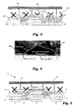
- Figure 3 schematically illustrates the formation of precipitates from said solvents
- Figure 4 shows the cross-section of a prototype formed in conformity with the prior art rules.
- the layer 46 over the wettable metal layers 18, 19a has different granulation from the portion 46' that covers the passivation layer 27.
- the underlying technical problem of this invention is to provide a method of improving the electric bonding of an electronic power device to its package such that the aforementioned two disadvantages are attenuated and/or obviated.
- the resolvent idea on which the present invention stands is one of utilizing the wettable metal line as if it were just a second metal level, and utilizing the first metal level both as a gate metal and a contact layer between the second metal level and the device source.
- the technical problem is solved by a method of fabricating an electronic power device of improved design with MOS technology, which device comprises at least one region of gate fingers and associated source regions on opposite sides of the gate region, and comprises at least one first-level metal layer, arranged to independently contact said gate region and said source regions, and a protective passivation layer over the gate region, the method being characterized in that it comprises the steps of:
- the invention further relates to a device as previously indicated and characterized in that it includes a wettable metal layer, deposited onto the passivation layer and the first-level metal layer, to extend over said source regions.
- the device 1 is fabricated on a substrate 2 of a semiconductor material to a layout known per se.
- the device 1 may be a power device fabricated with MOS technology, which has a gate middle region 3 and respective source regions 4 on opposite sides of the gate region 3.
- the device 1 is a discrete device, and has its gate region 3 formed as a so-called gate "finger", that is an elongate flat layer whose length dimension exceeds its cross dimension.
- Each region 3, 4 is contacted by a respective metal that can be regarded as a first-level metal.
- a gate metal 3' and respective source metals 4' are provided.
- a passivation layer 5 separates metal layer 3' from metal layers 4'.
- each first-level metal layer 3', 4' is a covering layer consisting of a metal layer 6, which will be wettable in the course of subsequent process steps ending in the finished electronic device.
- the wettable metal layer 6 is formed over the first-level metal layers 3' and 4', and formed laterally of the passivation layer 5, to be substantially flush with the latter.
- a soft solder 9 is provided on top of the passivation layer to also cover the wettable metal layers 6 with it.
- the structure of a conventional device is completed with a thin bridge interconnection layer 8 that extends over the solder layer 9.
- a wettable metal layer 7 advantageously extends over the passivation layer 5 in continuation of the metal layers 6 that are covering the first-level metals 4'. This layer 7 covers the passivating layer 5 completely.
- the wettable metal layer is not broken short of the gate fingers, with the benefit of eliminating a non-wettable area that gave way to the formation of precipitates in the prior art.
- first metal level one or more conductive layers that be compatible for the subsequent steps of forming the passivation layer and second metal level; they are to ensure good contact to the source and gate regions 4 and 3 of device 1.
- the passivation layer one or more insulating layers that are compatible for the step of forming the second metal level; the faultiness, integrity and dielectric rigidity of the layers should all be adequate to provide good electrical isolation of the two levels of metal from each other.
- For the second metal level one or more conductive layers effective to ensure good contact to the first metal layer and provide a solder-wettable surface for use with bridging strips in the mixed bonding method.
- the main idea is essentially in using the wettable metal as a real second metal level, and using the first level as a gate metal and contact layer between the second metal level and the source of the device.
- the two metal layers are separated by the final passivation layer.
- the wettable metal is not broken short of the gate fingers, as illustrated schematically by Figure 5.
- the region overlying the passivation layer of the gate region 3 has now been covered with a wettable metal layer. Accordingly, the area of the gate finger is utilized in this invention as a contact area of contact, with the benefit of eliminating the non-wettable area where precipitates had a chance of forming. Furthermore, the double metal levels 3', 7 provided have the advantage of ensuring a uniform distribution of the current flow even when a number of gate fingers are present, which is highly advantageous from both the rigidity and reliability standpoints.
- This first embodiment of the invention is also uniquely effective in those cases where the final bridge layer 8 is replaced with an IC chip that has to be electrical connected to one or more electrodes of the device underneath.
- This structure is known in the industry as of "chip-on-chip” and is usually obtained through the use of a conductive adhesive.
- the bridge layer 8 is shaped aligned with the gate fingers to prevent excess pressure on the device layers from causing the passivation layer 5 to crack and create undesired short-circuits across the first 3', 4' and second 7 metal levels, notably in those areas where the soft solder is laid quite thinly.
- solder layer 9 is shaped in the source regions 4, laterally of the gate fingers, to enable the bridge layer 8 to reach deeply enough to form sorts of side support legs or feet 10.
- the shaping depth is dependent on the device own inequalities (1 to 4 ⁇ m), its width being dependent on the gate finger widths and the position tolerance for the bridge layer 8 on the device 1 (50 to 300 ⁇ m).
- this technique can be applied regardless of whether the wettable metal layer 7 is provided on the gate finger.
- the shape of the bridge layer 8 may be an extended one to overlap all the area where the gate finger plurality are present. In this way, the mechanical structure of the bridge layer 8 is made simpler.
- the supporting feet 10 instead of forming supporting feet 10 on opposite sides of each gate finger, as shown in Figure 6, much broader (500 to 2000 ⁇ m) bridge layers are provided to cover a plurality of gate fingers, as shown schematically in Figure 7.
- the example of Figure 7 may be regarded as an extreme case where the layer 8 covers the whole device 1. Thanks to the supporting feet 20, the mechanical pressure is confined to within the side areas where no fingered structure occurs.
- the device and method of this invention do solve the technical problem, and afford a number of advantages by providing for the introduction of a real second metal level in discrete power devices and, where appropriate, for the bridge layer to be suitably shaped.
Landscapes
- Internal Circuitry In Semiconductor Integrated Circuit Devices (AREA)
- Junction Field-Effect Transistors (AREA)
- Coupling Device And Connection With Printed Circuit (AREA)
Abstract
Description
- The present invention broadly relates to the electric connection of an electronic power device to its package.
- In particular, but not limited to, the invention relates to a device which is fabricated with MOS technology to have at least one gate finger region and source regions on opposite sides of the gate region, the device also having at least one first-level metal layer arranged to independently contact said gate region and said source regions, and a protective passivation layer on top of the gate region.
- The invention further relates to an advantageous method of electrically bonding the power device to its package. For convenience of explanation, the description below will make reference to discrete power components.
- As is well known, factors of prime importance in electronic power devices are minimized resistive contributions (Ron) and enhanced heat dissipation from the device when in its conduction mode.
- To present, an assembly technique whereby the bonding wires are replaced with suitably shaped metal strips, or bridging strips, has met both requirements. This technique has proved itself in the instance of bipolar power devices. Also, European Patent No. 0179714 is evidence of a mixed bonding technique, whereby bonding wires are used along with bridging strips as shown in Figure 1, being known since 1985.
- Recently, an effort has been made to extend the mixed bonding technique to small packages, i.e. packages that enclose small-size integrated circuits, where contacting a pad with a clip would use up an unacceptably large amount of area. As an example, with a 7 mm2 device, contacting a gate termination by means of a clip would expend some 0.5 mm2, or 7%, of the active area. On the other hand, if a gate termination were contacted by means of a standard-gage bonding wire, the pad bulk would be brought down five times or less, i.e. to occupy less than 1% of the active area.
- For a small-size package, or micro-package, the advantages brought about by the above mixed technique are as tabulated here below:
Assembly Technique Resistive Contributions Thermal Resistance to Heat Dissipation Device-to-Package Connection Distribution of Current across Device Surface Standard 2 mΩ 1.5 mΩ 10°C/W Bridge 0.5 mΩ 0.1 mΩ 7°C/W Gain 1.5 mΩ (75%) 1.4 mΩ (93%) 3°C/W (30%) - However, this mixed bonding technique is subject to certain constraints when used with MOS devices, due to the presence of considerable fingered gate and source metal lines on the device front.
- Bonding fingered structures by means of bridges currently involves breaking the wettable metal line short of the gate fingers, e.g. as shown schematically in Figure 2.
- Figure 2 is reproduced from US Patent 6,040,626 to show a vertical cross-section taken through a gate finger. The following layers are recognizable: gate metal (19a), source metal (18), passivation (27), wettable metal (25), conductive adhesive (46), and bridge (30) layers. The lack of wettable metal in the gate finger structure results, especially in structures that are considerable fingered, in a substantial loss of contact area that reflects significantly on the device output resistance (Ron).
- In view of most of the applications on demand today favouring devices with a very low Ron and high speed for high frequency operation, avoidance of conflicting fingered structure requirements and resistive contributions is of primary concern.
- In addition, areas without wettable metal lines that extend beneath the bridge bonding are areas of doubtful adhesion into which solvents from the soft solder may flow. The structure and chemical composition of the adhesive in such areas can be quite different from that in the areas overlying the wettable metal.
- Figure 3 schematically illustrates the formation of precipitates from said solvents, and the photograph in Figure 4 shows the cross-section of a prototype formed in conformity with the prior art rules.
- In particular, the
layer 46 over thewettable metal layers passivation layer 27. - The presence of areas having different chemical compositions may damage the reliability of a product by thermal stressing, especially if fabricated in a wet environment. Thus, the above-described prior technique, related to the bridge bounding when metallization layers are not formed on the finger gate, has at least two major disadvantages:
- 1) a loss of contact area, which may grow to significance in the instance of considerable fingered devices; and
- 2) areas of uncontrolled chemical composition, which may damage reliability.
-
- The underlying technical problem of this invention is to provide a method of improving the electric bonding of an electronic power device to its package such that the aforementioned two disadvantages are attenuated and/or obviated.
- The resolvent idea on which the present invention stands is one of utilizing the wettable metal line as if it were just a second metal level, and utilizing the first metal level both as a gate metal and a contact layer between the second metal level and the device source.
- In this way, the two metal layers would be separated by a final passivation layer. In addition, breaking the wettable metal line short of the gate fingers would no longer be necessary.
- Based on this idea, the technical problem is solved by a method of fabricating an electronic power device of improved design with MOS technology, which device comprises at least one region of gate fingers and associated source regions on opposite sides of the gate region, and comprises at least one first-level metal layer, arranged to independently contact said gate region and said source regions, and a protective passivation layer over the gate region, the method being characterized in that it comprises the steps of:
- forming said first metal level over the source regions and the gate fingers;
- forming a passivation layer over the gate fingers to partly overlap the first source metal level; and
- forming a wettable metal layer, on top of the passivation layer and the first-level metal layer, to extend over said source regions.
- The invention further relates to a device as previously indicated and characterized in that it includes a wettable metal layer, deposited onto the passivation layer and the first-level metal layer, to extend over said source regions.
- The features and advantages of the method and the device according to the invention should become understood from the description of embodiments thereof, given by way of example and not of limitation with reference to the accompanying drawings.
-
- Figure 1 is a schematic perspective view of an electronic power device where a mixed bonding technique has been used for its interconnection.
- Figure 2 is a schematic enlarged-scale view in vertical cross-section of an electronic power device having a so-called interconnection gate finger.
- Figure 3 is a schematic enlarged-scale view in vertical cross-section of an electronic power device of conventional design.
- Figure 4 is a photograph of a vertical cross-section taken through the power device of Figure 3 at the gate finger thereof.
- Figure 5 is a schematic enlarged-scale view in vertical cross-section of an electronic power device formed according to the invention.
- Figure 6 is a schematic enlarged-scale view in vertical cross-section of a second embodiment of the electronic power device according to this invention.
- Figure 7 is a schematic enlarged-scale view in vertical cross-section of an electronic power device whose structure includes a plurality of gate fingers.
-
- With reference to the drawings, in particular to the embodiment shown in Figure 5, generally shown in schematic form at 1 is an electronic power device whose interconnections have been established in accordance with the inventive method.
- The
device 1 is fabricated on asubstrate 2 of a semiconductor material to a layout known per se. In other words, thedevice 1 may be a power device fabricated with MOS technology, which has agate middle region 3 andrespective source regions 4 on opposite sides of thegate region 3. - The
device 1 is a discrete device, and has itsgate region 3 formed as a so-called gate "finger", that is an elongate flat layer whose length dimension exceeds its cross dimension. - Each
region - As shown best in Figure 5, a passivation layer 5 separates metal layer 3' from metal layers 4'.
- Provided on top of each first-level metal layer 3', 4' is a covering layer consisting of a
metal layer 6, which will be wettable in the course of subsequent process steps ending in the finished electronic device. - The
wettable metal layer 6 is formed over the first-level metal layers 3' and 4', and formed laterally of the passivation layer 5, to be substantially flush with the latter. - A
soft solder 9 is provided on top of the passivation layer to also cover thewettable metal layers 6 with it. - The structure of a conventional device is completed with a thin
bridge interconnection layer 8 that extends over thesolder layer 9. - Unlike the prior art, in this invention a
wettable metal layer 7 advantageously extends over the passivation layer 5 in continuation of themetal layers 6 that are covering the first-level metals 4'. Thislayer 7 covers the passivating layer 5 completely. - In this way, the wettable metal layer is not broken short of the gate fingers, with the benefit of eliminating a non-wettable area that gave way to the formation of precipitates in the prior art.
- Summarized here below are the process steps that form the discrete type of
electronic power device 1 having at least two metal levels and a wettable final surface. As an example, the following process steps could be provided: - a first metal layer, e.g. formed by an
aluminum layer 1 to 5 µm thick, suitably doped with impurities such as silicon and/or copper impurities; - a passivation layer 0.5 to 1 µm thick of deposited oxide;
- a second, wettable metal layer, e.g. formed by a triple layer comprising a stack structure of titanium (∼1000A), nickel (∼3000A), and gold (∼500A) in a stack configuration.
-
- It should be understood that the layers mentioned above are for exemplification only, it being possible for them to be substituted with any other layers known in the semiconductor industry that exhibit the features specified here below.
- For the first metal level: one or more conductive layers that be compatible for the subsequent steps of forming the passivation layer and second metal level; they are to ensure good contact to the source and
gate regions device 1. - For the passivation layer: one or more insulating layers that are compatible for the step of forming the second metal level; the faultiness, integrity and dielectric rigidity of the layers should all be adequate to provide good electrical isolation of the two levels of metal from each other.
- For the second metal level: one or more conductive layers effective to ensure good contact to the first metal layer and provide a solder-wettable surface for use with bridging strips in the mixed bonding method.
- According to the invention, the main idea is essentially in using the wettable metal as a real second metal level, and using the first level as a gate metal and contact layer between the second metal level and the source of the device. The two metal layers are separated by the final passivation layer. In this way, the wettable metal is not broken short of the gate fingers, as illustrated schematically by Figure 5.
- From a comparison of the embodiment of Figure 5 with the prior art of Figure 3, it is evinced that the region overlying the passivation layer of the
gate region 3 has now been covered with a wettable metal layer. Accordingly, the area of the gate finger is utilized in this invention as a contact area of contact, with the benefit of eliminating the non-wettable area where precipitates had a chance of forming. Furthermore, thedouble metal levels 3', 7 provided have the advantage of ensuring a uniform distribution of the current flow even when a number of gate fingers are present, which is highly advantageous from both the rigidity and reliability standpoints. - This first embodiment of the invention is also uniquely effective in those cases where the
final bridge layer 8 is replaced with an IC chip that has to be electrical connected to one or more electrodes of the device underneath. This structure is known in the industry as of "chip-on-chip" and is usually obtained through the use of a conductive adhesive. - A second embodiment of this invention will now be described with reference to Figure 6, where co-operating parts structurally and functionally similar to those of the first embodiment shown in Figure 5 are denoted by the same reference numerals.
- In the second embodiment of this invention, the
bridge layer 8 is shaped aligned with the gate fingers to prevent excess pressure on the device layers from causing the passivation layer 5 to crack and create undesired short-circuits across the first 3', 4' and second 7 metal levels, notably in those areas where the soft solder is laid quite thinly. - Briefly, the
solder layer 9 is shaped in thesource regions 4, laterally of the gate fingers, to enable thebridge layer 8 to reach deeply enough to form sorts of side support legs orfeet 10. - The shaping depth is dependent on the device own inequalities (1 to 4 µm), its width being dependent on the gate finger widths and the position tolerance for the
bridge layer 8 on the device 1 (50 to 300 µm). - Of course, this technique can be applied regardless of whether the
wettable metal layer 7 is provided on the gate finger. - However, the greatest benefit in reliability is to be secured by combining both techniques together, because:
- the
wettable metal layer 7 on the gate fingers inhibits the formation of undesired compounds; and - the shaped
bridge layer 8 with side legs orfeet 10 resists excess pressure on the structure near the gate fingers. - For power devices that have considerable fingered areas, the shape of the
bridge layer 8 may be an extended one to overlap all the area where the gate finger plurality are present. In this way, the mechanical structure of thebridge layer 8 is made simpler. Briefly, instead of forming supportingfeet 10 on opposite sides of each gate finger, as shown in Figure 6, much broader (500 to 2000 µm) bridge layers are provided to cover a plurality of gate fingers, as shown schematically in Figure 7. The example of Figure 7 may be regarded as an extreme case where thelayer 8 covers thewhole device 1. Thanks to the supportingfeet 20, the mechanical pressure is confined to within the side areas where no fingered structure occurs. - The device and method of this invention do solve the technical problem, and afford a number of advantages by providing for the introduction of a real second metal level in discrete power devices and, where appropriate, for the bridge layer to be suitably shaped.
Claims (11)
- A method of fabricating an electronic power device (1) of improved structure with MOS technology, which device comprises at least one gate finger region (3) and corresponding source regions (3) on opposite sides of the gate region (3), at least one first-level metal layer (3',4') arranged to independently contact said gate region (3) and said source regions, and a protective passivation layer (5) covering the gate region (3), the method being characterized in that it comprises the steps of:forming said first-level metal layer (3',4') over the source regions (4) and the gate fingers (3);forming the passivation layer (5) over the gate fingers (3) in such a manner as to partly overlap the source first-level metal layer (4'); andforming a wettable metal layer (7), on top of the passivation layer (5) and the first-level metal layer placed over said source regions (4).
- A method according to Claim 1, characterized in that said wettable metal layer (7) is then covered with a solder layer (9), in turn covered with a thin bridge bonding layer (8).
- A method according to Claim 1, characterized in that said wettable metal layer (7) is a triple layer comprising a stack structure of titanium, nickel and gold.
- A method according to Claim 1, characterized in that said wettable metal layer (7) is then covered with a solder layer (9) formed with two reduced regions on opposite sides of the gate region (3); and that a thin bridge bonding layer (8) is deposited onto the solder layer (9) such that supporting feet-shaped side projections (10) from said bonding layer fit in said reduced regions.
- An electronic power device (1) of improved structure and fabricated with MOS technology to have at least one gate finger region (3) and associated source regions (4) on opposite sides of the gate region (3), the device further having at least one first-level metal layer (3',4') arranged to independently contact said gate region (3) and said source regions, and having a protective passivation layer (5) arranged to cover the gate region (3), characterized in that it includes a wettable metal layer (7) deposited onto the passivation layer (5) and the first-level metal layer (4') overlying said source regions (4).
- A device according to Claim 5, characterized in that said additional wettable metal layer (7) provides a second-level metal.
- A device according to Claim 5, characterized in that said wettable metal layer (7) is coated with a solder layer (9) covered by a thin bridge bonding layer (8).
- A device according to Claim 5, characterized in that said wettable metal layer (7) is a triple layer comprising a stack structure of titanium, nickel and gold.
- A device according to Claim 7, characterized in that said thin bridge bonding layer (8) is shaped to have supporting feet-shaped side projections (10) arranged to reach down to said source regions (4).
- A device according to Claim 7, characterized in that said thin bridge bonding layer (8) is extended to overlap the whole area occupied by the plurality of gate fingers, and has peripheral supporting projections (10) arranged to reach down to said source regions (4) on opposite sides of the gate fingers.
- A device according to Claim 5, characterized in that said wettable metal layer (7) is coated with a solder layer (9) covered by an integrated circuit chip to provide a chip-on-chip structure.
Applications Claiming Priority (2)
| Application Number | Priority Date | Filing Date | Title |
|---|---|---|---|
| IT2001MI002284A ITMI20012284A1 (en) | 2001-10-30 | 2001-10-30 | METHOD FOR IMPROVING THE ELECTRICAL CONNECTION BETWEEN AN ELECTRONIC POWER DEVICE AND ITS PACKAGE |
| ITMI20012284 | 2001-10-30 |
Publications (2)
| Publication Number | Publication Date |
|---|---|
| EP1310993A2 true EP1310993A2 (en) | 2003-05-14 |
| EP1310993A3 EP1310993A3 (en) | 2003-07-16 |
Family
ID=11448561
Family Applications (1)
| Application Number | Title | Priority Date | Filing Date |
|---|---|---|---|
| EP02024185A Ceased EP1310993A3 (en) | 2001-10-30 | 2002-10-30 | Method for enhancing the electric connection between a power electronic device and its package |
Country Status (4)
| Country | Link |
|---|---|
| US (1) | US7126173B2 (en) |
| EP (1) | EP1310993A3 (en) |
| JP (1) | JP2003152160A (en) |
| IT (1) | ITMI20012284A1 (en) |
Families Citing this family (2)
| Publication number | Priority date | Publication date | Assignee | Title |
|---|---|---|---|---|
| DE102006025959B4 (en) * | 2006-06-02 | 2010-03-04 | Infineon Technologies Ag | Power semiconductor device with front-soldered clip and method for producing such |
| US9589937B2 (en) * | 2014-08-08 | 2017-03-07 | Wuhan Xinxin Semiconductor Manufacturing Co., Ltd | Semiconductor cooling method and method of heat dissipation |
Citations (4)
| Publication number | Priority date | Publication date | Assignee | Title |
|---|---|---|---|---|
| US6055148A (en) * | 1997-07-19 | 2000-04-25 | U.S. Philips Corporation | Semiconductor device assemblies and circuits |
| US20050242393A1 (en) * | 2002-07-19 | 2005-11-03 | Renesas Technology Corp. | Semiconductor device |
| US20060022298A1 (en) * | 2004-07-30 | 2006-02-02 | Masaki Shiraishi | Semiconductor device and a manufacturing method of the same |
| US20070057350A1 (en) * | 2005-09-13 | 2007-03-15 | Ralf Otremba | Semiconductor component and method of assembling the same |
Family Cites Families (14)
| Publication number | Priority date | Publication date | Assignee | Title |
|---|---|---|---|---|
| US4067041A (en) | 1975-09-29 | 1978-01-03 | Hutson Jearld L | Semiconductor device package and method of making same |
| US4561468A (en) * | 1982-04-19 | 1985-12-31 | Valcor Engineering Corporation | Valve for use in jet engine systems and the like |
| DE3224642A1 (en) * | 1982-07-01 | 1984-01-05 | Siemens AG, 1000 Berlin und 8000 München | IGFET WITH INJECTOR ZONE |
| US4561168A (en) * | 1982-11-22 | 1985-12-31 | Siliconix Incorporated | Method of making shadow isolated metal DMOS FET device |
| EP0255970B1 (en) * | 1986-08-08 | 1993-12-15 | Philips Electronics Uk Limited | A method of manufacturing an insulated gate field effect transistor |
| US4959705A (en) * | 1988-10-17 | 1990-09-25 | Ford Microelectronics, Inc. | Three metal personalization of application specific monolithic microwave integrated circuit |
| US5404040A (en) * | 1990-12-21 | 1995-04-04 | Siliconix Incorporated | Structure and fabrication of power MOSFETs, including termination structures |
| DE69434268T2 (en) * | 1994-07-14 | 2006-01-12 | Stmicroelectronics S.R.L., Agrate Brianza | Integrated structure of a high-speed MOS technologist power device and related manufacturing method |
| US5767546A (en) | 1994-12-30 | 1998-06-16 | Siliconix Incorporated | Laternal power mosfet having metal strap layer to reduce distributed resistance |
| US5597765A (en) * | 1995-01-10 | 1997-01-28 | Siliconix Incorporated | Method for making termination structure for power MOSFET |
| US5681761A (en) * | 1995-12-28 | 1997-10-28 | Philips Electronics North America Corporation | Microwave power SOI-MOSFET with high conductivity metal gate |
| US6342715B1 (en) * | 1997-06-27 | 2002-01-29 | Kabushiki Kaisha Toshiba | Nonvolatile semiconductor memory device |
| US6040626A (en) * | 1998-09-25 | 2000-03-21 | International Rectifier Corp. | Semiconductor package |
| US6940142B2 (en) * | 2001-07-02 | 2005-09-06 | Xerox Corporation | Low data line capacitance image sensor array using air-gap metal crossover |
-
2001
- 2001-10-30 IT IT2001MI002284A patent/ITMI20012284A1/en unknown
-
2002
- 2002-10-30 US US10/285,363 patent/US7126173B2/en not_active Expired - Lifetime
- 2002-10-30 JP JP2002316673A patent/JP2003152160A/en active Pending
- 2002-10-30 EP EP02024185A patent/EP1310993A3/en not_active Ceased
Patent Citations (4)
| Publication number | Priority date | Publication date | Assignee | Title |
|---|---|---|---|---|
| US6055148A (en) * | 1997-07-19 | 2000-04-25 | U.S. Philips Corporation | Semiconductor device assemblies and circuits |
| US20050242393A1 (en) * | 2002-07-19 | 2005-11-03 | Renesas Technology Corp. | Semiconductor device |
| US20060022298A1 (en) * | 2004-07-30 | 2006-02-02 | Masaki Shiraishi | Semiconductor device and a manufacturing method of the same |
| US20070057350A1 (en) * | 2005-09-13 | 2007-03-15 | Ralf Otremba | Semiconductor component and method of assembling the same |
Non-Patent Citations (4)
| Title |
|---|
| ALLAN WARD III, ROBERT W. HENDRICKS: "Symptoms of stress-induced gain degradation in power MESFETs" * |
| I.PAWEL, R.SIEMIENIEC, M.RÖSCH: "Design of avalanche capability of power MOSFETs by device simulation" * |
| J.MOORE, H.HENDRIKS, A.MORALES: "Characterization and control of galvanic corrosion during GaAs wafer photoresist processing" * |
| K.MIZUISHI AND T. MORI: "Thermal stability of various ball-limited-metal systems under solder bumps", I-THERM '88, INTERSOCIETY CONFERENCE ON THERMAL PHENOMENA IN THE FABRICATION AND OPERATION OF ELECTRONIC COMPONENTS, 11 May 1988 (1988-05-11) - 13 May 1988 (1988-05-13), pages 67 - 70 * |
Also Published As
| Publication number | Publication date |
|---|---|
| ITMI20012284A1 (en) | 2003-04-30 |
| EP1310993A3 (en) | 2003-07-16 |
| JP2003152160A (en) | 2003-05-23 |
| US20030100154A1 (en) | 2003-05-29 |
| US7126173B2 (en) | 2006-10-24 |
Similar Documents
| Publication | Publication Date | Title |
|---|---|---|
| JP4308671B2 (en) | Semiconductor device having wire bond pad and manufacturing method thereof | |
| CN101202266B (en) | Chip-scale packaging, manufacturing method thereof, and high-power integrated circuit device | |
| US5703408A (en) | Bonding pad structure and method thereof | |
| KR100380697B1 (en) | Semiconductor Devices with Bond Pads | |
| US7494912B2 (en) | Terminal pad structures and methods of fabricating same | |
| US6696357B2 (en) | Method for manufacturing semiconductor integrated circuit devices using a conductive layer to prevent peeling between a bonding pad and an underlying insulating film | |
| JP2002164437A (en) | Power integrated circuit and method with distributed bonding and current distribution | |
| US6060378A (en) | Semiconductor bonding pad for better reliability | |
| EP3567627B1 (en) | Stress relieving structure for power semiconductor device | |
| US6649961B2 (en) | Supporting gate contacts over source region on MOSFET devices | |
| KR870000350B1 (en) | Electronic apparatus with a multiplex distributing wire system | |
| CN1074557A (en) | Semiconductor device | |
| EP0660402B1 (en) | Power semiconductor device | |
| US7126173B2 (en) | Method for enhancing the electric connection between a power electronic device and its package | |
| US10340229B2 (en) | Semiconductor device with superior crack resistivity in the metallization system | |
| CN100530577C (en) | Semiconductor device and method of manufacturing the same | |
| KR20060087516A (en) | Active area bonding compatible high current structures | |
| JPH05175191A (en) | Laminated conductive wiring | |
| US8809695B2 (en) | Contact structure for an electronic circuit substrate and electronic circuit comprising said contact structure | |
| EP2092561B1 (en) | Bond pad structure and method for producing same | |
| JP2003152160A5 (en) | ||
| US20130130445A1 (en) | Active area bonding compatible high current structures | |
| WO2003001595A2 (en) | Electronic device | |
| US20250192082A1 (en) | Semiconductor package including stacked chips | |
| CN213401191U (en) | Package structure |
Legal Events
| Date | Code | Title | Description |
|---|---|---|---|
| PUAI | Public reference made under article 153(3) epc to a published international application that has entered the european phase |
Free format text: ORIGINAL CODE: 0009012 |
|
| AK | Designated contracting states |
Designated state(s): AT BE BG CH CY CZ DE DK EE ES FI FR GB GR IE IT LI LU MC NL PT SE SK TR |
|
| AX | Request for extension of the european patent |
Extension state: AL LT LV MK RO SI |
|
| PUAL | Search report despatched |
Free format text: ORIGINAL CODE: 0009013 |
|
| AK | Designated contracting states |
Designated state(s): AT BE BG CH CY CZ DE DK EE ES FI FR GB GR IE IT LI LU MC NL PT SE SK TR |
|
| AX | Request for extension of the european patent |
Extension state: AL LT LV MK RO SI |
|
| RIC1 | Information provided on ipc code assigned before grant |
Ipc: 7H 01L 29/417 B Ipc: 7H 01L 23/485 B Ipc: 7H 01L 21/60 A |
|
| 17P | Request for examination filed |
Effective date: 20040112 |
|
| AKX | Designation fees paid |
Designated state(s): DE FR GB IT |
|
| 17Q | First examination report despatched |
Effective date: 20040621 |
|
| 17Q | First examination report despatched |
Effective date: 20040621 |
|
| RAP1 | Party data changed (applicant data changed or rights of an application transferred) |
Owner name: STMICROELECTRONICS SRL |
|
| STAA | Information on the status of an ep patent application or granted ep patent |
Free format text: STATUS: THE APPLICATION HAS BEEN REFUSED |
|
| 18R | Application refused |
Effective date: 20100224 |