EP1310949A1 - Highly orientated magnetic thin films, recording media, transducers, devices made therefrom and methods of making - Google Patents
Highly orientated magnetic thin films, recording media, transducers, devices made therefrom and methods of making Download PDFInfo
- Publication number
- EP1310949A1 EP1310949A1 EP03002468A EP03002468A EP1310949A1 EP 1310949 A1 EP1310949 A1 EP 1310949A1 EP 03002468 A EP03002468 A EP 03002468A EP 03002468 A EP03002468 A EP 03002468A EP 1310949 A1 EP1310949 A1 EP 1310949A1
- Authority
- EP
- European Patent Office
- Prior art keywords
- underlayer
- substrate
- magnetic
- recording medium
- crystal
- Prior art date
- Legal status (The legal status is an assumption and is not a legal conclusion. Google has not performed a legal analysis and makes no representation as to the accuracy of the status listed.)
- Withdrawn
Links
- 230000005291 magnetic effect Effects 0.000 title claims abstract description 294
- 239000010409 thin film Substances 0.000 title description 29
- 238000000034 method Methods 0.000 title description 22
- 239000013078 crystal Substances 0.000 claims abstract description 197
- 239000000758 substrate Substances 0.000 claims abstract description 147
- 239000000463 material Substances 0.000 claims abstract description 67
- 229910000531 Co alloy Inorganic materials 0.000 claims abstract description 54
- 238000013500 data storage Methods 0.000 claims abstract description 25
- 229910001030 Iron–nickel alloy Inorganic materials 0.000 claims description 39
- 229910045601 alloy Inorganic materials 0.000 claims description 24
- 239000000956 alloy Substances 0.000 claims description 24
- 229910021421 monocrystalline silicon Inorganic materials 0.000 claims description 19
- 239000010952 cobalt-chrome Substances 0.000 claims description 6
- 229910000684 Cobalt-chrome Inorganic materials 0.000 claims description 5
- 229910052697 platinum Inorganic materials 0.000 claims description 5
- 238000003491 array Methods 0.000 claims description 3
- 230000001419 dependent effect Effects 0.000 claims description 2
- 229910052802 copper Inorganic materials 0.000 abstract description 6
- 229910052782 aluminium Inorganic materials 0.000 abstract description 5
- 229910052737 gold Inorganic materials 0.000 abstract description 5
- 229910052751 metal Inorganic materials 0.000 abstract description 4
- 239000002184 metal Substances 0.000 abstract description 4
- 150000002739 metals Chemical class 0.000 abstract description 4
- 239000010408 film Substances 0.000 description 152
- 238000002441 X-ray diffraction Methods 0.000 description 31
- 229910019222 CoCrPt Inorganic materials 0.000 description 29
- 238000000151 deposition Methods 0.000 description 25
- 229910052804 chromium Inorganic materials 0.000 description 23
- 239000011521 glass Substances 0.000 description 23
- 229910052709 silver Inorganic materials 0.000 description 20
- 230000008021 deposition Effects 0.000 description 18
- 238000001228 spectrum Methods 0.000 description 18
- 230000001965 increasing effect Effects 0.000 description 16
- 239000000696 magnetic material Substances 0.000 description 15
- 239000000203 mixture Substances 0.000 description 13
- 230000005415 magnetization Effects 0.000 description 12
- 238000003860 storage Methods 0.000 description 12
- 229910000599 Cr alloy Inorganic materials 0.000 description 11
- 238000004544 sputter deposition Methods 0.000 description 11
- 238000009736 wetting Methods 0.000 description 11
- VYPSYNLAJGMNEJ-UHFFFAOYSA-N Silicium dioxide Chemical compound O=[Si]=O VYPSYNLAJGMNEJ-UHFFFAOYSA-N 0.000 description 10
- 235000012431 wafers Nutrition 0.000 description 8
- 238000000926 separation method Methods 0.000 description 7
- 229910052710 silicon Inorganic materials 0.000 description 7
- 239000006104 solid solution Substances 0.000 description 7
- 238000012360 testing method Methods 0.000 description 7
- 238000002524 electron diffraction data Methods 0.000 description 6
- 238000005259 measurement Methods 0.000 description 6
- 229910000889 permalloy Inorganic materials 0.000 description 6
- 230000003746 surface roughness Effects 0.000 description 6
- 229910052719 titanium Inorganic materials 0.000 description 6
- 229910015372 FeAl Inorganic materials 0.000 description 5
- 229910000943 NiAl Inorganic materials 0.000 description 5
- NPXOKRUENSOPAO-UHFFFAOYSA-N Raney nickel Chemical compound [Al].[Ni] NPXOKRUENSOPAO-UHFFFAOYSA-N 0.000 description 5
- 229910052681 coesite Inorganic materials 0.000 description 5
- 229910052906 cristobalite Inorganic materials 0.000 description 5
- 230000007423 decrease Effects 0.000 description 5
- 229910003460 diamond Inorganic materials 0.000 description 5
- 239000010432 diamond Substances 0.000 description 5
- 230000001976 improved effect Effects 0.000 description 5
- 239000000377 silicon dioxide Substances 0.000 description 5
- 229910052682 stishovite Inorganic materials 0.000 description 5
- 230000007704 transition Effects 0.000 description 5
- 229910052905 tridymite Inorganic materials 0.000 description 5
- 229910018979 CoPt Inorganic materials 0.000 description 4
- 229910017052 cobalt Inorganic materials 0.000 description 4
- 239000010941 cobalt Substances 0.000 description 4
- GUTLYIVDDKVIGB-UHFFFAOYSA-N cobalt atom Chemical compound [Co] GUTLYIVDDKVIGB-UHFFFAOYSA-N 0.000 description 4
- 238000011161 development Methods 0.000 description 4
- 239000006185 dispersion Substances 0.000 description 4
- 230000004907 flux Effects 0.000 description 4
- 230000033001 locomotion Effects 0.000 description 4
- 230000005855 radiation Effects 0.000 description 4
- FAPWRFPIFSIZLT-UHFFFAOYSA-M Sodium chloride Chemical group [Na+].[Cl-] FAPWRFPIFSIZLT-UHFFFAOYSA-M 0.000 description 3
- 230000008901 benefit Effects 0.000 description 3
- 239000000919 ceramic Substances 0.000 description 3
- 230000005347 demagnetization Effects 0.000 description 3
- 238000000407 epitaxy Methods 0.000 description 3
- 230000002349 favourable effect Effects 0.000 description 3
- 239000002241 glass-ceramic Substances 0.000 description 3
- 230000001939 inductive effect Effects 0.000 description 3
- 239000000314 lubricant Substances 0.000 description 3
- 239000012071 phase Substances 0.000 description 3
- 238000012545 processing Methods 0.000 description 3
- 229910052715 tantalum Inorganic materials 0.000 description 3
- 238000002233 thin-film X-ray diffraction Methods 0.000 description 3
- 229910052721 tungsten Inorganic materials 0.000 description 3
- 229910001149 41xx steel Inorganic materials 0.000 description 2
- OKTJSMMVPCPJKN-UHFFFAOYSA-N Carbon Chemical compound [C] OKTJSMMVPCPJKN-UHFFFAOYSA-N 0.000 description 2
- 229910003321 CoFe Inorganic materials 0.000 description 2
- 229910002441 CoNi Inorganic materials 0.000 description 2
- 229910002535 CuZn Inorganic materials 0.000 description 2
- 229910017372 Fe3Al Inorganic materials 0.000 description 2
- 229910005438 FeTi Inorganic materials 0.000 description 2
- KRHYYFGTRYWZRS-UHFFFAOYSA-N Fluorane Chemical compound F KRHYYFGTRYWZRS-UHFFFAOYSA-N 0.000 description 2
- 229910000990 Ni alloy Inorganic materials 0.000 description 2
- MCMNRKCIXSYSNV-UHFFFAOYSA-N Zirconium dioxide Chemical compound O=[Zr]=O MCMNRKCIXSYSNV-UHFFFAOYSA-N 0.000 description 2
- 230000015572 biosynthetic process Effects 0.000 description 2
- 229910052799 carbon Inorganic materials 0.000 description 2
- 230000003247 decreasing effect Effects 0.000 description 2
- 238000009826 distribution Methods 0.000 description 2
- 230000000694 effects Effects 0.000 description 2
- 230000006872 improvement Effects 0.000 description 2
- 238000011835 investigation Methods 0.000 description 2
- 238000002955 isolation Methods 0.000 description 2
- 229910052748 manganese Inorganic materials 0.000 description 2
- 230000007246 mechanism Effects 0.000 description 2
- 238000012986 modification Methods 0.000 description 2
- 230000004048 modification Effects 0.000 description 2
- 229910052750 molybdenum Inorganic materials 0.000 description 2
- 229910052759 nickel Inorganic materials 0.000 description 2
- 229910001000 nickel titanium Inorganic materials 0.000 description 2
- 230000003287 optical effect Effects 0.000 description 2
- 230000008569 process Effects 0.000 description 2
- 230000004044 response Effects 0.000 description 2
- 239000007779 soft material Substances 0.000 description 2
- 229910052726 zirconium Inorganic materials 0.000 description 2
- 229910001316 Ag alloy Inorganic materials 0.000 description 1
- 229910000838 Al alloy Inorganic materials 0.000 description 1
- 230000005330 Barkhausen effect Effects 0.000 description 1
- 229910052684 Cerium Inorganic materials 0.000 description 1
- -1 CrV Inorganic materials 0.000 description 1
- 229910002483 Cu Ka Inorganic materials 0.000 description 1
- 229910052692 Dysprosium Inorganic materials 0.000 description 1
- 229910052691 Erbium Inorganic materials 0.000 description 1
- 229910002546 FeCo Inorganic materials 0.000 description 1
- 229910015183 FeNx Inorganic materials 0.000 description 1
- 229910005347 FeSi Inorganic materials 0.000 description 1
- 229910052688 Gadolinium Inorganic materials 0.000 description 1
- 230000005374 Kerr effect Effects 0.000 description 1
- 229910000914 Mn alloy Inorganic materials 0.000 description 1
- 229910052779 Neodymium Inorganic materials 0.000 description 1
- 229920001774 Perfluoroether Polymers 0.000 description 1
- 229910052771 Terbium Inorganic materials 0.000 description 1
- 238000002083 X-ray spectrum Methods 0.000 description 1
- 238000007792 addition Methods 0.000 description 1
- 238000004458 analytical method Methods 0.000 description 1
- 238000000137 annealing Methods 0.000 description 1
- 238000013459 approach Methods 0.000 description 1
- 238000000089 atomic force micrograph Methods 0.000 description 1
- 230000009286 beneficial effect Effects 0.000 description 1
- 230000005540 biological transmission Effects 0.000 description 1
- 238000009835 boiling Methods 0.000 description 1
- 229910010293 ceramic material Inorganic materials 0.000 description 1
- 230000008859 change Effects 0.000 description 1
- KYKAJFCTULSVSH-UHFFFAOYSA-N chloro(fluoro)methane Chemical compound F[C]Cl KYKAJFCTULSVSH-UHFFFAOYSA-N 0.000 description 1
- 230000003749 cleanliness Effects 0.000 description 1
- 239000000356 contaminant Substances 0.000 description 1
- 238000011109 contamination Methods 0.000 description 1
- 238000007796 conventional method Methods 0.000 description 1
- 230000008878 coupling Effects 0.000 description 1
- 238000010168 coupling process Methods 0.000 description 1
- 238000005859 coupling reaction Methods 0.000 description 1
- 238000013480 data collection Methods 0.000 description 1
- 239000008367 deionised water Substances 0.000 description 1
- 229910021641 deionized water Inorganic materials 0.000 description 1
- 230000003111 delayed effect Effects 0.000 description 1
- 238000005137 deposition process Methods 0.000 description 1
- 238000013461 design Methods 0.000 description 1
- 238000002050 diffraction method Methods 0.000 description 1
- 238000009792 diffusion process Methods 0.000 description 1
- 239000003085 diluting agent Substances 0.000 description 1
- 238000004070 electrodeposition Methods 0.000 description 1
- 238000005566 electron beam evaporation Methods 0.000 description 1
- 230000005294 ferromagnetic effect Effects 0.000 description 1
- 239000003302 ferromagnetic material Substances 0.000 description 1
- 239000000446 fuel Substances 0.000 description 1
- 230000006870 function Effects 0.000 description 1
- 239000010931 gold Substances 0.000 description 1
- 229910002804 graphite Inorganic materials 0.000 description 1
- 239000010439 graphite Substances 0.000 description 1
- 230000003993 interaction Effects 0.000 description 1
- 238000007737 ion beam deposition Methods 0.000 description 1
- 229910052742 iron Inorganic materials 0.000 description 1
- 238000000608 laser ablation Methods 0.000 description 1
- 229910052749 magnesium Inorganic materials 0.000 description 1
- 230000005381 magnetic domain Effects 0.000 description 1
- 238000001755 magnetron sputter deposition Methods 0.000 description 1
- 238000004519 manufacturing process Methods 0.000 description 1
- 229910052758 niobium Inorganic materials 0.000 description 1
- 239000003960 organic solvent Substances 0.000 description 1
- UJMWVICAENGCRF-UHFFFAOYSA-N oxygen difluoride Chemical compound FOF UJMWVICAENGCRF-UHFFFAOYSA-N 0.000 description 1
- 230000000737 periodic effect Effects 0.000 description 1
- 230000035699 permeability Effects 0.000 description 1
- 239000000843 powder Substances 0.000 description 1
- 230000035755 proliferation Effects 0.000 description 1
- 230000001737 promoting effect Effects 0.000 description 1
- 239000000700 radioactive tracer Substances 0.000 description 1
- 238000011160 research Methods 0.000 description 1
- 239000010703 silicon Substances 0.000 description 1
- 239000011780 sodium chloride Substances 0.000 description 1
- 239000007787 solid Substances 0.000 description 1
- 239000000126 substance Substances 0.000 description 1
- 239000000725 suspension Substances 0.000 description 1
- 238000002207 thermal evaporation Methods 0.000 description 1
- 229910052723 transition metal Inorganic materials 0.000 description 1
- 229910052720 vanadium Inorganic materials 0.000 description 1
- LEONUFNNVUYDNQ-UHFFFAOYSA-N vanadium atom Chemical compound [V] LEONUFNNVUYDNQ-UHFFFAOYSA-N 0.000 description 1
- 238000001947 vapour-phase growth Methods 0.000 description 1
- 230000035899 viability Effects 0.000 description 1
- XLYOFNOQVPJJNP-UHFFFAOYSA-N water Chemical compound O XLYOFNOQVPJJNP-UHFFFAOYSA-N 0.000 description 1
- 229910052727 yttrium Inorganic materials 0.000 description 1
Images


Classifications
-
- G—PHYSICS
- G11—INFORMATION STORAGE
- G11B—INFORMATION STORAGE BASED ON RELATIVE MOVEMENT BETWEEN RECORD CARRIER AND TRANSDUCER
- G11B5/00—Recording by magnetisation or demagnetisation of a record carrier; Reproducing by magnetic means; Record carriers therefor
- G11B5/62—Record carriers characterised by the selection of the material
- G11B5/64—Record carriers characterised by the selection of the material comprising only the magnetic material without bonding agent
- G11B5/66—Record carriers characterised by the selection of the material comprising only the magnetic material without bonding agent the record carriers consisting of several layers
- G11B5/676—Record carriers characterised by the selection of the material comprising only the magnetic material without bonding agent the record carriers consisting of several layers having magnetic layers separated by a nonmagnetic layer, e.g. antiferromagnetic layer, Cu layer or coupling layer
-
- G—PHYSICS
- G11—INFORMATION STORAGE
- G11B—INFORMATION STORAGE BASED ON RELATIVE MOVEMENT BETWEEN RECORD CARRIER AND TRANSDUCER
- G11B5/00—Recording by magnetisation or demagnetisation of a record carrier; Reproducing by magnetic means; Record carriers therefor
- G11B5/127—Structure or manufacture of heads, e.g. inductive
- G11B5/1278—Structure or manufacture of heads, e.g. inductive specially adapted for magnetisations perpendicular to the surface of the record carrier
-
- G—PHYSICS
- G11—INFORMATION STORAGE
- G11B—INFORMATION STORAGE BASED ON RELATIVE MOVEMENT BETWEEN RECORD CARRIER AND TRANSDUCER
- G11B5/00—Recording by magnetisation or demagnetisation of a record carrier; Reproducing by magnetic means; Record carriers therefor
- G11B5/62—Record carriers characterised by the selection of the material
- G11B5/73—Base layers, i.e. all non-magnetic layers lying under a lowermost magnetic recording layer, e.g. including any non-magnetic layer in between a first magnetic recording layer and either an underlying substrate or a soft magnetic underlayer
- G11B5/736—Non-magnetic layer under a soft magnetic layer, e.g. between a substrate and a soft magnetic underlayer [SUL] or a keeper layer
-
- G—PHYSICS
- G11—INFORMATION STORAGE
- G11B—INFORMATION STORAGE BASED ON RELATIVE MOVEMENT BETWEEN RECORD CARRIER AND TRANSDUCER
- G11B5/00—Recording by magnetisation or demagnetisation of a record carrier; Reproducing by magnetic means; Record carriers therefor
- G11B5/62—Record carriers characterised by the selection of the material
- G11B5/73—Base layers, i.e. all non-magnetic layers lying under a lowermost magnetic recording layer, e.g. including any non-magnetic layer in between a first magnetic recording layer and either an underlying substrate or a soft magnetic underlayer
- G11B5/7368—Non-polymeric layer under the lowermost magnetic recording layer
- G11B5/7369—Two or more non-magnetic underlayers, e.g. seed layers or barrier layers
- G11B5/737—Physical structure of underlayer, e.g. texture
-
- G—PHYSICS
- G11—INFORMATION STORAGE
- G11B—INFORMATION STORAGE BASED ON RELATIVE MOVEMENT BETWEEN RECORD CARRIER AND TRANSDUCER
- G11B5/00—Recording by magnetisation or demagnetisation of a record carrier; Reproducing by magnetic means; Record carriers therefor
- G11B5/62—Record carriers characterised by the selection of the material
- G11B5/73—Base layers, i.e. all non-magnetic layers lying under a lowermost magnetic recording layer, e.g. including any non-magnetic layer in between a first magnetic recording layer and either an underlying substrate or a soft magnetic underlayer
- G11B5/739—Magnetic recording media substrates
- G11B5/73911—Inorganic substrates
- G11B5/73913—Composites or coated substrates
-
- G—PHYSICS
- G11—INFORMATION STORAGE
- G11B—INFORMATION STORAGE BASED ON RELATIVE MOVEMENT BETWEEN RECORD CARRIER AND TRANSDUCER
- G11B5/00—Recording by magnetisation or demagnetisation of a record carrier; Reproducing by magnetic means; Record carriers therefor
- G11B5/62—Record carriers characterised by the selection of the material
- G11B5/73—Base layers, i.e. all non-magnetic layers lying under a lowermost magnetic recording layer, e.g. including any non-magnetic layer in between a first magnetic recording layer and either an underlying substrate or a soft magnetic underlayer
- G11B5/739—Magnetic recording media substrates
- G11B5/73911—Inorganic substrates
- G11B5/73917—Metallic substrates, i.e. elemental metal or metal alloy substrates
- G11B5/73919—Aluminium or titanium elemental or alloy substrates
-
- G—PHYSICS
- G11—INFORMATION STORAGE
- G11B—INFORMATION STORAGE BASED ON RELATIVE MOVEMENT BETWEEN RECORD CARRIER AND TRANSDUCER
- G11B5/00—Recording by magnetisation or demagnetisation of a record carrier; Reproducing by magnetic means; Record carriers therefor
- G11B5/62—Record carriers characterised by the selection of the material
- G11B5/73—Base layers, i.e. all non-magnetic layers lying under a lowermost magnetic recording layer, e.g. including any non-magnetic layer in between a first magnetic recording layer and either an underlying substrate or a soft magnetic underlayer
- G11B5/739—Magnetic recording media substrates
- G11B5/73911—Inorganic substrates
- G11B5/73921—Glass or ceramic substrates
-
- H—ELECTRICITY
- H01—ELECTRIC ELEMENTS
- H01F—MAGNETS; INDUCTANCES; TRANSFORMERS; SELECTION OF MATERIALS FOR THEIR MAGNETIC PROPERTIES
- H01F10/00—Thin magnetic films, e.g. of one-domain structure
- H01F10/08—Thin magnetic films, e.g. of one-domain structure characterised by magnetic layers
- H01F10/10—Thin magnetic films, e.g. of one-domain structure characterised by magnetic layers characterised by the composition
- H01F10/12—Thin magnetic films, e.g. of one-domain structure characterised by magnetic layers characterised by the composition being metals or alloys
- H01F10/16—Thin magnetic films, e.g. of one-domain structure characterised by magnetic layers characterised by the composition being metals or alloys containing cobalt
-
- G—PHYSICS
- G11—INFORMATION STORAGE
- G11B—INFORMATION STORAGE BASED ON RELATIVE MOVEMENT BETWEEN RECORD CARRIER AND TRANSDUCER
- G11B5/00—Recording by magnetisation or demagnetisation of a record carrier; Reproducing by magnetic means; Record carriers therefor
- G11B2005/0002—Special dispositions or recording techniques
- G11B2005/0026—Pulse recording
- G11B2005/0029—Pulse recording using magnetisation components of the recording layer disposed mainly perpendicularly to the record carrier surface
-
- G—PHYSICS
- G11—INFORMATION STORAGE
- G11B—INFORMATION STORAGE BASED ON RELATIVE MOVEMENT BETWEEN RECORD CARRIER AND TRANSDUCER
- G11B2220/00—Record carriers by type
- G11B2220/20—Disc-shaped record carriers
- G11B2220/25—Disc-shaped record carriers characterised in that the disc is based on a specific recording technology
- G11B2220/2508—Magnetic discs
-
- G—PHYSICS
- G11—INFORMATION STORAGE
- G11B—INFORMATION STORAGE BASED ON RELATIVE MOVEMENT BETWEEN RECORD CARRIER AND TRANSDUCER
- G11B2220/00—Record carriers by type
- G11B2220/20—Disc-shaped record carriers
- G11B2220/25—Disc-shaped record carriers characterised in that the disc is based on a specific recording technology
- G11B2220/2525—Magneto-optical [MO] discs
-
- Y—GENERAL TAGGING OF NEW TECHNOLOGICAL DEVELOPMENTS; GENERAL TAGGING OF CROSS-SECTIONAL TECHNOLOGIES SPANNING OVER SEVERAL SECTIONS OF THE IPC; TECHNICAL SUBJECTS COVERED BY FORMER USPC CROSS-REFERENCE ART COLLECTIONS [XRACs] AND DIGESTS
- Y10—TECHNICAL SUBJECTS COVERED BY FORMER USPC
- Y10S—TECHNICAL SUBJECTS COVERED BY FORMER USPC CROSS-REFERENCE ART COLLECTIONS [XRACs] AND DIGESTS
- Y10S428/00—Stock material or miscellaneous articles
- Y10S428/90—Magnetic feature
-
- Y—GENERAL TAGGING OF NEW TECHNOLOGICAL DEVELOPMENTS; GENERAL TAGGING OF CROSS-SECTIONAL TECHNOLOGIES SPANNING OVER SEVERAL SECTIONS OF THE IPC; TECHNICAL SUBJECTS COVERED BY FORMER USPC CROSS-REFERENCE ART COLLECTIONS [XRACs] AND DIGESTS
- Y10—TECHNICAL SUBJECTS COVERED BY FORMER USPC
- Y10T—TECHNICAL SUBJECTS COVERED BY FORMER US CLASSIFICATION
- Y10T428/00—Stock material or miscellaneous articles
- Y10T428/12—All metal or with adjacent metals
- Y10T428/12493—Composite; i.e., plural, adjacent, spatially distinct metal components [e.g., layers, joint, etc.]
- Y10T428/12535—Composite; i.e., plural, adjacent, spatially distinct metal components [e.g., layers, joint, etc.] with additional, spatially distinct nonmetal component
- Y10T428/12611—Oxide-containing component
-
- Y—GENERAL TAGGING OF NEW TECHNOLOGICAL DEVELOPMENTS; GENERAL TAGGING OF CROSS-SECTIONAL TECHNOLOGIES SPANNING OVER SEVERAL SECTIONS OF THE IPC; TECHNICAL SUBJECTS COVERED BY FORMER USPC CROSS-REFERENCE ART COLLECTIONS [XRACs] AND DIGESTS
- Y10—TECHNICAL SUBJECTS COVERED BY FORMER USPC
- Y10T—TECHNICAL SUBJECTS COVERED BY FORMER US CLASSIFICATION
- Y10T428/00—Stock material or miscellaneous articles
- Y10T428/26—Web or sheet containing structurally defined element or component, the element or component having a specified physical dimension
- Y10T428/263—Coating layer not in excess of 5 mils thick or equivalent
- Y10T428/264—Up to 3 mils
- Y10T428/265—1 mil or less
Definitions
- the present invention is directed generally to thin films, magnetic recording media, transducers and devices incorporating the films and, more particularly, to thin films promoting highly oriented cobalt or cobalt alloy magnetic layers for use in magnetic recording media and transducers.
- Computational and data manipulation devices are being used in a rapidly expanding number of applications. Examples of these include supercomputers, personal desk top and portable laptop computers, file servers, personal data assistants, data collection devices, article tracking systems, video recorders, digital audio recorders, and even telephone answering machines.
- a common architectural feature is that they all have a central processing unit, input-output interfaces, various levels of temporary memory, and usually some form of permanent data storage device.
- the distinguishing characteristic of the permanent data storage device is that the information remains intact even if the electrical power is lost or removed.
- Data are stored on permanent data storage devices either optically or magnetically. The more commonly used data storage devices are based upon magnetic materials which are erasable and re-recordable. Common to all magnetic data storage devices are record and read transducers, a magnetic medium upon which to store the data, and a mechanism to position the medium or the transducers relative to one another.
- Some of the more common permanent data storage devices include the floppy disk drive, the hard disk drive, and the magneto-optic disk drive in which data are stored in magnetic bits in segmented circular tracks.
- the magnetic medium is rotated and the transducers are stationary or moved radially to read or write data at a location on the medium.
- the magnetic medium is sometimes constructed as a tape or a sheet and is transported linearly while the transducers may be stationary, moved transversely across the moving medium, or even moved in a helical arc relative to the medium.
- very large amounts of data may be stored on physically very small formats where the medium or the transducers are moved in two dimensional Cartesian coordinates or arc motions relative to each other to access the data.
- the transducers for many of the non-optical magnetic data storage systems have been inductive magnetic heads used for recording data by magnetizing the medium in a particular direction and for reading the data by detecting the direction of the magnetized medium. More recently, an inductive magnetic head is used for recording the data pattern while a magnetoresistive sensor is used for reading the data.
- an integral part of the record transducer is a component which generates a magnetic field at the medium surface while the surface is heated by using an optical source. The medium magnetization then assumes the magnetic orientation of the field generated by the record transducer when the medium cools. In some systems this orienting field is provided by an adjancent magnetic material.
- the magnetic medium Due to the physical size, efficiency and orientation of the record and read transducers the magnetic medium is generally magnetized in a preferred orientation. Hence, in almost all magnetic data storage media it is desired to orient the magnetic media in a direction to match the operational orientation of the recording and playback transducer. In addition, magnetic materials generally will magnetize more easily in a preferred orientation or orientations, along what are known as a magnetically easy axis or axes.
- Magnetic properties such as coercivity (H c ), remanant magnetization (M r ) and coercive squareness (S*), are crucial to the recording performance of the medium. These magnetic properties are primarily, dependent on the microstructure of the film for a fixed composition.
- the magnetized layer preferably has uniaxial crystalline anisotropy and a magnetization easy axis directed along the c-axis and predominately in the plane of the film (i.e, in-plane).
- the predominate crystallographic orientation of a layer is known as the crystallographic texture, or texture, as used herein, as opposed to the use of the term "texture" to describe the mechanical roughness of a surface.
- a crystal having a surface and a crystallographic plane parallel to the surface would be said to have a texture described by a direction vector orthogonal to the surface.
- the better the in-plane c-axis orientation the higher the coercivity of the magnetic layer used for longitudinal recording. High coercivity is required to achieve a high remanence.
- the desired crystalline structure of the Co alloys is hexagonal close packed ("hcp") with the uniaxial anisotropy and crystalline c-axis perpendicular to the film plane.
- the orientation of the medium be either random parallel to or constant in relation to the circumferential direction in the plane of the medium or that the orientation be perpendicular to the medium surface.
- the relative orientations of the magnetic medium and the transducers does not vary as the medium is rotated relative to the transducers. Variations in the relative orientations of the medium and the transducers results in variations in the recording and reading of signals, which is known as signal modulation.
- the orientation is nearly random in the plane of the medium.
- rotating magnetic media often have some small degree of orientation along the record track direction due to the mechanical roughness of the substrate surface.
- the orientation must be well oriented perpendicular to the media plane to match the field orientation of the record and read transducers.
- the magneto-optical Faraday effect, or Kerr effect is far larger when the light propagates parallel to the magnetization direction. Because the light is usually delivered perpendicular to the medium surface, it is desired that the magnetic orientation of the medium be the same.
- the preferred magnetic orientation of the media is parallel to the field orientation of the transducers.
- Modern high performance magnetic media generally consist of one or more thin magnetic films supported on a substrate.
- the thin films are generally vacuum deposited on the substrate by various techniques such as thermal or electron beam evaporation, RF or DC diode or magnetron sputtering, ion beam deposition, laser ablation, or chemical vapor phase deposition.
- films have also been prepared by electrochemical deposition.
- the thin film layers are polycrystalline.
- the magnetic thin film layers are composed of amorphous rare earth-transition metal alloys, but polycrystalline superlattices have also been used.
- the substrate can be made from a glass, a glass ceramic, or ceramic, but is more commonly an AlMg alloy with a NiP layer which is electrolessly plated on the surface.
- the size and separation of the individual grains not only affects the media noise and recording density achievable on the layer, but the separation also affects the achievable separation of the recorded data transitions, or signal, the degree of overlap of which induces additional media noise in the signal.
- Cobalt-based alloys as opposed to pure cobalt are commonly used in longitudinal and perpendicular magnetic media for a variety of reasons.
- non-magnetic elements such as Cr are commonly bulk doped into the magnetic film to lower the magnetization. This is especially important in perpendicular media where the demagnetization energy associated with the magnetic moment of the alloy must be less than the magneto-crystalline anisotropy energy in order for the magnetization to be oriented perpendicular to the media film plane.
- the same technique is used in longitudinal magnetic media to lower the flux transition demagnetization energy, resulting in a shorter flux transition length and, hence, higher recording densities.
- non-magnetic elements are introduced into the Co-alloy to provide grain to grain isolation via non-ferromagnetic material diffusion to limit the magnetic exchange coupling between cobalt grains.
- the Co alloy thin film should have uniformly sized, small grains with grain boundaries which can magnetically isolate neighboring grains. This kind of microstructure, orientation, and crystallographic texture is normally achieved by manipulating the deposition process, by grooving the substrate surface, by varying the cobalt alloy composition or by the proper use of underlayers.
- the grain size and orientation quality of the magnetic thin film layers are largely determined by the grain size and texture quality of the layer upon which the layer is being-deposited.
- the degree to which a prior layer can be made to induce a texture in a second layer depends, in part, upon the relative size, or lattice spacing and the crystal structure, of the material in each layer.
- the crystallographic texture will not be replicated and the layer will be deposited with either an amorphous structure and/or in an orientation of the crystal structure independent of the underlayer and representative of the lowest energy state, i.e. closest packed structure, depending upon the material.
- the underlayer alloy composition can be chosen to vary the atomic crystalline lattice parameter to better match the lattice spacing of the Co alloy.
- the hcp Co alloys have a high uniaxial anisotropy constant, along the hcp c-axis, which is necessary to achieve a high coercivity in the magnetic media.
- the Co alloy is epitaxially grown upon a random in the plane orientation of bcc Cr crystallites to prevent signal modulation. That is, the Co should be oriented with a preferred set of crystal planes parallel to the substrate surface plane.
- Cr textures are suitable to grow Co with its magnetic easy axis in or near the film plane. For example, K. Hono, B. Wong, and D.E. Laughlin, "Crystallography of Co/Cr bilayer magnetic thin films", Journal of Applied Physics 68 (9) p.
- textured Cr grain 2 possible c-axis orientations can grow (bi-crystal) while upon a single (110) textured Cr grain 4 possible c-axis orientations of Cr can grow (quad-crystal). If these variants do coexist on single Cr alloy grains, the bi-crystals and quad-crystals then can never have all of the c-axes simultaneously parallel to the applied field and the coercivities of the grains will be decreased.
- the very uncommon uni-crystal Co(10 1 0)//Cr(112) texture relationship only allows a single orientation upon a Cr grain and results in a higher coercivity whether the Cr grains are randomly oriented in the film plane or oriented parallel to the recording field direction.
- the desirable Cr (112) texture which is required to obtain the uni-crystal, is not often seen except when Cr is made unsuitably thick for media and at which point the Cr crystallites are growing in all directions and the film is usually showing multiple textures similar to a polycrystalline powder.
- the magnetic layer structure includes multiple seed layers, multiple underlayers, and intermediate layers.
- seed layers can be incorporated between the underlayer and the substrate to provide additional control of the structure of the underlayer, control the roughness of the films, and to prevent contamination of the underlayer by the substrate contaminants.
- the multiple seed layers, multiple underlayers, and intermediate layers are collectively referred to herein as the underlayer structure.
- multiple magnetic layers that may or may not be separated by a non-ferromagnetic inner layer such as Cr or Cr alloys are sometimes employed to produce variations in the magnetic properties of the resulting film.
- the magnetic layers and intervening inner layers are collectively referred to herein as the magnetic layer structure.
- multi-layered underlayer and magnetic layer structures can provide for increased control over the grain size, the grain to grain isolation and epitaxial growth of subsequent layers and the surface roughness of the magnetic layers.
- additional layers will also increase the overall cost and complexity of the manufacturing process.
- the Co alloy c-axis be perpendicular to the substrate plane.
- the Co alloy has a (0002) texture and the [0002] crystal direction is perpendicular to the film plane. It has been found that if Co is grown fairly thick that this texture naturally develops as the (0002) plane of atoms are closest packed. However, this is unsuitable for media as a large dispersion in this orientation results and the first portion of these films have random or extremely poor orientation.
- the degree of orientation must be exceptionally good for perpendicular recording as the perpendicular head field patterns have low field gradients because there is no return path for the field flux. To date there has been no commercially viable products using perpendicular thin film recording media that are comparable in terms of longitudinal thin film recording products.
- Magnetic recording and playback transducers are composed of soft magnetic materials such as CoZr, FeN x , FeAlN x , FeTaN x , FeSi alloys, NiFe alloys or FeCo alloys. Analogous to the media in order to produce high performance transducers it is necessary to control the crystallographic orientation, magnetic anisotropy magnitude and orientation, and grain size, as well as, magnetostrictive and magnetoelastic properties, and localized stresses in the material. Without control of these attributes and factors the transducer may have undesirably large hysteretic properties, remain magnetized even after the drive signal has been removed, exhibit Barkhausen phenomena or time delayed noise spikes, or exhibit non-linear response to field signals.
- soft magnetic materials such as CoZr, FeN x , FeAlN x , FeTaN x , FeSi alloys, NiFe alloys or FeCo alloys.
- vacuum deposited seed layers are sometimes employed to induce the fcc Ni alloy to have a (111) texture.
- the easy magnetic axes lie along the ⁇ 111> directions so if a (111) texture is induced the easy axes to lie only 19° from the film plane. The quality of this orientation plays a significant role in determining the uniformity of the magnetic spin rotation or the magnetic domain wall motion in these layers.
- magnetoresistive or spin valve sensors it is common to use hard magnetic materials, very similar to those used in magnetic recording media, to provide magnetic biasing to the soft magnetic materials.
- hard magnetic materials very similar to those used in magnetic recording media
- CoPt for this purpose.
- texture quality in order to improve the anisotropy and the coercivity of these device elements.
- materials and thin film device structures which will yield a high degree of orientation and uniformity of the magnetic film properties.
- the present invention is directed to thin films, magnetic and magneto-optic recording media, transducers and devices incorporating the films.
- the thin film material structures generally include a substrate, an underlayer structure which includes an underlayer and may include one or more additional underlayers, seed and/or wetting layers, and intermediate layers, and a magnetic layer structure, which includes a magnetic layer and may include one or more additional magnetic layers and inner nonmagnetic layers disposed between the magnetic layers.
- the recording medium includes a magnetic recording layer comprised of Co-based material, such as Co or one or more Co alloys having a (10 1 0) crystal texture, a substrate, a first underlayer having a fcc structure and a (110) crystal texture disposed between the substrate and the magnetic recording layer.
- a second underlayer having a bcc structure and a (112) crystal texture is also disposed between the magnetic recording layer and the first underlayer.
- the first and second underlayers are comprised of Ag and Cr, respectively, and the substrate is a single crystal Si substrate having a (110) orientation.
- a conventional substrate having a polycrystalline fcc structure seed layer or underlayer, deposited on the substrate with a (110) crystal texture can be used.
- Bcc structure such as Cr, or a bcc derivative, such as NiAl, FeAl (B2), or Fe 3 Al, AlNi 2 Ta, AlNi 2 Nb (DO3), AlNi 2 Ti (DO3 +B2) or L2 1 structures can be epitaxially grown upon the fcc structure.
- a bcc derivative such as NiAl, FeAl (B2), or Fe 3 Al, AlNi 2 Ta, AlNi 2 Nb (DO3), AlNi 2 Ti (DO3 +B2) or L2 1 structures can be epitaxially grown upon the fcc structure.
- the recording medium includes a magnetic recording layer comprised of Co-based material, such as Co or one or more Co alloys having a (11 2 0) crystal texture, a substrate, a first underlayer having a fcc structure and a (001) crystal texture disposed between the substrate and the magnetic recording layer.
- a second underlayer having a bcc structure and a (001) crystal texture is also disposed between the magnetic recording layer and the first underlayer.
- the first and second underlayers are comprised of Ag and Cr, respectively
- the substrate is a single crystal Si substrate having a (001) crystal texture or a conventional substrate having a polycrystalline seed layer, such as MgO, having a (001) crystal texture.
- the recording media includes a magnetic recording layer comprised of Co-based material, such as Co or one or more Co alloys having a (10 1 1) crystal texture, a substrate, a first underlayer having a fcc structure and a (111) crystal texture disposed between the substrate and the magnetic recording layer.
- a second underlayer having a bcc structure and a (110) crystal texture is also disposed between the magnetic recording layer and the first underlayer.
- the first and second underlayers are comprised of Ag and Cr, respectively, and the substrate is a single crystal Si substrate having a (111) orientation or a conventional substrate having a polycrystalline bcc structure seed layer or underlayer, deposited on the substrate with a (110) crystal texture.
- perpendicular recording media and transducers include a hard magnetic layer, such as a Co-based material, having a (0002) crystal texture deposited on hcp (0002) template, such as Ti, or a compatibly matched fcc (111) structure, such as Cu, which may be further deposited on a Ag (111) layer.
- a Si (111) substrate can used to provide the template for the growth of the fcc (111) structure or a conventional substrate having a polycrystalline bcc structure seed layer or underlayer, deposited on the substrate with a (110) crystal texture.
- the perpendicular media and transducers can be constructed using soft magnetic material, such as NiFe alloys, deposited with a (111) on one or more fcc (111) structures, preferably Cu (111) on Ag (111).
- soft magnetic material such as NiFe alloys
- a (111) on one or more fcc (111) structures preferably Cu (111) on Ag (111).
- the oriented soft magnetic layer can be incorporated into transducers and recording media in the presence or absence of hard magnetic layers depending upon the particular application.
- the present invention provides for highly oriented magnetic recording media, transducers and data storage devices incorporating recording media and transducers having high coercivity and lower noise and cost for use in hard disk drives and other applications.
- the material structures of the invention can be embodied in recording media and transducers used to record and read data on the recording media.
- the recording media can be used in rotating, translating, or stationary data storage devices, such as a rigid magnetic hard disc incorporated into a disc drive of a computer(not shown).
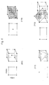
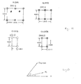
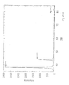
- data storage devices 8 include a recording medium 10 and a transducer 11 in a head, or slider, that is either stationary or supported on a movable arm in a suspension assembly used for moving the head over the surface of the medium 10, as shown in Fig. 1.
- the transducer 11 is maintained in a closely spaced, parallel relationship relative to the surface of the medium 10 during normal operation.
- a typical distance between the head and the medium is 10 ⁇ in or less. See, Mee, C.D. and Daniel, E.D., MAGNETIC RECORDING, Vols. I - III (McGraw-Hill pub. 1987); F. Jorgenson, The Complete Handbook of Magnetic Recording, Chapter 16 (3rd. ed. 1988), and U.S. Patent No. 5,062,021, the relevant disclosures of which are incorporated herein by reference.
- the material structure of the recording medium 10 and transducer 11 will have the nomenclature described below.
- the material structure in the recording medium 10 and transducer 11 of the present invention is comprised of a substrate 12, an underlayer 14, and a magnetic layer 16.
- the material structure might include a plurality of underlayers and/or magnetic layers that define an underlayer structure and magnetic layer structure, respectively.
- the underlayer structure may also include a seed layer and/or a wetting layer 18 disposed on the substrate 12 or elsewhere within,the underlayer structure, additional underlayers 20 'and an intermediate layer 22 disposed on the underlayer 14 adjacent to the magnetic layer structure.
- the magnetic layer 16 may be covered with an overlayer structure including an overlayer 24 followed by an overcoat 26 and an organic lubricant 28.
- the wetting layer 18 can be an amorphous material or a film too thin to have developed a crystalline structure, or a film whose texture provides a gross lattice mismatch for the ensuing layer.
- the magnetic layer structure may include additional magnetic layers, 16' and 16", that may be separated by one or more inner layers 30.
- the additional magnetic layers 16' and 16" may be soft magnetic keeper layers surrounding the magnetic layer 16 which may a magnetically hard material.
- the magnetic layer 16 in Fig. 2(a) may be a magnetically hard or soft material depending on the function of the layer in the transducer 11 being used to read or record data on the medium 10.
- the substrate 12 is formed of a nonmagnetic material, such as glass, silicon or an aluminum alloy coated with NiP, glass ceramic, ceramic, or SiC.
- a nonmagnetic material such as glass, silicon or an aluminum alloy coated with NiP, glass ceramic, ceramic, or SiC.
- the magnetic layers, 16, 16', and 16'' are deposited with the longitudinal magnetic easy axis thereof substantially parallel to the plane of such magnetic layer.
- the magnetically hard materials used in the magnetic layers 16 of the present invention are preferably a Co or Co alloy film, such as CoCr, CoSm, CoPr, CoP, CoNi, CoPt, CoNiCr, CoNiZr, CoPtNi, CoCrTa, CoCrPt, CoCrP, CoCrTaSi, CoCrPtSi, CoCrPtB, CoCrPtTa, CoCrPtTaB, CoCrPtTaNb or other known Co alloy magnetic films.
- the magnetic layers 16 are each about 2.5 - 60 nm (25 - 600 ⁇ ) thick.
- the magnetic layers 16 may also include soft magnetic materials, such NiFe alloys, particularly in perpendicular recording applications as further discussed within.
- the wetting and/or seed layer 18 can be disposed between various layers in the medium 10 to either destroy the texture of the prior film or to provide a different texture upon which subsequent layer will be epitaxially grown depending upon whether a wetting or seed layer is used, respectively.
- the underlayers 14 and 20 are generally comprised of a material suitable for producing epitaxial growth of the magnetic layer 16 as will be discussed further below.
- the overlayer 24 may be provided adjacent to and preferably in contact with the magnetic layer 16 or 16".
- the overlayer 24 is preferably 1 - 10 nm (10-100 ⁇ ) thick and may be made of W, Ta, Zr, Ti, Y, Pt, Cr, Mn, Mn alloy or any combination thereof.
- the overcoat 26 may be provided external to the overlayer 24, so that the overlayer 24 is positioned between the magnetic layer 16 or 16" and the overcoat 24, as shown in Figs. 1(b) and (c).
- the overcoat 26 provides a mechanical wear layer and is 2.5 - 30 nm (25-300 ⁇ ) thick. It is preferably made of a ceramic material or diamond-like carbon, such as SiO 2 , SiC, CH x or CN x (where x ⁇ 1), ZrO 2 , or C.
- the organic lubricant 28 may be disposed on the overcoat 26.
- the lubricant 28 is 1 nm to 10 nm (10 to 100 ⁇ ) thick and is preferably a fluoro-chlorocarbon or a perfluoroether.
- Examples include CCl 2 FCClF 2 , CF 3 (CF 2 ) 4 CF 3 , CF 3 (CF 2 ) 5 CF 3 , CF 3 (CF 2 ) 10 CF 3 , and CF 3 (CF 2 ) 16 CF 3 .
- Co-based alloy polycrystalline thin film magnetic layers having a random magnetic orientation in the film plane formed on Cr-based underlayers are currently the ' most popular structures for thin-film longitudinal recording media. These structures have a sufficiently high coercivity to meet the current industry recording density demands.
- An important parameter for assessing the achievable coercivity of a material is the anisotropy field constant H K , which is defined as 2 K 1 / M s , where K 1 is the uniaxial anisotropy constant and M s is the saturation magnetization, both of which are intrinsic material properties.
- H c the highest coercivity that can conceptually be realized, as determined by the Stoner-Wohlfarth model of rotation magnetization, is 0.51 H K .
- the single domain grains are randomly oriented in 3 dimensions the maximum achievable coercivity is considerably less than 0.51 H K .
- Current industry efforts are being devoted to trying to approach this ideal H c for two dimensional random polycrystalline Co films.
- a compatible atomic lattice structure represents structures having atomic spacings along the various crystalline directions that are comparable or differ by integer multiples to allow either one to one unit cell alignment or alignment over a repeatable mesh of unit cells.
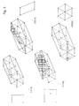
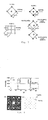
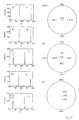
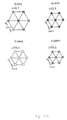
- the face centered cubic structure shown in Fig. 4 encompasses pure elements having a fcc structure, as well as solid solutions of those pure elements and alloys having derivative structures, such as L1 0 and L1 2 , that have a unit cell analogous to the fcc unit cell.
- the use of the terms "fcc” and “fcc structure” herein should be understood to include those compositions that have a face centered cubic structure or face centered cubic derivative structure, unless otherwise stated.
- Other compositions have different unit cell structures that are based on the fcc Bravais lattice, such as diamond (Fig. 5) and NaCl. While these compositions are not fcc structures, the compositions are said to have a Bravais lattice that is fcc and reference to these structures will be made in terms of the fcc Bravais lattice compositions.
- fcc structured underlayer In the present invention, Ag or an Ag alloy is generally preferred as the fcc structured underlayer, but other suitable material having a fcc structure include Ag, Cu, Al, Au and solid solution and alloy combinations thereof.
- suitable material having a fcc structure include Ag, Cu, Al, Au and solid solution and alloy combinations thereof.
- the precise choice of the fcc structure underlayer material depends upon the desired composition and orientation of the magnetic layer as will become further evident within.
- the first underlayer which has a face centered cubic crystal structure and a (001) orientation
- the first underlayer can be used to induce epitaxial growth of a second underlayer a body centered cubic structure (Fig. 6) and a (001) crystal texture and a compatible atomic spacing, which, in turn, can induce the growth of a material having a hcp structure in a (11 2 0) crystal orientation.
- body centered cubic structure shown in Fig. 6 encompasses pure elements having a bcc structure, as well as solid solutions of those pure elements and alloys having derivative structures, such as B2, DO3 and L2 1 , that have a unit cell analogous to the bcc unit cell.
- the use of the term "bcc structure” and "bcc” herein should be understood to include those compositions that have a body centered cubic structure or a body centered cubic derivative structure.
- Suitable underlayer materials having a bcc structure include Cr, and Cr alloys having an A2 structure, such as CrV, CrTi, CrMo, CrW, and CrMn and B2-ordered structure materials, such as NiAl and FeAl.
- the underlayers may also be comprised of two or more layers of different materials within the foregoing list. Various combinations of material can be used to produce the multiple layers, wherein each layer is one of the aforementioned underlayer materials as discussed above.
- the (11 2 0) texture has a bicrystal microstructure, in which magnetic easy axes (i.e., c axes, or [0001] directions) of two crystallographically orthogonal variants of Co grains lie along either the [110] or [1 1 0] directions of the underlayers. If the volume fractions of the two variants are equal, a four-fold symmetry is expected in the in-plane angular dependence of the magnetic properties and torque curves.
- a fcc Ag underlayer in a (001) crystal orientation will induce the growth of a hcp Co-based magnetic recording layer directly, or a bcc Cr underlayer having a (001) crystal orientation that will further induce a hcp Co-based magnetic recording layer to grow with a (11 2 0) crystal orientation.
- the unit cell of the Co tends to epitaxially grow with a (11 2 0) texture when deposited using the Ag (001) underlayer texture as a template, because the atomic spacings of Ag (001) and Co (11 2 0) are compatible and the atoms in each structure are similarly located in the respective crystal planes.
- the lattice constants for the unit cell of Cr do not match well with the lattice constants for Ag.
- the unit cell can be rotated and the diagonal lattice dimension of the Cr (001) face is 4.08, which matches extremely well with the lattice constants of Ag.
- the (001) Cr tends to epitaxially grow in a rotated (001) orientation when deposited using the Ag (001) oriented structure as a template.
- the unit cell of the Co tends to epitaxially grow in a (11 2 0) orientation when deposited using the rotated Cr (001) oriented structure as a template. It should be noted that the Co unit cell will be rotated from the Cr unit cell and aligned with the Ag unit cell.
- the lattice spacings of the Ag, Cr, and Co layers can be varied by forming solid solutions or alloys.
- Cr is often used in a solid solution with Co to decrease the magnetization of the Co layer and to provide for better separation of the grains in the Co-based layer.
- Ta and Pt are often alloyed with Co to form Co alloy magnetic layers that have larger atomic lattice spacings than pure Co.
- V can be added to Cr to vary the atomic lattice spacing of the Cr/V solid solution.
- Applicants have also found that nearly ideal crystal of fcc (001) oriented Ag layers can be grown on diamond structure (001) oriented Si single crystal wafers.
- the near ideal crystal (001) oriented fcc structure of the Ag is present despite a mismatch in the atomic lattice spacings and unit cell structures Ag and Si.
- a 4x4 mesh of Ag unit cells geometrically aligns with a 3x3 mesh of Si unit cells, with a mismatch of only 0.4%.
- the use of Si substrates is of interest because the wafers are readily available and inexpensive, which makes the wafer ideal for use as a substrate material for magnetic media applications.
- the expected orientation is the (11 2 0) bicrystal CoCrTa on Cr(001)[100]
- the Si substrate was etched in hydrofluoric acid prior to deposition of the films to strip away the SiO 2 film typically covering the substrate surface and to present a hydrogen-terminated surface without reconstruction as discussed by D. B. Fenner, D. K. Biegelson, and R. D. Bringans, J. Appl. Phys. 66, 419(1989).
- the Si(001) wafers were prepared by first ultrasonically cleaned in organic solvents and rinsed in deionized water. The clean wafers were then immersed in 49% HF for three minutes to remove the native SiO 2 and obtain a hydrogen-terminated surface and then were blown dry with N 2 gas.
- the SiO 2 film may be removed by annealing, boiling in a vacuum, or by other conventional methods, such as described by P. Xu, P. Miller, and J. Silcox, Mater. Res. Soc. Symp. Proc. 202, 19 (1991), for depositing (001) oriented Ag on a (001) oriented Si layer.
- the HF-etched Si wafer was then placed into the sputtering system, and heated to about 250°C under vacuum prior to deposition.
- the base pressure was about 5 ⁇ 10 -7 Torr.
- the Ar sputtering gas pressure was fixed at 10 mTorr and the sputtering power density was about 2.3 W/cm 2 .
- No bias was applied during the Ag or Cr deposition, but a substrate bias of -170V was applied during the deposition of CoCrTa films, according to the procedure described by Y. Deng, D. N. Lambeth, X. Sui, L.-L. Lee, and D. E. Laughlin, J. Appl. Phys. 73, 5557(1993).
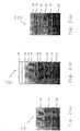
- the microstructure of the films were investigated by a Rigaku x-ray diffractometer with a Cu Ka radiation and a Philips EM420T transmission electron microscope.
- the x-ray diffractometer scans were all taken on a Rigaku Theta/ Theta Diffractometer operating at 35 kV and 20 ma with the Cu K alpha radiation from a target vacuum tube. The scans were taken in 0.05 degree steps, at two seconds per step.
- a series of slits were used to insure a parallel beam: the divergence and scatter slits used were one degree, and the receiving slit was 0.3 mm.
- a curved graphite monochrometer was used (radius of curvature: 224 mm) diffracting from the (0002) planes.
- the cross section of the x-ray beam is approximately 32 mm 2 . This procedure will be referred to herein as the thin film XRD method.
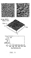
- the surfaces of the Ag thin films were examined with a Dimension 3000 atomic force microscope (AFM).
- the magnetic measurements were performed on a Digital Measurement Systems vibrating sample/torque magnetometer.
- XRD x-ray diffraction
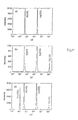
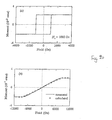
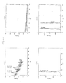
- Fig. 9(d) shows the surface root-mean-square roughness ( R rms ) vs. the film thickness, compared to a bare HF-etched Si surface R rms of about 4 ⁇ .
- R rms surface root-mean-square roughness
- a R rms of 57 ⁇ is found to be higher than the nominal film thickness.
- the surface roughness increases up to 104 ⁇ and becomes smaller as the film thickness on the 125 ⁇ Ag film.
- CoCrTa/Cr thin films of the same thicknesses grown on Ag templates of different thicknesses show much larger Cr(002) and CoCrTa(11 2 0) diffraction peaks than would normally be observed in the absence of the Ag underlayer template.
- good Ag/Si(001) epitaxy is achieved for all Ag film thicknesses, Fig. 10(a-b), the CoCrTa films deposited on Ag underlayers having a sufficient thickness to provide a continuous Ag template exhibited higher coercivities.
- the surface roughness of a 125 ⁇ thick Ag template is larger than that of a 50 ⁇ Ag film (the ratio of the R rms to the film thickness, however, is smaller), but the connected web-like surface structure seems to enhance the epitaxial growth and the coercivity of a CoCrTa(200 ⁇ )/Cr(300 ⁇ ) film when compared to the island structure.
- the decrease in coercivity on very thick Ag templates is also accompanied by significantly expanded Ag surface features.
- the growth of the Cr films on the Ag templates with different surface morphologies at different thicknesses appears to play a role in the magnetic properties of CoCrTa films.
- the web-like structure can be made more or less continuous resulting in a corresponding variation in the Co/Cr textures for differing film thicknesses.
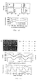
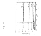
- Fig. 11(a) shows the Cr[001] zone axis electron diffraction pattern of a CoCrTa/Cr film, which agrees well with the simulated pattern in Fig. 11(b).
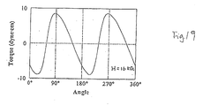
- the periodic variation of the magnetic properties shown in Fig. 11(c) is further evidence of the bicrystal nature of CoCrTa films. Also, a parallel relationship appears to exist between the Cr[100] and Si[110] directions. Furthermore, the periodicity of 90° in the in-plane torque curve (Fig. 11(d)) not only indicates a bicrystal structure, but also that the volume fractions of two CoCrTa orientation variants are almost equal.
- the thickness of the Ag template required to maximize coercivity and minimize the surface roughness using the current process is approximately 500-1000 ⁇ .
- the resulting Cr and Co layers are not respectively(110) and (10 1 1), as expected.
- the Cr epitaxially grows in a (112) orientation when deposited using the (110) orientation of the Ag layer as a template.
- the Co layer then epitaxially grows when deposited using the Cr (112) orientation as a template to produce a Co layer having the uni-crystal (10 1 0) orientation.
- the orientation having the lowest energy state is the (110) because of its closely packed atomic configuration.
- the orientation having the lowest energy state is the (110) because of its closely packed atomic configuration.
- the bcc (110) orientation there is a center atom (Fig. 6)
- the corresponding (110) fcc orientation there is no center atom (see Fig. 4).
- the lack of a center atom in the (110) fcc is believed to increase the energy state of the (110) bcc, thereby making it far less favorable when deposited on (110) Ag.
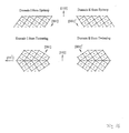
- the atomic structure of a bcc lattice is such that an atomic arrangement similar to the fcc (110) orientation is possible in the (112) plane, as shown in Fig. 6.
- One dimension in the (112) plane is the diagonal lattice face spacing and the other dimension is the closest packed distance between a corner atom and the center atom in the bcc structure, which is twice the atomic radii.
- the Cr (112) orientation can also be lattice matched along the Ag[110]
- the spacings of the atoms in the Cr (112) texture with the Ag (110) texture is not nearly as well matched as the Cr (110) unit cell dimensions.
- the absence of the center atom in the (112) orientation decrease its lattice energy state at the interface with the (110) fcc template such that it is less than the (110) orientation. Therefore, the bcc will epitaxially grow in the (112) orientation.
- a bcc (112) or a fcc (110) can be used to induce the (10 1 0) texture in a Co-based film, if the atomic spacings are compatible.
- (10 1 0) Co-based material should grow directly on the (110) fcc Ag in view of the similarity of the atomic spacings for (112) Cr and (10 1 0) Co.
- a controlled orientation recording media and transducer can be produced using a single crystal substrate, such as Si.
- the single crystal substrate can be used to epitaxially grow nearly ideal underlayers that culminate in a magnetic layer having an orientation of choice.
- a linearly addressed single crystal recording medium can be produced by employing the techniques described herein to produce a nearly ideal (112) bcc layer that will induce epitaxial growth of the (10 1 0) uni-crystal.
- the single crystal substrate propagates the single crystal structure through the underlayer structure to the magnetic layer structure.
- This combined with uni-directional orientation of the magnetic layer structure results in a recording medium or transducer in which the magnetic axis of each crystallite are parallel.
- the parallel alignment of the magnetic easy axes provides a linearly addressable recording medium that has little or no signal modulation.
- the oriented and aligned structure of the linear addressable recording medium provide the potential for lower media noise and increased coercivities that can theoretically reach H k .
- Cr to Ag -0.2% (along the Ag[001] direction) and 13.5% (perpendicular to the Ag[001] direction) on a one to one basis
- pure Co to Cr -0.5% (along the Co c-axis) and 0.4% (perpendicular to the Co c-axis).
- the mismatch of Cr to Ag perpendicular to the Ag[001] direction is approximately 1%, when the Cr is meshed with the Ag on a 7 to 3 ratio, or repeat unit.
- the (110) oriented Si single crystal substrate was prepared and the Ag, Cr, and Co (pure and alloy) thin films were then deposited sequentially by RF diode sputtering in a Leybold-Heraeus Z-400 sputtering system as previously discussed.
- the epitaxial orientation relationship of the layers was investigated using ⁇ / ⁇ and ⁇ -scan XRD with the Rigaku x-ray diffractometer with a Cu K ⁇ radiation.
- the magnetic properties and torque curves of the Co films were measured using the Digital Measurement Systems vibrating sample/torque magnetometer. From the torque curves of a uni-crystal Co film, the uniaxial anisotropy constants of the material can be determined.
- Fig. 13 The relative relationship of the vector and angular quantities used in equation (1) are shown in Fig. 13.
- the ⁇ / ⁇ XRD spectra for representative Ag, Cr/Ag, and Co/Cr/Ag films grown on HF-Si(110) are shown in Fig. 14(a-c), respectively. Only strong Ag(220), Cr(112) and Co(10 1 0) diffraction peaks are observed in these spectra, which strongly implies the epitaxial nature of these films.
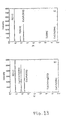
- the ⁇ -scan spectra of the Co/Cr/Ag/HF-Si sample are shown in Fig. 15, along with cubic crystal (110), (112), and Co (10 1 0) stereographic projections that are necessary for the interpretation of the spectra.
- Fig. 15(a') two diffraction peaks that are 180° apart are found in the Si ⁇ 004 ⁇ -pole scan spectrum for the single crystal Si(110) substrate (Fig. 15(a)).
- the two peaks corresponding to the Ag ⁇ 004 ⁇ poles are also 180° apart (Fig. 15(b)), which is in good agreement with the stereographic projection, Fig. 15(b'), and they appear at the same ⁇ positions as the two peaks in Si ⁇ 004 ⁇ -pole spectrum, confirming the parallel relationship between the Si[001] and Ag[001] directions.
- the Cr ⁇ 110 ⁇ -pole spectrum (Fig. 15(c)) contains two peaks that are again 180° apart in agreement with the projection in Fig. 15(c'). The peak locations are shifted by 90° when compared to the two peaks in Ag ⁇ 110 ⁇ -pole scan, indicating that the Cr[1 1 0] direction is parallel to the Ag[001] direction.
- the (112) stereographic projection of the crystal in Fig. 15(c') only shows one (001) pole.
- Two diffraction peaks, however, are observed in the Cr ⁇ 002 ⁇ -pole scan, indicating an extra pole as denoted by (001)' in Fig. 15(c').
- the two domains may emerge from the Cr/Ag epitaxial interface when Cr starts to grow with two different atomic configurations that are mirror images of each other.
- the two domains may also be a result of the Cr growth twinning.
- the (112) plane is the most common twinning plane, and the twinning direction is [11 1 ], as shown in Fig. 16.
- the resulting two domains of Cr grains have (112) planes parallel with the substrate plane, yet the atomic configurations are mirror images about the plane perpendicular to the twinning direction.
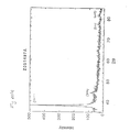
- the torque curve of the pure Co sample is shown in Fig. 17. It resembles a skewed sinusoidal curve'with a period of 180°.
- the anisotropy constants determined from the curve are smaller than the values reported for bulk Co single crystals (4.2-4.5 x 10 6 ergs/cm 3 ).
- the amplitude of the torque measurement indicates good alignment of the Co grain easy axes.
- K 1 was found to increase in pure Co films prepared at increasing substrate bias, as shown in Table I, which may indicate the presence of fcc stacking faults in an otherwise hcp Co crystalline structure.
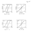
- Hysteresis loops for the samples were measured with the applied field along either the easy axis direction or the hard axis direction (see Figure 18).
- a square shape loop is observed along the easy axis with a coercivity around 200 Oe, indicating a coercivity mechanism associated with wall motion.
- the hard axis loop falls almost perfectly on the open circles indicating excellent agreement with the calculated points using the anisotropy constants determined from the torque measurements.
- a uni-crystal Co 84 Cr 13 Ta 3 /Cr/Ag/HF-Si(110) film was also prepared.
- a substrate bias of -170 V was applied during the deposition of the CoCrTa film.
- the anisotropy constants determined from the torque curve are also listed in Table I.
- Hysteresis loops for this sample are shown in Figure 20. For the very square easy axis hysteresis loop a coercivity of 1080 Oe is obtained while the linear behavior of the hard axis loop implies a reduced K 2 , in agreement with the torque analysis.
- the growth of the uni-crystal Co, Cr (112) and Ag (110) layers is similar to the growth described with respect to the Ag (001), Cr (001), and Co (11 2 0) layers described above. Therefore, a continuous Ag template is desired to maximize coercivity and minimize the surface roughness
- the (111) fcc provides a face with a triangular atomic structure upon which a subsequent layer can be epitaxially grown.
- the (111) orientation of the bcc layer also provide a triangular atomic structure.
- the bcc layer does not develop a (111) orientation when deposited upon the (111) fcc layer, but instead develops a (110) crystalline texture.
- the (110) bcc face has a rectangular shaped atomic structure with a center atom.
- the (110) orientation represents the lowest energy state for the bcc layer.
- Perpendicular recording is a promising candidate for future high density magnetic data storage, and Co-based alloy thin films are, by far, the most widely studied perpendicular media for future hard disks.
- the perpendicular c axis orientation of Co grains and high coercivity are two of the key factors to achieving a uni-crystal and low noise recording performance at high densities. Because most perpendicular recording transducers have very limited, non-sharp, head field gradients the recorded transition tends to be non-sharp.
- the perpendicular media is extremely highly oriented with virtually no dispersion in the c axes of the Co crystallites, then this can compensate for the less than ideal record head field gradients. Therefore, it is desirable to produce a highly oriented (0002) perpendicular Co layer for use in perpendicular recording media.
- the (0002) orientation provides a close packed atomic surface and is the lowest energy state for the hcp structure. Therefore, Co-based materials tend to naturally grow with a weak (0002) texture if there is no epitaxial interface to induce a different orientation (texture) upon the material.
- Previous studies have also attempted to use Ti to induce higher quality (0002) texture in the Co layer.
- the Ti layer is generally not well oriented. Thus, it can be inferred that Ti is not acting as a seed layer, but essentially as a wetting layer that eliminates the influence of the orientation of the substrate or previously deposited layer under the Co-based layer.
- the deposition of Co-based materials directly upon a fcc structure will generally result in a Co-based material developing a fcc structure and the orientation of the prior fcc layer.
- fcc structures are in the lowest energy state, therefore, the Co-based layers are likely to develop a strong fcc (111) crystallographic texture, which due to the cubic structure results in a low coercivity magnetic film.
- the particular compositions used in the fcc and hcp template layers will necessarily depend upon the lattice spacing of the desired magnetic layer.
- the hcp template layer must have a lattice spacing that is compatible with the fcc layer and should not have a stable fcc phase in the range of deposition temperatures and processing conditions.
- different composition can be used as the hcp template underlayer to vary the lattice size of the hcp template.
- the nearly ideal (111) fcc template can also be used to induce the epitaxial growth of other fcc structures analogous to the growth of the fcc Co layer.
- soft magnetic materials such as Ni and NiFe permalloys, can be epitaxially grown on the fcc template.
- the magnetic easy axes lie near the (111) plane; therefore, the soft magnetic layer will provide a close to in-plane return path for the magnetic field generated perpendicular to the layer during perpendicular recording.
- the soft magnetic materials can propagate the (111) orientation for the (0002) hcp template and (0002) hcp Co-based layers.
- a (0002) Co-based layer provides a template that will further induce soft magnetic materials to grow epitaxially in a (111) orientation to form a thin top keeper layer for the perpendicular media. It is noted that the keeper layer will also have the magnetically easy axes predominately in the plane of the layers.
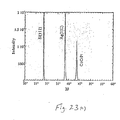
- Fig. 23(a) The x-ray diffraction spectra for a representative CoCrPt(50nm)/Ti(50nm)/Ag(12nm) film grown on HF-Si(111) are shown in Fig. 23(a). Only those peaks corresponding to CoCrPt(0002), Ti(0002), and Ag(111) planes are observed in these spectra, indicating a good orientation of the films. As a comparison, CoCrPt(50nm)/Ti(50nm) films were also grown directly on HF-Si(111) without the thin Ag template and the x-ray spectrum in Fig. 23(b) shows a good, but weaker Ti(0002) peak.
- Fig. 24 shows the ⁇ -scan spectra of the CoCrPt/Ti/Ag/HF-Si sample and samples with fewer layers, along with cubic crystal (111) and Co (0001) stereographic projections that are necessary for the interpretation of the spectra.
- (111) stereographic projection Fig. 24(a')
- three diffraction peaks that are 120° apart are found in the Si ⁇ 220 ⁇ -pole scan spectrum for the single crystal Si(111) substrate (Fig. 24(a)).
- the (111) stereographic projection of cubic crystal in Fig. 24(b') (Ag/HF-Si) only shows three (110) poles. Six diffraction peaks, however, are observed in the Ag ⁇ 220 ⁇ -pole scan, indicating extra poles as denoted by crosses in Fig. 24(b'). This suggests that there exist two crystallographic domains of Ag grains in the Ag(111) film. The two domains most likely emerge from the Ag/Si epitaxial interface when Ag starts to grow with two different atomic configurations that are mirror images of each other. The two domains may also be a result of the Ag growth twinning. In fcc metals, the (111) plane is the most common twinning plane, and the twinning direction is [11 2 ].
- the resulting two domains of Ag grains have (111) planes parallel with the substrate plane, yet the atomic configurations are mirror images about the plane perpendicular to the twinning direction.
- the first, third and fifth peaks in the Ag ⁇ 220 ⁇ -pole scan spectrum appear at the same locations as the three peaks in Si ⁇ 220 ⁇ scan, confirming the parallel relationship between the Si[11 2 ] and Ag[11 2 ] directions.
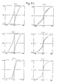
- the magnetic properties of the CoCrPt/Ti/Ag/HF-Si(111) sample are compared to those of four other samples as listed in Table II.
- the coercivities ( H c ⁇ ) were measured with the applied field perpendicular to the film planes.
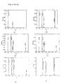
- Figs. 25(a1-e1) and (a2-e2) show the perpendicular(easy axis) and in-plane(hard axis) hysteresis loops of samples A-E, respectively.
- a skewed square loop is observed along the perpendicular direction due to the demagnetization field.
- the openness and the non-zero coercivity in the hard axis in-plane loop may be due to intergranular interactions or simply that the maximum applied field intensity is insufficient to saturate the samples.
- the curvature of the hard axis loop is most likely due to the non-zero value of the anisotropy constant K 2 as discussed earlier with respect to the Co(10 1 0) films.
- samples A and B are CoCrPt/Ti films deposited on a glass substrate and a Si(111) wafer covered with native oxide, respectively.
- the XRD spectra of the samples do not show a Ti crystal texture in either both samples, as previously discussed.
- the coercivities of samples A and B are low, presumably because the Co layer did not epitaxially grow in the (0002) orientation, but slowly developed some (0002) texture naturally as the films became thicker, which resulted in dispersion in the c axis orientation.
- the poorer orientation is also indicated by the shape of the hysteresis loops shown in Figs. 25(a1-b1) and (a2-b2).
- Sample E was prepared by depositing a 50nm CoCrPt film directly on a 50nm Ag underlayer on HF-Si(111) and tested for comparison with the CoCrPt/Ti/Ag/Si films.
- the hysteresis curves for Sample E are shown in Figs. 25(el and e2).
- the XRD spectra (Fig. 23(c)) shows an extremely strong crystal texture for the CoCrPt film.
- the coercivity of sample E is low compared with samples grown on Ti either with or without the Ag indicating that the Co phase is most likely present as an fcc structure.
- fcc templates and underlayers can also be used to improve the lattice matching of the films.
- Cu has an atomic lattice spacing that is compatible with the lattice spacing of Co and to a lesser extent with Ag.
- a Co(1000 ⁇ )/Cu (500 ⁇ )/Ag(300 ⁇ )/Si (111) film was prepared and tested. As shown in Fig. 26(a), both the Cu (111) and the Co (0002) layer show exceptionally strong epitaxial growth from the Ag (111) template. In contrast, the Cu atomic lattice spacing is generally less compatible with that of the Si.
- a Co(1000 ⁇ )/Cu (500 ⁇ )/Si (111) film does not result in a strong texture in either the Cu or the Co layer, as shown in Fig. 26(b).
- NiFe with a (111) texture it is generally desirable to prepare NiFe with a (111) texture to enable very soft magnetic properties.
- permalloys and other soft magnetic material can be produced in (111) orientation that will result in three fold oriented, magnetic easy (111) axes lying near the substrate plane.
- perpendicular media can be produced with a soft magnetic underlayer and/or even a soft overlayer (keepered media).
- keepered media For example:
- Permalloy (Ni 79 wt%, Fe 21 wt%) films were sputter deposited on different underlayers on HF cleaned Si(111) substrates using the techniques previously described, except that the films were heated to 260°C prior to deposition.
- the composition of the permalloy film are shown below in Table III: Sample Configuration A NiFe 50nm/ Si(111)-HF B NiFe 50nm/ Ag 100nm/Si(111)-HF C NiFe 50nm/Cu 10nm/Ag 100nm/Si(111)-HF D NiFe 50nm/Cu 50nm/Ag 100nm/Si(111)-HF E NiFe 50nm/Cu 100nm/Ag 100nm/Si(111)-HF F NiFe 50nm/Cu 100nm/Ag 100nm/Si(100)-HF
- Figs. 27(a-f) The XRD spectra for each film is shown in Figs. 27(a-f).
- the NiFe develops only weak (111) texture when deposited on (111) Si.
- the deposition of a fcc (111) Ag template underlayer on the (111) Si prior to the deposition of the permalloy produces strong (111) texture development in the NiFe layer, as evidenced by the factor of 20 increase in the counts detected during XRD testing.
- the Cu underlayer further increases the (111) texture of the NiFe film.
- NiFe(100) has also been deposited on Cu/Ag/Si(100)-HF single crystal template for comparison with the NiFe (111) texture.
- the magnetic properties have been characterized with BH loop tracer.
- the in-plane coercivity of samples E and F were determined and are shown below: Sample Maximum in-plane Hc Minimum in-plane Hc E 2.64 Oe 1.65 Oe F 26.5 Oe 18.6 Oe
- the coercivity of NiFe(111) along an easy axis of the Cu/Ag/Si(111) template is less than 3 Oe, whereas, the in-plane coercivity of NiFe(100) film on Cu/Ag/Si(100) template is nearly 30 Oe.
- the coercivity will be further reduced.
- a soft magnetic keeper layer on top of the Co-alloy, such as NiFe(111)/Cu(111)/Ag(111)/CoCrPtTa(0002)/Ti(0002) /Ag(111)/NiFe(111)/Cu(111)/Ag(111)/HF-Si(111).
- (111) fcc structure can also be produced using a lattice matched (110) bcc structure, in lieu of the nearly ideal (111) single crystal Si.
- the strength of the (111) texture will depend upon the strength of the (110) texture.
- the Ag (111) can be grown on a (110) textured Cr or CrMn with a strong (111) texture, which, in turn, can be used to grow strongly textured (111) NiFe or (110) bcc, (0002) or (10 1 1) Co-based layers as previously described.
- reasonable quality (110) bcc textures can be obtained due to the atomic close packed surface structures, several high quality textures can be obtained upon these layers.
- polycrystalline uni-crystal cobalt can be induced via proper lattice compatibility of the Co(10 1 0)/bcc(112)/fcc(110)/bcc(110) layers, or even Co(10 1 0)/bcc(112)/bcc(110).
- (110) bcc and bcc derivatives with unit cell lattice parameters of a ⁇ 5.0 (Ba, BaCa, etc.), a ⁇ 3.5 (La, ⁇ -Zr) or a ⁇ 3.75 (LaZn, LaAg, NdAl, CeAg) are suitable matches to a fcc (110) structures, such as Ni, Co, and Cu, and (110) bcc structures with a ⁇ 5.7 (Rb) match reasonably to Ag(110) to yield:
- Figs. 28(a-b) show x-ray diffraction spectra of various Ag(111) underlayer films grown on glass substrates without and with a (110) CrMn underlayer.
- the low energy (111) orientation of the fcc structure is the predominant orientation, but the (111) texture is weak and other orientations are also observed in the spectra.
- Fig. 28(b) shows the Ag(111) texture on the CrMn layer to be strongly developed, nearly seven times the intensity of the (111) texture without the bcc layer.
- Figs. 29(a) and (b) show XRD spectra for a NiFe 50 nm film deposited directly on a glass substrate and on a Cu film deposited on a glass substrate at 260°C. As expected, neither film develops a strong texture and for the NiFe/glass film weak peaks are observed for both the (111) and (200) NiFe orientations.
- Figs. 29(c-d) show XRD spectra of a Cu(100nm)/Ag(100nm)/Cr(30 nm)/glass and Cu(100nm)/Cr(30 nm)/glass deposited at room temperature, which exhibit strong peaks indicative of a stong (111) texture in the films.
- the strength of the (111) texture in the Ag layer on the Cr/glass layers is less than on the single crystal Si (111).
- the use of the lattice matched bcc layer provides for increased flexibility in substrate selection and provides for a polycrystalline layer that can be used to induce, extremely strong (111) texture.
- Co-based layers that have a quad-crystalline (10 1 1) or (0002) perpendicular orientation can be produced on a conventional rotating recording medium, in which the crystals are random in the plane of the medium and have quad-crystalline or perpendicular order within the crystal.
- Fig. 30 shows the XRD scans of typical Cr films of various thicknesses prepared by RF diode sputtering on to glass substrates.
- the (110) peaks increase somewhat linearly with film thickness as more of the x-rays are diffracted from the thicker films as oppose to being transmitted.
- the peak to peak fluctuations or noise of the background signal is relatively constant. Comparing the (110) signal peak height of the 50 nm thick film to the peak to peak noise to one can see that the ratio is less than 10.
- one takes the signal peaks for the thicker films and divides by ratio of the film thickness to 50 nm one obtains about the same peak signal to noise ratio.
- the films of the present invention have XRD signal to noise ratios of at least 10 to 1 per 50 nm of film thickness as determined using the thin film XRD method described herein. While the present invention can be practiced using films having lower signal to noise ratios, the benefit of the invention will most likely not be realized to the same extent as for those films having higher ratios.
- the use of the bcc (110) layer to induce the (111) fcc layer provides for Co-based layers having a strong (0002) orientation that can be incorporated into conventional magnetic media for use in perpendicular recording applications employing straight forward underlayer and magnetic structures, such as CoCrPtTa(0002)/Ti(0002)/Ag(111)/Cr(110)/glass). These layers should be useful in both magneto-optic media and perpendicular magnetic media with and without the soft underlayer structures and the keeper media overlayers.
- the Cr alloy films with (110) texture are generally easy to achieve because the (110) texture surface is the lowest energy, close packed, surface for the bcc crystal. It has been shown that Cr(110) can be prepare by depositing very thick layers, depositing at room temperature, using low deposition rates, or most preferably by using substrate bias voltage during sputter deposition.
Abstract
Description
| quad-Crystal | Co(10 Co(10 |
| bi-Crystal | Co(11 Co(11 |
| uni-Crystal | Co(10 |

| Uniaxial Anisotropy Constants measured from torque curves | |||
| Substrate Bias(V) | K 1 (106 erg/cm3) | K 2 (106 erg/cm3) | |
| | 0 | 1.15 | 0.74 |
| Co | -100 | 1.42 | 0.89 |
| Co | -200 | 1.57 | 0.83 |
| Co | -300 | 2.22 | 0.78 |
| Co84Cr13Ta3 | -170 | 2.11 | 0.10 |
| Sample | Substrate | HC (Oe) | S | Mst (memu /cm2) | |
| (A) | CoCrPt 50nm/ Ti 50nm | Glass | 1928 | 0.82 | 2.5 |
| (B) | CoCrPt 50nm/ Ti 50nm | Non HF-etched Si(111) | 2514 | 0.83 | 2.5 |
| (C) | CoCrPt 50nm/ Ti 50nm | HF-Si(111) | 3550 | 0.96 | 2.5 |
| (D) | CoCrPt 50nm/ Ti 50nm/Ag 12nm | HF-Si(111) | 4580 | 0.85 | 2.5 |
| (E) | CoCrPt 50nm/ Ag 50nm | HF-Si(111) | 278 | 0.085 | 2.5 |
NiFe(111)/Cu(111)/Ag(111)/HF-Si(111) would provide both an oriented soft magnetic underlayer with a highly oriented perpendicular hard magnetic layer.
| Sample | Configuration |
| A | NiFe 50nm/ Si(111)-HF |
| B | NiFe 50nm/ Ag 100nm/Si(111)-HF |
| C | NiFe 50nm/Cu 10nm/Ag 100nm/Si(111)-HF |
| D | NiFe 50nm/Cu 50nm/Ag 100nm/Si(111)-HF |
| E | NiFe 50nm/Cu 100nm/Ag 100nm/Si(111)-HF |
| F | NiFe 50nm/Cu 100nm/Ag 100nm/Si(100)-HF |
| Sample | Maximum in-plane Hc | Minimum in-plane Hc |
| E | 2.64 Oe | 1.65 Oe |
| F | 26.5 Oe | 18.6 Oe |
a Co or Co alloy film having a (10
magnetic layer; and,
substrate having a (110) crystal texture; and,
said providing a first underlayer comprises growing a first underlayer having a (110) crystal texture on the substrate.
a first underlayer having a body centered cubic structure and a (110) crystal texture disposed between said substrate and said soft magnetic layer; and,
said first underlayer and said soft magnetic layer.
said substrate is a Si(111) single crystal.
a Co or Co alloy film having a (10
substrate and said magnetic recording layer and (ii) at least one second underlayer having a body centered cubic structure and a (110) crystal texture disposed between said first underlayer and said magnetic recording layer.
and said substrate is a Si(111) single crystal.
to 46, and,
a magnetic transducer positioned in close proximity to said
at least one first underlayer having a face entered cubic structure and a (111) crystal texture disposed between said substrate and said magnetic layeri and,
at least one second underlayer disposed between said first underlayer and said magnetic layer structure.
a first underlayer having a face centered cubic structure and a (111) crystal texture disposed between said substrate and said magnetic layer; and,
a second underlayer having a body centered cubic structure and a (110) crystal texture disposed between said first underlayer and said magnetic layer structure.
at least one first underlayer having a face centered cubic structure and a (110) crystal texture disposed between said substrate and said magnetic layer; and,
at least one second underlayer having a body centered cubic structure and a (112) crystal texture disposed between said first underlayer and said magnetic layer structure.
a Co or Co alloy film having a (10
a first underlayer having a face centered cubic structure and a (111) crystal texture disposed between said substrate and said magnetic recording layer; and,
a second underlayer having a body centered cubic structure and a (110) crystal texture disposed between said first underlayer and said magnetic recording layer.
Claims (25)
- A recording medium comprising:characterized in that the substrate is a single crystal Si having one of a (111) crystal texture, a (110) crystal texture or a (110) crystal texture and said underlayer is epitaxially grown on said substrate.an underlayer structure having at least one underlayer;a magnetic layer structure disposed on the underlayer structure; anda substrate disposed beneath the underlayer, the recording medium
- The recording medium of Claim 1 wherein said magnetic layer structure is comprised of ordered magnetic arrays.
- The recording medium recited in Claims 1 or 2 wherein the substrate is Si (111) and the underlayer structure is characterized by
at least one first underlayer having a face centered cubic structure and a (111) crystal texture disposed between said substrate and said magnetic layer; and
at least one second underlayer disposed between said first underlayer and said magnetic layer structure. - The recording medium recited in Claims 1 or 2 wherein the substrate is Si (110) and the underlayer structure is characterized by
a first underlayer having a face centered cubic structure and a (110) crystal texture disposed between said substrate and said magnetic layer; and
a second underlayer having a body centered cubic or a body centered cubic derivative structure and a (112) crystal texture disposed between said first underlayer and said magnetic layer structure. - The recording medium recited in Claims 1 or 2 wherein the substrate is Si (111) and the underlayer structure is characterized by
a first underlayer having a face centered cubic structure and a (111)) crystal texture disposed between said substrate and said magnetic layer; and
a second underlayer having a body centered cubic or a body centered cubic derivative structure and a (110) crystal texture disposed between said first underlayer and said magnetic layer structure. - The recording medium recited in Claims 1 or 2 wherein the substrate is Si (100) and the underlayer structure is characterized by
a first underlayer having a face centered cubic structure and a (100) crystal texture disposed between said substrate and said magnetic layer; and
a second underlayer having a body centered cubic or a body centered cubic derivative structure and a (100) crystal texture disposed between said first underlayer and said magnetic layer structure. - The recording medium recited in Claims 1 or 2 wherein the substrate is Si (110) and the underlayer structure is characterized by
at least one first underlayer having a face centered cubic structure and a (110) crystal texture disposed between said substrate and said magnetic layer; and
a second underlayer having a body centered cubic or a body centered cubic structure and a (112) crystal texture disposed between said substrate and said magnetic layer structure. - The recording medium recited in Claims 1 or 2 wherein the substrate is Si (111), the magnetic layer is a Co or Co alloy film having a (10
1 1) crystal texture, and the underlayer structure is characterized by
a first underlayer having a face centered cubic structure and a (111) crystal texture disposed between said substrate and said magnetic recording layer; and
a second underlayer having a body centered cubic structure and a (110) crystal texture disposed between said first underlayer and said magnetic recording layer. - The recording medium recited in any one of Claims 1 to 5 wherein said magnetic layer structure comprises a Co or Co alloy based material having a (0002) crystal texture.
- The recording medium recited in Claim 9 further comprising a third underlayer comprised of a hexagonal close packed structure having a (0002) crystal texture disposed between said second underlayer and said magnetic layer structure.
- The recording medium recited in any one of Claims 1, 2 or 6 wherein said magnetic layer structure comprises a Co or Co alloy based material having a (10
1 0) crystal texture. - The recording medium recited in any one of Claims 1, 2 or 6 wherein said magnetic layer structure comprises a Co or Co alloy based material having a (11
2 0) crystal texture. - The recording medium recited in any one of Claims 1 to 5 wherein said magnetic layer structure comprises a Co or Co alloy based material having a (10
1 1) crystal texture. - The recording medium recited in any one of the preceding Claims further comprising a soft magnetic keeper layer disposed on said magnetic layer structure.
- The recording medium recited in any one of claims 3 to 8 or any one of Claims 9 to 13 dependent thereon further comprising a soft magnetic keeper layer disposed between the first and second underlayers.
- The recording medium recited in any one of claims further comprising a soft magnetic keeper layer disposed between said substrate and said magnetic layer structure.
- A recording medium comprising:an underlayer structure having at least one underlayer; anda superlattice multilayer magnetic layer structure, the recording medium chracterized in that the substrate is a single crystal Si having one of a (111) crystal texture, a (100) crystal texture or a (110) crystal texture, and said underlayer is epitaxially grown on the single crystal Si substrate.
- The recording medium of Claim 17 wherein the underlayer structure is characterized by (i) at least one first underlayer having a face centered cubic structure and a (111) crystal texture, (ii) at least one second underlayer disposed on said first underlayer and having a face centered structure and a (111) crystal texture, (iii) a soft magnetic layer disposed on said second underlayer, and (iv) at least one third underlayer disposed on said soft magnetic layer and having one of a hexagonal close packed structure with a (0002) crystal texture or a face centered cubic stucture with a (111) crystal texture.
- The recording medium of Claim 18 wherein said first underlayer is Ag, said second underlayer is Cu, said soft magnetic layer is NiFe, said third underlayer is Ti having a hexagonal close pack structure, a non-magnetic CoCr alloy or Ag, and said substrate is Si (111).
- The recording medium of Claim 18 or 19 wherein said magnetic layer is selected from the group consisting of a Co and Pt multilayer, a Co and Pd multilayer and combinations thereof.
- An apparatus for data storage comprising:the recording medium recited in any of the prceding Claims; anda magnetic transducer positioned in close proximity to said medium to record and read data to and from said medium.
- A magneto-optic data storage device including the recording medium of any one of Claims 1 to 20.
- A transducer comprising:an underlayer structure having at least one underlayer;a magnetic layer structure disposed on the underlayer structure; anda substrate disposed beneath the underlayer structure chracterized in that the substrate is a single crystal Si having one of a (111) crystal texture, a (100) crystal texture, or a (110) crystal texture, and said underlayer is epitaxially grown on the single crystal Si substrate.
- The transducer of Claim 20 wherein said magnetic layer structure comprises a NiFe, Co or Co alloy based material having a face centered cubic (111) crystal texture.
- An apparatus for data storage comprising:the recording transducer recited in Claim 23 or Claim 24; anda magnetic medium positioned in close proximity to said transducer, wherein said transducer is sued to record and read data to and from said medium.
Applications Claiming Priority (3)
| Application Number | Priority Date | Filing Date | Title |
|---|---|---|---|
| US08/967,669 US6248416B1 (en) | 1997-11-10 | 1997-11-10 | Highly oriented magnetic thin films, recording media, transducers, devices made therefrom and methods of making |
| EP98959396A EP1031143B1 (en) | 1997-11-10 | 1998-11-09 | Highly oriented magnetic thin films, recording media, transducers, devices made therefrom and methods of making |
| US967669 | 2007-12-31 |
Related Parent Applications (1)
| Application Number | Title | Priority Date | Filing Date |
|---|---|---|---|
| EP98959396.7 Division | 1998-11-10 |
Publications (1)
| Publication Number | Publication Date |
|---|---|
| EP1310949A1 true EP1310949A1 (en) | 2003-05-14 |
Family
ID=25513142
Family Applications (5)
| Application Number | Title | Priority Date | Filing Date |
|---|---|---|---|
| EP03002412A Withdrawn EP1310948A1 (en) | 1997-11-10 | 1998-11-09 | Highly oriented magnetic thin films, recording media, transducers, devices made therefrom and methods of making |
| EP03001967A Withdrawn EP1308936A1 (en) | 1997-11-10 | 1998-11-09 | Highly Oriented Magnetic Thin Films, Recording Media, Transducers, Devices Made Therefrom and Methods of Making |
| EP03002413A Withdrawn EP1315152A1 (en) | 1997-11-10 | 1998-11-09 | Highly oriented magnetic thin films, recording media, transducers, devices made therefrom and methods of making |
| EP98959396A Expired - Lifetime EP1031143B1 (en) | 1997-11-10 | 1998-11-09 | Highly oriented magnetic thin films, recording media, transducers, devices made therefrom and methods of making |
| EP03002468A Withdrawn EP1310949A1 (en) | 1997-11-10 | 1998-11-09 | Highly orientated magnetic thin films, recording media, transducers, devices made therefrom and methods of making |
Family Applications Before (4)
| Application Number | Title | Priority Date | Filing Date |
|---|---|---|---|
| EP03002412A Withdrawn EP1310948A1 (en) | 1997-11-10 | 1998-11-09 | Highly oriented magnetic thin films, recording media, transducers, devices made therefrom and methods of making |
| EP03001967A Withdrawn EP1308936A1 (en) | 1997-11-10 | 1998-11-09 | Highly Oriented Magnetic Thin Films, Recording Media, Transducers, Devices Made Therefrom and Methods of Making |
| EP03002413A Withdrawn EP1315152A1 (en) | 1997-11-10 | 1998-11-09 | Highly oriented magnetic thin films, recording media, transducers, devices made therefrom and methods of making |
| EP98959396A Expired - Lifetime EP1031143B1 (en) | 1997-11-10 | 1998-11-09 | Highly oriented magnetic thin films, recording media, transducers, devices made therefrom and methods of making |
Country Status (9)
| Country | Link |
|---|---|
| US (1) | US6248416B1 (en) |
| EP (5) | EP1310948A1 (en) |
| JP (1) | JP2001523032A (en) |
| KR (1) | KR20010031782A (en) |
| CN (1) | CN1285948A (en) |
| DE (1) | DE69812689T2 (en) |
| HK (1) | HK1028130A1 (en) |
| TW (1) | TW418388B (en) |
| WO (1) | WO1999024973A1 (en) |
Families Citing this family (79)
| Publication number | Priority date | Publication date | Assignee | Title |
|---|---|---|---|---|
| US6764738B1 (en) * | 1998-02-10 | 2004-07-20 | Seagate Technology Llc | Magnetic recording medium with patterned substrate |
| US20040103422A1 (en) * | 1998-03-19 | 2004-05-27 | Seagate Technology Llc | Hybrid recording device (HRD) with magneto-resistance head on optically assisted media |
| JP2000099934A (en) * | 1998-09-25 | 2000-04-07 | Fujitsu Ltd | Magnetic recording medium and magnetic recording device |
| JP3665221B2 (en) * | 1999-03-18 | 2005-06-29 | 株式会社日立グローバルストレージテクノロジーズ | In-plane magnetic recording medium and magnetic storage device |
| JP3549429B2 (en) * | 1999-03-19 | 2004-08-04 | 富士通株式会社 | Magnetic recording medium and method for manufacturing the same |
| WO2000060583A1 (en) * | 1999-03-31 | 2000-10-12 | Hitachi, Ltd. | Magnetic recording medium and magnetic storage device |
| JP3864637B2 (en) * | 1999-10-05 | 2007-01-10 | 富士通株式会社 | Magnetic recording medium |
| JP2001143250A (en) * | 1999-11-12 | 2001-05-25 | Fujitsu Ltd | Magnetic memory medium and magnetic storage device |
| US6562489B2 (en) | 1999-11-12 | 2003-05-13 | Fujitsu Limited | Magnetic recording medium and magnetic storage apparatus |
| JP2001184626A (en) * | 1999-12-24 | 2001-07-06 | Hitachi Ltd | Magnetic recording medium and magnetic memory device |
| JP2001222809A (en) * | 2000-02-08 | 2001-08-17 | Toshiba Corp | Magnetic recording medium |
| JP2001344740A (en) * | 2000-05-26 | 2001-12-14 | Hitachi Ltd | Magnetic recording medium and magnetic storage device |
| US6423431B1 (en) * | 2000-05-30 | 2002-07-23 | Maxtor Corporation | Magnetic recording media having improved magnetic and parametric performance with chromium alloy underlayer having added aluminum |
| US6428906B1 (en) * | 2000-05-30 | 2002-08-06 | Maxtor Corporation | Magnetic recording media having a layered structure for perpendicular magnetization of a recording layer |
| US6838188B1 (en) * | 2000-05-30 | 2005-01-04 | Maxtor Corporation | Magnetic recording medium having ternary or quaternary alloy seedlayer |
| US6703099B2 (en) | 2000-07-27 | 2004-03-09 | Seagate Technology Llc | Perpendicular magnetic recording media with patterned soft magnetic underlayer |
| US6667118B1 (en) * | 2000-09-05 | 2003-12-23 | Seagate Technology Llc | Texture-induced magnetic anisotropy of soft underlayers for perpendicular recording media |
| JP3652976B2 (en) * | 2000-09-28 | 2005-05-25 | 株式会社日立製作所 | Perpendicular magnetic recording medium and magnetic storage device using the same |
| JP3762277B2 (en) * | 2000-09-29 | 2006-04-05 | キヤノン株式会社 | Magnetic recording medium and method for manufacturing the same |
| KR100714254B1 (en) | 2000-11-29 | 2007-05-02 | 후지쯔 가부시끼가이샤 | Textured magnetic recording medium with cr-based underlayer an co-based magnetic layer having special orientations |
| US6537638B2 (en) * | 2000-12-13 | 2003-03-25 | International Business Machines Corporation | Magnetic recording disk with perpendicular magnetic recording layer and multilayered underlayer structure |
| KR100374792B1 (en) * | 2000-12-29 | 2003-03-04 | 삼성전자주식회사 | Perpendicular magnetic recording disks |
| KR100374793B1 (en) * | 2001-01-03 | 2003-03-04 | 삼성전자주식회사 | Perpendicular magnetic recording media |
| US7050274B2 (en) | 2001-03-15 | 2006-05-23 | Seagate Technology Llc | Multilayer permanent magnet films |
| SG115476A1 (en) * | 2001-05-23 | 2005-10-28 | Showa Denko Kk | Magnetic recording medium, method of manufacturing therefor and magnetic replay apparatus |
| EP1435091B1 (en) | 2001-08-29 | 2014-07-16 | Lambeth Magnetic Structures, LLC | Magnetic material structures, devices and methods |
| JP4626840B2 (en) * | 2001-08-31 | 2011-02-09 | 富士電機デバイステクノロジー株式会社 | Perpendicular magnetic recording medium and manufacturing method thereof |
| JP4332833B2 (en) | 2001-08-31 | 2009-09-16 | 富士電機デバイステクノロジー株式会社 | Perpendicular magnetic recording medium and manufacturing method thereof |
| JP2003162806A (en) * | 2001-11-27 | 2003-06-06 | Hitachi Ltd | Perpendicular magnetic recording medium and magnetic storage device |
| JP4019703B2 (en) * | 2001-12-07 | 2007-12-12 | 富士電機デバイステクノロジー株式会社 | Perpendicular magnetic recording medium and manufacturing method thereof |
| JP4582978B2 (en) * | 2001-12-07 | 2010-11-17 | 富士電機デバイステクノロジー株式会社 | Method for manufacturing perpendicular magnetic recording medium |
| JP2003217107A (en) * | 2002-01-17 | 2003-07-31 | Fuji Electric Co Ltd | Magnetic recording medium |
| SG118182A1 (en) * | 2002-03-19 | 2006-01-27 | Fuji Electric Co Ltd | Method for producing a magnetic recording medium and a magnetic recording medium produced by the method |
| US6986954B2 (en) * | 2002-04-17 | 2006-01-17 | Imation Corp. | Perpendicular magnetic recording media |
| US6921585B2 (en) * | 2002-05-15 | 2005-07-26 | Imation Corp. | Perpendicular magnetic recording media with an amorphous underlayer |
| WO2004001779A1 (en) * | 2002-06-21 | 2003-12-31 | Seagate Technology Llc | Method of producing nife alloy films having magnetic anisotropy and magnetic storage media including such films |
| KR100803201B1 (en) * | 2002-07-27 | 2008-02-14 | 삼성전자주식회사 | Perpendicular magnetic recording media |
| US20040038082A1 (en) * | 2002-08-26 | 2004-02-26 | Toshihiro Tsumori | Substrate for perpendicular magnetic recording hard disk medium and method for producing the same |
| US7128988B2 (en) | 2002-08-29 | 2006-10-31 | Lambeth Systems | Magnetic material structures, devices and methods |
| JP2005526352A (en) * | 2002-09-06 | 2005-09-02 | 富士通株式会社 | Magnetic recording medium and magnetic storage device |
| US7449255B2 (en) | 2002-09-30 | 2008-11-11 | Seagate Technology Llc | High moment directionally textured soft magnetic underlayer in a magnetic storage medium |
| US6853519B2 (en) | 2002-10-17 | 2005-02-08 | International Business Machines Corporation | Magnetic head having high conductivity lead structures seeded by epitaxially matched seed layer |
| JP4136590B2 (en) * | 2002-10-23 | 2008-08-20 | キヤノン株式会社 | Alignment film, magnetic recording medium using alignment film, and magnetic recording / reproducing apparatus |
| DE10258860A1 (en) * | 2002-12-17 | 2004-07-15 | Robert Bosch Gmbh | Magnetoresistive layer system and sensor element with this layer system |
| US7247396B2 (en) * | 2003-01-30 | 2007-07-24 | Seagate Technology Llc | Highly oriented perpendicular magnetic recording media |
| US7211340B2 (en) * | 2003-01-30 | 2007-05-01 | Seagate Technology Llc | Thin film structures providing strong basal plane growth orientation and magnetic recording media comprising same |
| DE60313206T2 (en) * | 2003-02-20 | 2007-07-19 | Fujitsu Ltd., Kawasaki | VERTICAL MAGNETIC RECORDING MEDIUM |
| US20080226817A1 (en) * | 2003-05-30 | 2008-09-18 | Seagate Technology Llc | Tilted perpendicular magnetic recording media and method and apparatus therefor |
| US7175925B2 (en) * | 2003-06-03 | 2007-02-13 | Seagate Technology Llc | Perpendicular magnetic recording media with improved crystallographic orientations and method of manufacturing same |
| US20040247943A1 (en) * | 2003-06-03 | 2004-12-09 | Seagate Technology Llc | Perpendicular magnetic recording media with improved fcc Au-containing interlayers |
| US6953629B2 (en) * | 2003-06-30 | 2005-10-11 | Imation Corp. | NiCr and NiFeCr seed layers for perpendicular magnetic recording media |
| US7282278B1 (en) * | 2003-07-02 | 2007-10-16 | Seagate Technology Llc | Tilted recording media with L10 magnetic layer |
| SG109001A1 (en) * | 2003-07-10 | 2005-02-28 | Shinetsu Chemical Co | Substrate for magnetic recording medium |
| WO2005034096A1 (en) * | 2003-09-05 | 2005-04-14 | Seagate Technology Llc | Dual seed layer for recording media |
| KR100590530B1 (en) * | 2003-12-10 | 2006-06-15 | 삼성전자주식회사 | Perpendicular magnetic recording media |
| JP4435558B2 (en) * | 2003-12-24 | 2010-03-17 | ヒタチグローバルストレージテクノロジーズネザーランドビーブイ | Magnetic recording medium |
| US7167391B2 (en) * | 2004-02-11 | 2007-01-23 | Hewlett-Packard Development Company, L.P. | Multilayer pinned reference layer for a magnetic storage device |
| KR100624418B1 (en) * | 2004-02-25 | 2006-09-18 | 삼성전자주식회사 | Perpendicular magnetic recording media and method for manufacturing the same |
| JP2005251264A (en) * | 2004-03-02 | 2005-09-15 | Fuji Electric Holdings Co Ltd | Vertical magnetic recording medium and its manufacturing method |
| JP2005251266A (en) * | 2004-03-03 | 2005-09-15 | Shin Etsu Chem Co Ltd | Substrate for magnetic recording medium and its manufacturing method |
| US7102920B2 (en) * | 2004-03-23 | 2006-09-05 | Hewlett-Packard Development Company, L.P. | Soft-reference three conductor magnetic memory storage device |
| JP4585214B2 (en) * | 2004-03-25 | 2010-11-24 | 株式会社東芝 | Magnetic recording medium and magnetic recording / reproducing apparatus using the same |
| JP4436175B2 (en) * | 2004-04-05 | 2010-03-24 | 信越化学工業株式会社 | Single crystal Si substrate with metal plating layer |
| JP2006114610A (en) * | 2004-10-13 | 2006-04-27 | Toshiba Corp | Magnetoresistive element, magnetic head using the same, and magnetic reproducer |
| JP2006185489A (en) | 2004-12-27 | 2006-07-13 | Fujitsu Ltd | Magnetic recording medium and magnetic storage device |
| US20060291100A1 (en) * | 2005-06-23 | 2006-12-28 | Seagate Technology Llc | Thin film structure having a soft magnetic interlayer |
| US7541105B2 (en) * | 2006-09-25 | 2009-06-02 | Seagate Technology Llc | Epitaxial ferroelectric and magnetic recording structures including graded lattice matching layers |
| US8110299B2 (en) * | 2009-02-27 | 2012-02-07 | Seagate Technology Llc | Granular perpendicular media interlayer for a storage device |
| US7964013B2 (en) * | 2009-06-18 | 2011-06-21 | University Of Louisiana At Lafayette | FeRh-FePt core shell nanostructure for ultra-high density storage media |
| US20120044595A1 (en) * | 2010-08-23 | 2012-02-23 | Hitachi Global Storage Technologies Netherlands B.V. | Perpendicular magnetic recording medium (pmrm) and magnetic storage systems using the same |
| US8628867B2 (en) | 2010-09-30 | 2014-01-14 | Seagate Technology Llc | Patterned template with 1xN nucleation site to grain growth for uniform grain size recording media |
| KR101250256B1 (en) * | 2011-03-03 | 2013-04-03 | 성균관대학교산학협력단 | MANUFACTURING METHOD OF CoP ALLOY THIN FILM AND PERPENDICULAR MAGNETIC RECORDING MEDIUM |
| JP6073194B2 (en) * | 2013-07-03 | 2017-02-01 | 昭和電工株式会社 | Magnetic recording medium, magnetic storage device |
| KR20170064021A (en) * | 2015-11-30 | 2017-06-09 | 에스케이하이닉스 주식회사 | Electronic device |
| US10614953B2 (en) | 2016-01-12 | 2020-04-07 | University Of Florida Research Foundation, Inc. | Mitigation of contamination of electroplated cobalt-platinum films on substrates |
| JP6914663B2 (en) | 2017-02-07 | 2021-08-04 | 昭和電工株式会社 | Magnetic recording medium and magnetic storage device |
| US11183215B1 (en) | 2017-11-20 | 2021-11-23 | Seagate Technology Llc | Thin-film crystalline structure with surfaces having selected plane orientations |
| US11423928B1 (en) | 2018-01-19 | 2022-08-23 | Seagate Technology Llc | Processing for forming single-grain near-field transducer |
| WO2021056543A1 (en) | 2019-09-29 | 2021-04-01 | 续天曙 | Game device capable of generating a plurality of game results by betting |
Citations (4)
| Publication number | Priority date | Publication date | Assignee | Title |
|---|---|---|---|---|
| EP0526044A1 (en) * | 1991-07-30 | 1993-02-03 | Kabushiki Kaisha Toshiba | Magnetoresistance effect element |
| JPH08315326A (en) * | 1995-03-13 | 1996-11-29 | Toshiba Corp | Magnetoresistant head |
| US5582897A (en) * | 1993-09-10 | 1996-12-10 | Shin-Etsu Chemical Co., Ltd. | Magnetic recording medium |
| US5616218A (en) * | 1994-09-12 | 1997-04-01 | Matereials Research Corporation | Modification and selection of the magnetic properties of magnetic recording media through selective control of the crystal texture of the recording layer |
Family Cites Families (7)
| Publication number | Priority date | Publication date | Assignee | Title |
|---|---|---|---|---|
| US4652499A (en) | 1986-04-29 | 1987-03-24 | International Business Machines | Magnetic recording medium with a chromium alloy underlayer and a cobalt-based magnetic layer |
| US4902583A (en) | 1989-03-06 | 1990-02-20 | Brucker Charles F | Thick deposited cobalt platinum magnetic film and method of fabrication thereof |
| JPH05195118A (en) | 1992-01-24 | 1993-08-03 | Nkk Corp | Titanium stock for substrate of magnetic disk |
| WO1996032465A1 (en) * | 1995-04-10 | 1996-10-17 | Labatt Brewing Company Limited | Beer having increased light stability |
| US5800931A (en) * | 1994-09-29 | 1998-09-01 | Carnegie Mellon University | Magnetic recording medium with a MgO sputter deposited seed layer |
| US5693426A (en) * | 1994-09-29 | 1997-12-02 | Carnegie Mellon University | Magnetic recording medium with B2 structured underlayer and a cobalt-based magnetic layer |
| US5796560A (en) * | 1995-03-13 | 1998-08-18 | Kabushiki Kaisha Toshiba | Magnetoresistive head |
-
1997
- 1997-11-10 US US08/967,669 patent/US6248416B1/en not_active Expired - Lifetime
-
1998
- 1998-11-09 DE DE69812689T patent/DE69812689T2/en not_active Expired - Fee Related
- 1998-11-09 EP EP03002412A patent/EP1310948A1/en not_active Withdrawn
- 1998-11-09 EP EP03001967A patent/EP1308936A1/en not_active Withdrawn
- 1998-11-09 EP EP03002413A patent/EP1315152A1/en not_active Withdrawn
- 1998-11-09 KR KR1020007004848A patent/KR20010031782A/en not_active Application Discontinuation
- 1998-11-09 WO PCT/US1998/023855 patent/WO1999024973A1/en not_active Application Discontinuation
- 1998-11-09 EP EP98959396A patent/EP1031143B1/en not_active Expired - Lifetime
- 1998-11-09 JP JP2000519886A patent/JP2001523032A/en active Pending
- 1998-11-09 EP EP03002468A patent/EP1310949A1/en not_active Withdrawn
- 1998-11-09 CN CN98813018A patent/CN1285948A/en active Pending
- 1998-11-10 TW TW087118665A patent/TW418388B/en not_active IP Right Cessation
-
2000
- 2000-11-22 HK HK00107477A patent/HK1028130A1/en not_active IP Right Cessation
Patent Citations (4)
| Publication number | Priority date | Publication date | Assignee | Title |
|---|---|---|---|---|
| EP0526044A1 (en) * | 1991-07-30 | 1993-02-03 | Kabushiki Kaisha Toshiba | Magnetoresistance effect element |
| US5582897A (en) * | 1993-09-10 | 1996-12-10 | Shin-Etsu Chemical Co., Ltd. | Magnetic recording medium |
| US5616218A (en) * | 1994-09-12 | 1997-04-01 | Matereials Research Corporation | Modification and selection of the magnetic properties of magnetic recording media through selective control of the crystal texture of the recording layer |
| JPH08315326A (en) * | 1995-03-13 | 1996-11-29 | Toshiba Corp | Magnetoresistant head |
Also Published As
| Publication number | Publication date |
|---|---|
| TW418388B (en) | 2001-01-11 |
| DE69812689T2 (en) | 2004-03-04 |
| CN1285948A (en) | 2001-02-28 |
| EP1315152A1 (en) | 2003-05-28 |
| EP1031143A1 (en) | 2000-08-30 |
| EP1308936A1 (en) | 2003-05-07 |
| JP2001523032A (en) | 2001-11-20 |
| EP1031143B1 (en) | 2003-03-26 |
| KR20010031782A (en) | 2001-04-16 |
| WO1999024973A1 (en) | 1999-05-20 |
| HK1028130A1 (en) | 2001-02-02 |
| EP1310948A1 (en) | 2003-05-14 |
| DE69812689D1 (en) | 2003-04-30 |
| US6248416B1 (en) | 2001-06-19 |
Similar Documents
| Publication | Publication Date | Title |
|---|---|---|
| EP1031143B1 (en) | Highly oriented magnetic thin films, recording media, transducers, devices made therefrom and methods of making | |
| EP0704839B1 (en) | Magnetic recording medium with B2 structured underlayer and a cobalt-based magnetic layer | |
| US5993956A (en) | Manganese containing layer for magnetic recording media | |
| US5800931A (en) | Magnetic recording medium with a MgO sputter deposited seed layer | |
| US7736769B2 (en) | Magnetic recording medium, method of producing the same, and magnetic storage apparatus | |
| EP1515311A1 (en) | Magnetic recording medium, magnetic storage apparatus and recording method | |
| EP1275110B1 (en) | Magnetic recording medium | |
| Grundy | Thin film magnetic recording media | |
| EP0140513A1 (en) | Thin film magnetic recording structures | |
| US6432563B1 (en) | Zinc enhanced hard disk media | |
| US7521136B1 (en) | Coupling enhancement for medium with anti-ferromagnetic coupling | |
| US6740397B1 (en) | Subseedlayers for magnetic recording media | |
| US20060177701A1 (en) | Magnetic recording medium, method of producing the same, and magnetic storage apparatus | |
| US6649277B1 (en) | Structure for and method of making magnetic recording media | |
| Wierman et al. | Noise characteristics in exchange-biased soft underlayers for perpendicular media | |
| US6596417B1 (en) | Magnetic recording medium with a Ga3Pt5 structured underlayer and a cobalt-based magnetic layer | |
| US20030124389A1 (en) | Magnetic recording medium, method of producing magnetic recording medium and storage apparatus | |
| Lambeth | Modern Hard Disk Media Issues | |
| Glijer et al. | Advanced multilayer thin films for ultra-high density magnetic recording media | |
| Bian et al. | Oriented longitudinal media on glass substrates | |
| Lodder | Information Storage Material, Magnetic | |
| Liu | Reduced exchange coupling in perpendicular multilayers | |
| Grundy | Microstructure and Coercivity in Thin Films and Multilayers | |
| SELLMYER | PHYSICS AND APPLICATIONS OF COMPLEX NANOMAGNETIC MATERIALS DJ SELLMYER, ZS SHAN, SS MALHOTRA, I. AL-OMARI Y. LIU, EW SINGLETON, AND SH LIOU | |
| JP2000163734A (en) | Magnetic recording medium and magnetic recording reproducing device |
Legal Events
| Date | Code | Title | Description |
|---|---|---|---|
| PUAI | Public reference made under article 153(3) epc to a published international application that has entered the european phase |
Free format text: ORIGINAL CODE: 0009012 |
|
| 17P | Request for examination filed |
Effective date: 20030205 |
|
| AC | Divisional application: reference to earlier application |
Ref document number: 1031143 Country of ref document: EP Kind code of ref document: P |
|
| AK | Designated contracting states |
Designated state(s): DE FR GB IE IT NL SE |
|
| AKX | Designation fees paid |
Designated state(s): DE FR GB IE IT NL SE |
|
| 17Q | First examination report despatched |
Effective date: 20040503 |
|
| STAA | Information on the status of an ep patent application or granted ep patent |
Free format text: STATUS: THE APPLICATION IS DEEMED TO BE WITHDRAWN |
|
| 18D | Application deemed to be withdrawn |
Effective date: 20041115 |
|
| REG | Reference to a national code |
Ref country code: HK Ref legal event code: WD Ref document number: 1053901 Country of ref document: HK |