EP1310811A2 - Optical device, enclosure and method of fabricating - Google Patents
Optical device, enclosure and method of fabricating Download PDFInfo
- Publication number
- EP1310811A2 EP1310811A2 EP02020396A EP02020396A EP1310811A2 EP 1310811 A2 EP1310811 A2 EP 1310811A2 EP 02020396 A EP02020396 A EP 02020396A EP 02020396 A EP02020396 A EP 02020396A EP 1310811 A2 EP1310811 A2 EP 1310811A2
- Authority
- EP
- European Patent Office
- Prior art keywords
- optical
- lid
- substrate
- base
- enclosure
- Prior art date
- Legal status (The legal status is an assumption and is not a legal conclusion. Google has not performed a legal analysis and makes no representation as to the accuracy of the status listed.)
- Granted
Links
Images



Classifications
-
- G—PHYSICS
- G02—OPTICS
- G02B—OPTICAL ELEMENTS, SYSTEMS OR APPARATUS
- G02B6/00—Light guides; Structural details of arrangements comprising light guides and other optical elements, e.g. couplings
- G02B6/24—Coupling light guides
- G02B6/42—Coupling light guides with opto-electronic elements
- G02B6/4201—Packages, e.g. shape, construction, internal or external details
- G02B6/4249—Packages, e.g. shape, construction, internal or external details comprising arrays of active devices and fibres
-
- G—PHYSICS
- G02—OPTICS
- G02B—OPTICAL ELEMENTS, SYSTEMS OR APPARATUS
- G02B6/00—Light guides; Structural details of arrangements comprising light guides and other optical elements, e.g. couplings
- G02B6/24—Coupling light guides
- G02B6/26—Optical coupling means
- G02B6/32—Optical coupling means having lens focusing means positioned between opposed fibre ends
-
- G—PHYSICS
- G02—OPTICS
- G02B—OPTICAL ELEMENTS, SYSTEMS OR APPARATUS
- G02B6/00—Light guides; Structural details of arrangements comprising light guides and other optical elements, e.g. couplings
- G02B6/24—Coupling light guides
- G02B6/42—Coupling light guides with opto-electronic elements
- G02B6/4201—Packages, e.g. shape, construction, internal or external details
-
- G—PHYSICS
- G02—OPTICS
- G02B—OPTICAL ELEMENTS, SYSTEMS OR APPARATUS
- G02B6/00—Light guides; Structural details of arrangements comprising light guides and other optical elements, e.g. couplings
- G02B6/24—Coupling light guides
- G02B6/36—Mechanical coupling means
- G02B6/3628—Mechanical coupling means for mounting fibres to supporting carriers
- G02B6/3648—Supporting carriers of a microbench type, i.e. with micromachined additional mechanical structures
- G02B6/3652—Supporting carriers of a microbench type, i.e. with micromachined additional mechanical structures the additional structures being prepositioning mounting areas, allowing only movement in one dimension, e.g. grooves, trenches or vias in the microbench surface, i.e. self aligning supporting carriers
-
- G—PHYSICS
- G02—OPTICS
- G02B—OPTICAL ELEMENTS, SYSTEMS OR APPARATUS
- G02B6/00—Light guides; Structural details of arrangements comprising light guides and other optical elements, e.g. couplings
- G02B6/24—Coupling light guides
- G02B6/36—Mechanical coupling means
- G02B6/3628—Mechanical coupling means for mounting fibres to supporting carriers
- G02B6/3684—Mechanical coupling means for mounting fibres to supporting carriers characterised by the manufacturing process of surface profiling of the supporting carrier
- G02B6/3692—Mechanical coupling means for mounting fibres to supporting carriers characterised by the manufacturing process of surface profiling of the supporting carrier with surface micromachining involving etching, e.g. wet or dry etching steps
-
- G—PHYSICS
- G02—OPTICS
- G02B—OPTICAL ELEMENTS, SYSTEMS OR APPARATUS
- G02B6/00—Light guides; Structural details of arrangements comprising light guides and other optical elements, e.g. couplings
- G02B6/24—Coupling light guides
- G02B6/36—Mechanical coupling means
- G02B6/3628—Mechanical coupling means for mounting fibres to supporting carriers
- G02B6/3684—Mechanical coupling means for mounting fibres to supporting carriers characterised by the manufacturing process of surface profiling of the supporting carrier
- G02B6/3696—Mechanical coupling means for mounting fibres to supporting carriers characterised by the manufacturing process of surface profiling of the supporting carrier by moulding, e.g. injection moulding, casting, embossing, stamping, stenciling, printing, or with metallic mould insert manufacturing using LIGA or MIGA techniques
-
- G—PHYSICS
- G02—OPTICS
- G02B—OPTICAL ELEMENTS, SYSTEMS OR APPARATUS
- G02B6/00—Light guides; Structural details of arrangements comprising light guides and other optical elements, e.g. couplings
- G02B6/24—Coupling light guides
- G02B6/42—Coupling light guides with opto-electronic elements
- G02B6/4201—Packages, e.g. shape, construction, internal or external details
- G02B6/4219—Mechanical fixtures for holding or positioning the elements relative to each other in the couplings; Alignment methods for the elements, e.g. measuring or observing methods especially used therefor
- G02B6/422—Active alignment, i.e. moving the elements in response to the detected degree of coupling or position of the elements
- G02B6/4221—Active alignment, i.e. moving the elements in response to the detected degree of coupling or position of the elements involving a visual detection of the position of the elements, e.g. by using a microscope or a camera
- G02B6/4224—Active alignment, i.e. moving the elements in response to the detected degree of coupling or position of the elements involving a visual detection of the position of the elements, e.g. by using a microscope or a camera using visual alignment markings, e.g. index methods
-
- G—PHYSICS
- G02—OPTICS
- G02B—OPTICAL ELEMENTS, SYSTEMS OR APPARATUS
- G02B6/00—Light guides; Structural details of arrangements comprising light guides and other optical elements, e.g. couplings
- G02B6/24—Coupling light guides
- G02B6/42—Coupling light guides with opto-electronic elements
- G02B6/4201—Packages, e.g. shape, construction, internal or external details
- G02B6/4219—Mechanical fixtures for holding or positioning the elements relative to each other in the couplings; Alignment methods for the elements, e.g. measuring or observing methods especially used therefor
- G02B6/4228—Passive alignment, i.e. without a detection of the degree of coupling or the position of the elements
- G02B6/423—Passive alignment, i.e. without a detection of the degree of coupling or the position of the elements using guiding surfaces for the alignment
- G02B6/4231—Passive alignment, i.e. without a detection of the degree of coupling or the position of the elements using guiding surfaces for the alignment with intermediate elements, e.g. rods and balls, between the elements
-
- G—PHYSICS
- G02—OPTICS
- G02B—OPTICAL ELEMENTS, SYSTEMS OR APPARATUS
- G02B6/00—Light guides; Structural details of arrangements comprising light guides and other optical elements, e.g. couplings
- G02B6/24—Coupling light guides
- G02B6/42—Coupling light guides with opto-electronic elements
- G02B6/4201—Packages, e.g. shape, construction, internal or external details
- G02B6/4256—Details of housings
Definitions
- the present invention relates to optical communication devices, and more particularly enclosures for optical communications devices that provide alignment between the optical communications device and an optical cable.
- An optical interconnect module is an optical-electrical device that enables an interface between optical communications systems and electrical communications systems.
- One or multiple optical fibers, bundled in an optic cable, are connected to the interconnect module to communicate with optical-electrical components of the interconnect module.
- the optical-electrical components interface data transmitted on the optical fibers to electrical communication systems or interface electrical communications systems to optical communications systems.
- An optical cable may need to be repeatedly connected and disconnected from the optical interconnect module. Because the optical fibers are generally very small, the alignment tolerance required to ensure that the fibers align with their respective optical and optical-electrical components is a few microns or less. The alignment tolerance must be reliably and repeatable achieved each time the optical fiber is reconnected to the optical interconnect module.
- an optical interconnect module 10 typically has a lid portion 12 and a base portion 14 which form the enclosure.
- the lid 12 joins with the base 14 to enclose and protect optical and optical-electrical components 22 (eg. an electro-optical transducer) from the exterior surrounding environment.
- Focusing elements 24 reside on the lid 12 to focus light from each optical fiber onto optical-electrical components 22 or light from the optical-electrical components 22 into an optical fiber.
- a ferrule 17 on the end of the optical cable 16 secures the optical cable to the lid 12 and aligns the optical fibers with their respective focusing elements 24.
- the ferrule 17 must be precisely positioned on the lid 12 so that the optical fibers align with their respective focusing elements 24, and the lid 12 must be precisely aligned with the base 14 so that focusing elements 24 are aligned with their respective optical-electrical components 22.
- guide pins 26 are received in pin retaining receptacles 28 of the base 14.
- the pin retaining receptacles 28 are positioned in precise relation to the optical-electrical components 22.
- the lid 12 has corresponding alignment apertures 30 through which pins 26 pass as the lid 12 is placed on base 14.
- the corresponding alignment apertures 30 are positioned in precise relation to focusing elements 24, so that focusing elements 24 are aligned with the optical-electrical components 22 when the lid 12 is placed on the base 14.
- the ferrule 17 has alignment receptacles 19 which closely receive the pins 26 to secure and align the optical cable 16 onto the lid 12.
- the components must each be fabricated with very high precision.
- the pins 26 are precision machined to fit closely within the alignment receptacles 19 of the ferrule 17.
- the retaining receptacles 28 are fabricated in the base 14 in precise relation to the optical-electrical components 22 and precisely spaced to match the spacing of the alignment receptacles 19 of the ferrule 17.
- the retaining receptacles 28 must also be precision registered with the pins 26.
- the alignment apertures 30 are fabricated in the lid 12 and in relation to the focusing elements 24, and then precision registered with the pins 26. This multi-step machining process is costly and time consuming, and is repeatedly performed for each lid and base. Extreme care must be taken to avoid a tolerance stack-up leaving the optical interconnect module out of tolerance.
- optical interconnect modules It is desirable to reduce the time and expense involved in manufacturing optical interconnect modules. Thus, there is a need for lower cost optical interconnect module and a method of manufacturing the same with fewer high precision manufacturing steps.
- the invention is drawn to optical communications device, such as an optical interconnect module, and a method of manufacturing the same that is less time consuming and less expensive to manufacture, because it needs fewer high precision manufacturing steps and can be manufactured in batch processes.
- the invention encompasses an enclosure for an optical communications device that joins with a connector of an optical cable.
- the enclosure has a lid portion affixed to a base portion.
- the lid portion and the base portion are adapted to receive at least a portion of the optical communications device therebetween.
- At least one alignment member is formed on the lid portion and is adapted to be received by the connector.
- the invention encompasses a method of fabricating optical interconnect devices having optical-electrical components for interfacing optical and electrical signals.
- the method includes forming two or more alignment members on a substrate.
- the substrate is affixed to a base material with at least a portion of the optical-electrical components therebetween.
- the substrate and base material are segmented into two or more optical interconnect devices, each having at least one alignment member.
- An advantage of the invention is that it provides for an enclosure that is better suited for batch processing.
- multiple lid portions can be formed into a single sheet of material and simultaneously joined to multiple base portions also formed in a single sheet of material. Thereafter lid and base pairs can be segmented from the whole to produce multiple individual devices.
- Another advantage of the invention is that it provides for an enclosure that can be manufactured in a manner that minimizes the number of high precision manufacturing steps. For example, when multiple lid portions are simultaneously affixed to multiple base portions, as above, only one alignment step is required to align the multiple lid and base portions.
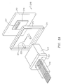
- an exemplary optical interconnect module 210 constructed in accordance with this invention has at least a base portion 212 and a lid portion 214 which forms the enclosure.
- the base 212 has optical-electrical (eg. an electro-optical transducer) 217 and electrical components 219 (eg. an integrated circuit) thereon for interfacing the optical signal carried by the optical cable 218 with an electronic signal.
- the base 212 may be integrally formed with the electrical components 219 and have optical-electrical components 219 mounted thereon.
- the optical electrical 217 and the electrical components 219 are operably coupled.
- the lid 214 can be affixed to the base portion 212, and is recessed to receive the optical-electrical 217 and electrical components 219.
- the lid 214 also has optical elements 224.
- the optical-electrical components 217 can be positioned between the electrical components 219 and the lid 214, and more particularly between the electrical components 219 and the optical elements 224.
- the optical cable 218 joins to the interconnect module 210 with a ferrule 217 that receives alignment members 222 in corresponding alignment receptacles 220.
- the lid 214 has alignment members 222 provided integrally thereon.
- Integral alignment members 222 need not be cylindrical pin shapes as discussed with reference to the prior art devices, but can be spherical, pyramid, cubic or virtually any shape and configuration that promotes alignment between the ferrule 217 and lid 214.
- the alignment receptacles 220 of the ferrule 217 have a corresponding shape to receive the alignment members and position the optical cable 218.
- the base 212 is fabricated primarily by mounting the optical-electrical 217 and electrical components 219 onto or into a base material. Then, the electrical connections required for interfacing the optical-electrical 217 and electrical components 219 with each other and with an electrical communications output (not shown) can be made.
- the electrical communications output is one of many devices known in the art which allows other electrical devices to interface with the interconnect module 210, for example an RJ-45 network cable jack or PC board interface.
- the bases 212 can be fabricated singularly, or multiple bases 212 can be fabricated on a unitary section of base material (FIG. 2C) and parted after some or all of the fabrication is complete.
- an exemplary lid 214 is constructed from a substrate material 228.
- the substrate material may be a ceramic such as glass, glass-ceramic, or quartz, or can be virtually any other optically transparent material that allows the optical signal to be transmitted there through. Alternately, only a portion of the substrate material need be transparent.
- the substrate 228 can be sized to build a single lid 214, or multiple lids 214 (FIG. 2C).
- the substrate 228 is sized to build multiple lids 214 allowing many of the processes described below to be performed as large batch processes. Performing the manufacturing processes as batch processes reduces the overall cost of the resultant device, because the processes can be performed repeatedly or simultaneously across a multiple lid substrate 228 minimizing the set-up time for each lid 214.
- Optical elements 224 such as focusing elements adapted to focus light into or out of the optical fibers of the optical cable 218, are formed into the substrate material 228 when the substrate 228 is molded.
- the optical elements 224 can be pre-fabricated and attached to the substrate material 228 during or after the construction of other features on the lid 214. Methods for forming the optical elements 224 into the substrate 228 or attaching pre-fabricated optical elements 224 to the substrate are known in the art and virtually any method of forming and attachment can be used.
- alignment fiducials 226 that aid in the placement of components, electrical, optical, optical-electrical, or otherwise, can be formed into or onto either surface of the lid 214.
- the lid 214 can be recessed to accept the optical-electrical 217 and electrical components 219 of the base by forming lip members 215 (FIG 2A) near its perimeter when the substrate 228 is molded.
- the lip members 215 can be machined into the substrate 228 or prefabricated lip members 215 affixed to the substrate during or after the construction of other features on the lid 214.
- the integral alignment members 222 can be formed by depositing a material onto the substrate 228.
- the material may be deposited in the desired shape for the integral alignment member 222.
- An exemplary material can be nickel deposited in a chemical vapor deposition (CVD) process, although one skilled in the art will appreciate that other metals and other materials in general can be combined with various deposition processes known in the art to achieve a similar result.
- a mold (not shown) can be used when depositing the material on the substrate 228 to ensure the precision and shape of the completed integral alignment member 222.
- the deposited material can be precision shaped after deposition, whether or not a mold is used.
- the deposited material may be precision shaped by physical machining, laser techniques or other acceptable precision shaping techniques. In some situations it is desirable to deposit a preliminary metal layer 232 on the surface of the substrate 228 to facilitate bonding of the deposited materials with the substrate 228.
- the integral alignment members 222 can also be formed from a curable or hardening material, such as a polymer resin or resin composite.
- the curable or hardening material bonds with the substrate 228 as it hardens.
- a mold (not shown) can be used to ensure the precision and shape of the completed integral alignment member 222.
- the cured or hardened material can also be shaped, whether or not a mold is used, by machining, laser techniques or other precision shaping techniques.
- the integral alignment members 222 can be pre-formed and affixed to the substrate 228.
- the integral alignment members 222 can be pre-formed from a ceramic, such as glass or quartz, a polymer, or a metal and then bonded to the substrate 228.
- Metallic integral alignment members 222 can also be affixed to the substrate 228 by providing a preliminary metal layer 232 and ultrasonically or thermally welding the metallic integral alignment members 222 into position.
- the preliminary metal layer 232 can be shaped to act as an alignment fiducial that aids in the positioning of the integral alignment member 222 on the substrate 228.
- each integral alignment member 222 can be provided with a larger cross-sectional area where the integral alignment member 222 meets the substrate 228.
- each integral alignment member 222 can have a flared base portion 233 at that the bonding or welding takes place.
- integral alignment members 222 can be pre-fabricated microspheres 236 set into recesses 238.
- the recesses ensure the desired positioning of the microspheres 234.
- the microspheres can be made of a ceramic such as glass, a polymer, or can be metal such as a ball bearing. Because microspheres are widely available commercially and generally manufactured in large quantities, this embodiment provides a very low cost source of pre-fabricated alignment members 222.
- the surface of the substrate 228 can be shaped to receive the base portions of pre-fabricated integral alignment members 222 or to receive for material to be deposited into in forming alignment member 222.
- the configuration can be designed to increase the contact area for bonding or welding in order to increase the strength of the attachment between the alignment member 222 and the substrate 228.
- the substrate surface can be shaped using photolithography techniques, wherein the substrate 228 is coated with photoresist, the photoresist exposed through a patterned mask, and the shapes etched (eg. deep-reactive-ion etching) through the resulting patterned photoresist. Using photolithography techniques can more precisely shape the substrate than mechanical processes.
- Recesses 240a, 240b can be of various configurations to promote precise positioning of the alignment members 222, whether formed from material built-up in the recesses or as pre-fabricated members. Additionaly, recesses 240a, 240b can have corresponding shapes to those on the integral alignment members 222, such as cylindrical (FIG. 5A), hemispherical or semi-hemispherical (FIG. 5B), or other shapes, such as pyramidal, octagonal, star-shaped, ovals or any other geometric configuration.
- FIG. 6 depicts an embodiment where the integral alignment members 222 are formed as part of the substrate material 228.
- the integral alignment members 222 are molded with the substrate 228 or the substrate material 228 can be removed, such as by machining, to shape the integral alignment members 222.
- the integral alignment members 222 can be etched from the substrate 228 or a deposited layer on the substrate 228 using photolithography techniques. For example, a photoresist is applied onto the substrate 228 and exposed in a pattern such that the substrate 228 can be etched to form alignment members 222 integrally thereon.
- an overlay 242 can be provided on which the integral alignment members 222 are bonded, welded, or formed as part of the overlay 242.
- the overlay 242 is affixed to the substrate 228, such as by bonding or welding to a preliminary metal layer on the substrate 228.
- the base 212, lid 214 and alignment members 222 can be constructed from a thermally stable glass having a low coefficient of thermal expansion.
- each base 212 and lid 214 pair can then be parted into their respective interconnect modules 210. If constructed in this manner, only one alignment step is required to align multiple lids 214 with their respective bases 212, whereas otherwise each lid 214 would have to be aligned individually with each base 212. Also, the base 212 and lid 214 pairs can be parted in a two step process whereby, the base material is cut with a thicker saw than the lid material. This results in each base 212 being slightly smaller than its lid 214, and the lid overlapping the base. The overlap provides convenient protection for electrical contacts that can be later formed on the lateral surfaces of the base 212.
Landscapes
- Physics & Mathematics (AREA)
- General Physics & Mathematics (AREA)
- Optics & Photonics (AREA)
- Optical Couplings Of Light Guides (AREA)
- Light Receiving Elements (AREA)
Abstract
Description
Claims (10)
- An enclosure for an optical communications device (210) that joins with a connector (221) of an optical cable (218), the enclosure comprising:a base portion (212);a lid portion (214) having focusing elements (224) and affixed to the base portion (212), wherein the lid portion (214) and the base portion (212) are adapted to receive at least a portion of the optical communications device (210) therebetween; andat least one alignment member (222) formed on the lid portion (214), the alignment member (222) adapted to interface with the connector (221) to align the connector (221) relative to lid portion (214).
- The enclosure of claim 1 wherein the at least one alignment member (222) is a prefabricated alignment member (222) bonded to the lid portion (214).
- The enclosure of claim 1 wherein the at least one alignment member (222) is shaped from the lid portion (214).
- The enclosure of claim 1 wherein the at least one alignment member (222) is a microsphere (236).
- The enclosure of any of claims 1 to 4 wherein the lid portion (214) further comprises at least one recess (238, 240) which receives the at least one alignment member (222).
- The enclosure of any of claims 1 to 5 wherein at least a portion of the lid portion (214) is transparent and at least one of the focusing elements (224) is formed into the lid portion (214).
- The enclosure of any of claims 1 to 6 wherein the at least one alignment member (222) is formed on an overlay (242), and the overlay (242) is affixed to the lid portion (214).
- A method of fabricating an optical interconnect device (210), the optical interconnect device (210) including optical-electrical components (217) for interfacing an optical and an electrical signal, comprising:forming at least two alignment members (222) on a substrate (214);affixing the substrate (214) to a base material (212) with at least a portion of the optical-electrical components (217) therebetween; andsegmenting the affixed substrate (214) and base (212) material into at least two portions of affixed substrate (214) and base (212) material, each portion having at least one alignment member (222).
- The method of claim 8 wherein forming the at least two alignment members (222) comprises etching the substrate (214) using photolithography techniques to form the at least two alignment members (222).
- The method of claim 8 wherein forming the at least two alignment members (222) comprises depositing material in the shape of the at least two alignment members (222).
Applications Claiming Priority (2)
| Application Number | Priority Date | Filing Date | Title |
|---|---|---|---|
| US10/007,494 US7128474B2 (en) | 2001-11-13 | 2001-11-13 | Optical device, enclosure and method of fabricating |
| US7494 | 2001-11-13 |
Publications (3)
| Publication Number | Publication Date |
|---|---|
| EP1310811A2 true EP1310811A2 (en) | 2003-05-14 |
| EP1310811A3 EP1310811A3 (en) | 2005-04-06 |
| EP1310811B1 EP1310811B1 (en) | 2007-02-21 |
Family
ID=21726518
Family Applications (1)
| Application Number | Title | Priority Date | Filing Date |
|---|---|---|---|
| EP02020396A Expired - Lifetime EP1310811B1 (en) | 2001-11-13 | 2002-09-12 | Optical device, enclosure and method of fabricating |
Country Status (3)
| Country | Link |
|---|---|
| US (1) | US7128474B2 (en) |
| EP (1) | EP1310811B1 (en) |
| DE (1) | DE60218266T2 (en) |
Cited By (2)
| Publication number | Priority date | Publication date | Assignee | Title |
|---|---|---|---|---|
| WO2006104950A1 (en) * | 2005-03-29 | 2006-10-05 | Intel Corporation | Passively aligned optical connection for opto-electronic array |
| US8079125B2 (en) | 2006-08-09 | 2011-12-20 | Hitachi, Ltd. | Manufacturing method of multi-channel optical module |
Families Citing this family (13)
| Publication number | Priority date | Publication date | Assignee | Title |
|---|---|---|---|---|
| US6757308B1 (en) * | 2002-05-22 | 2004-06-29 | Optical Communication Products, Inc. | Hermetically sealed transmitter optical subassembly |
| JP4548071B2 (en) * | 2004-09-29 | 2010-09-22 | ヤマハ株式会社 | Parts with guide pin insertion holes and their manufacturing methods |
| US20060245712A1 (en) * | 2005-04-29 | 2006-11-02 | Alexander Fishman | Devices, systems and methods for testing optoelectronic modules |
| CN101473258B (en) * | 2006-05-05 | 2014-11-19 | 里夫莱克斯光子公司 | Optically-enabled integrated circuit package |
| DE202007014173U1 (en) | 2007-10-10 | 2007-12-06 | CCS Technology, Inc., Wilmington | Coupling device for coupling at least one optical waveguide to an optical component |
| JP5195087B2 (en) * | 2008-06-30 | 2013-05-08 | 富士通株式会社 | Photoelectric conversion device, photoelectric conversion module, and method of manufacturing photoelectric conversion device |
| WO2013019189A1 (en) * | 2011-07-29 | 2013-02-07 | Hewlett-Packard Development Company, L.P. | Fiber optic connectors |
| TWI461775B (en) * | 2012-09-26 | 2014-11-21 | Delta Electronics Inc | Optical module and optical coupling method using the same |
| US9250404B2 (en) * | 2012-11-23 | 2016-02-02 | Electronics And Telecommunications Research Institute | Multi-channel optical module and manufacturing method of the same |
| US9134490B2 (en) * | 2012-12-06 | 2015-09-15 | Laxense Inc. | Passive alignment multichannel parallel optical system |
| US9170376B2 (en) * | 2012-12-14 | 2015-10-27 | Corning Cable Systems Llc | Optical port having a cover with a molded-in lens |
| US8992241B2 (en) * | 2013-04-30 | 2015-03-31 | International Business Machines Corporation | Flex circuit blind attachment apparatus and system |
| JP6506138B2 (en) * | 2015-08-18 | 2019-04-24 | 株式会社フジクラ | Optical module and receptacle for optical module |
Family Cites Families (17)
| Publication number | Priority date | Publication date | Assignee | Title |
|---|---|---|---|---|
| US5109453A (en) * | 1991-02-25 | 1992-04-28 | Amp Incorporated | Optical fiber connector with latching beam mechanism |
| US5138680A (en) * | 1991-04-17 | 1992-08-11 | Amp Incorporated | Optical fiber connector with elastomeric centering and floating alignment feature |
| US5450515A (en) * | 1993-04-29 | 1995-09-12 | Cts Corporation | Detachable fiber optic connector |
| EP0713111A1 (en) * | 1994-11-15 | 1996-05-22 | The Whitaker Corporation | Sealed multiposition fiber optic connector |
| US5590232A (en) * | 1995-02-16 | 1996-12-31 | Motorola, Inc. | Optical package and method of making |
| US5768456A (en) * | 1996-11-22 | 1998-06-16 | Motorola, Inc. | Optoelectronic package including photonic device mounted in flexible substrate |
| US6056448A (en) * | 1998-04-16 | 2000-05-02 | Lockheed Martin Corporation | Vertical cavity surface emitting laser array packaging |
| US6168317B1 (en) * | 1998-04-30 | 2001-01-02 | Lucent Technologies Inc. | Alignment adapter for an optical connector and method for making same |
| US6203212B1 (en) | 1998-08-24 | 2001-03-20 | Agilent Technologies, Inc. | Optical subassembly for use in fiber optic data transmission and reception |
| JP2000121889A (en) * | 1998-10-21 | 2000-04-28 | Nec Corp | Optical module and method for manufacturing the optical module |
| WO2000031771A1 (en) | 1998-11-25 | 2000-06-02 | Act Micro Devices | Optoelectronic module and method of making same |
| JP3824797B2 (en) | 1999-01-08 | 2006-09-20 | 古河電気工業株式会社 | Light emitting / receiving element module |
| US6318909B1 (en) | 1999-02-11 | 2001-11-20 | Agilent Technologies, Inc. | Integrated packaging system for optical communications devices that provides automatic alignment with optical fibers |
| US6137929A (en) | 1999-02-11 | 2000-10-24 | Agilent Technologies, Inc. | System and method for interfacing optical fibers with optical communications devices via an optical fiber faceplate |
| US6234687B1 (en) * | 1999-08-27 | 2001-05-22 | International Business Machines Corporation | Self-aligning method and interlocking assembly for attaching an optoelectronic device to a coupler |
| US6331079B1 (en) * | 1999-12-07 | 2001-12-18 | Molex Incorporated | Mounting system for a connector assembly to a substrate |
| US6450704B1 (en) * | 2000-10-05 | 2002-09-17 | Corona Optical Systems, Inc. | Transparent substrate and hinged optical assembly |
-
2001
- 2001-11-13 US US10/007,494 patent/US7128474B2/en not_active Expired - Lifetime
-
2002
- 2002-09-12 EP EP02020396A patent/EP1310811B1/en not_active Expired - Lifetime
- 2002-09-12 DE DE60218266T patent/DE60218266T2/en not_active Expired - Lifetime
Cited By (2)
| Publication number | Priority date | Publication date | Assignee | Title |
|---|---|---|---|---|
| WO2006104950A1 (en) * | 2005-03-29 | 2006-10-05 | Intel Corporation | Passively aligned optical connection for opto-electronic array |
| US8079125B2 (en) | 2006-08-09 | 2011-12-20 | Hitachi, Ltd. | Manufacturing method of multi-channel optical module |
Also Published As
| Publication number | Publication date |
|---|---|
| US7128474B2 (en) | 2006-10-31 |
| DE60218266T2 (en) | 2007-10-31 |
| EP1310811B1 (en) | 2007-02-21 |
| US20030091302A1 (en) | 2003-05-15 |
| DE60218266D1 (en) | 2007-04-05 |
| EP1310811A3 (en) | 2005-04-06 |
Similar Documents
| Publication | Publication Date | Title |
|---|---|---|
| US7128474B2 (en) | Optical device, enclosure and method of fabricating | |
| US10795086B2 (en) | Universal photonic adaptor for coupling an optical connector to an optoelectronic substrate | |
| JP4690963B2 (en) | Manufacturing method of multi-channel optical module | |
| US7362934B2 (en) | Optical connecting device and connector | |
| US20070206288A1 (en) | Hybrid optical/electronic structures fabricated by a common molding process | |
| US6250819B1 (en) | Mounting of an integrated optic circuit on a motherboard for the connection of optic fibers to form a miniature optical component | |
| US7369334B2 (en) | Optical device with alignment compensation | |
| EP4423552A1 (en) | Detachable connector for co-packaged optics | |
| US6181864B1 (en) | Optical fiber array module using soldering and fabrication method thereof | |
| US7223025B2 (en) | Packaging for a fiber-coupled optical device | |
| EP3798699B1 (en) | Fiber array spacers, optical assemblies incorporating fiber array spacers, and methods of fabricating the same | |
| JPH09510555A (en) | Photoelectric parts encapsulation | |
| JPH06337334A (en) | Optoelectronic transceiver submodule and manufacturing method thereof | |
| US5436996A (en) | Waferboard structure | |
| EP1312946B1 (en) | Method of manufacturing an optical mounting board | |
| US12345923B2 (en) | Metallized optical fiber array module and fabrication method thereof | |
| US5715338A (en) | Impermeable encapsulation of optoelectronic components | |
| US7010855B2 (en) | Optical module | |
| WO2002095464A1 (en) | Optical module and assembling method therefor | |
| US20030235388A1 (en) | Method for fabricating fiber blocks using solder as bonding material | |
| JP2005292379A (en) | Optical coupling device and manufacturing method thereof | |
| US5861637A (en) | Surface-mounted module which permits the light output of an optical semiconductor device mounted thereon to be increased, and a method of producing the surface-mounted module | |
| WO2003012496A2 (en) | Fabrication of an alignment microstructure in an optical assembly | |
| EP1367417A1 (en) | Optical fiber alignment technique | |
| JPS63311212A (en) | Optical waveguide device and optical waveguide mounting method |
Legal Events
| Date | Code | Title | Description |
|---|---|---|---|
| PUAI | Public reference made under article 153(3) epc to a published international application that has entered the european phase |
Free format text: ORIGINAL CODE: 0009012 |
|
| AK | Designated contracting states |
Designated state(s): AT BE BG CH CY CZ DE DK EE ES FI FR GB GR IE IT LI LU MC NL PT SE SK TR |
|
| AX | Request for extension of the european patent |
Extension state: AL LT LV MK RO SI |
|
| PUAL | Search report despatched |
Free format text: ORIGINAL CODE: 0009013 |
|
| AK | Designated contracting states |
Kind code of ref document: A3 Designated state(s): AT BE BG CH CY CZ DE DK EE ES FI FR GB GR IE IT LI LU MC NL PT SE SK TR |
|
| AX | Request for extension of the european patent |
Extension state: AL LT LV MK RO SI |
|
| 17P | Request for examination filed |
Effective date: 20050907 |
|
| AKX | Designation fees paid |
Designated state(s): DE GB |
|
| 17Q | First examination report despatched |
Effective date: 20060215 |
|
| GRAP | Despatch of communication of intention to grant a patent |
Free format text: ORIGINAL CODE: EPIDOSNIGR1 |
|
| RAP1 | Party data changed (applicant data changed or rights of an application transferred) |
Owner name: AVAGO TECHNOLOGIES FIBER IP (SINGAPORE) PTE. LTD. |
|
| GRAS | Grant fee paid |
Free format text: ORIGINAL CODE: EPIDOSNIGR3 |
|
| GRAA | (expected) grant |
Free format text: ORIGINAL CODE: 0009210 |
|
| AK | Designated contracting states |
Kind code of ref document: B1 Designated state(s): DE GB |
|
| REG | Reference to a national code |
Ref country code: GB Ref legal event code: FG4D |
|
| REF | Corresponds to: |
Ref document number: 60218266 Country of ref document: DE Date of ref document: 20070405 Kind code of ref document: P |
|
| PLBE | No opposition filed within time limit |
Free format text: ORIGINAL CODE: 0009261 |
|
| STAA | Information on the status of an ep patent application or granted ep patent |
Free format text: STATUS: NO OPPOSITION FILED WITHIN TIME LIMIT |
|
| 26N | No opposition filed |
Effective date: 20071122 |
|
| GBPC | Gb: european patent ceased through non-payment of renewal fee |
Effective date: 20070912 |
|
| PG25 | Lapsed in a contracting state [announced via postgrant information from national office to epo] |
Ref country code: GB Free format text: LAPSE BECAUSE OF NON-PAYMENT OF DUE FEES Effective date: 20070912 |
|
| REG | Reference to a national code |
Ref country code: DE Ref legal event code: R082 Ref document number: 60218266 Country of ref document: DE Representative=s name: DILG HAEUSLER SCHINDELMANN PATENTANWALTSGESELL, DE |
|
| REG | Reference to a national code |
Ref country code: DE Ref legal event code: R081 Ref document number: 60218266 Country of ref document: DE Owner name: AVAGO TECHNOLOGIES GENERAL IP (SINGAPORE) PTE., SG Free format text: FORMER OWNER: AVAGO TECHNOLOGIES FIBER IP (SINGAPORE) PTE. LTD., SINGAPORE, SG Effective date: 20130628 Ref country code: DE Ref legal event code: R082 Ref document number: 60218266 Country of ref document: DE Representative=s name: DILG HAEUSLER SCHINDELMANN PATENTANWALTSGESELL, DE Effective date: 20130628 |
|
| REG | Reference to a national code |
Ref country code: DE Ref legal event code: R082 Ref document number: 60218266 Country of ref document: DE Representative=s name: DILG, HAEUSLER, SCHINDELMANN PATENTANWALTSGESE, DE Ref country code: DE Ref legal event code: R081 Ref document number: 60218266 Country of ref document: DE Owner name: BROADCOM INTERNATIONAL PTE. LTD., SG Free format text: FORMER OWNER: AVAGO TECHNOLOGIES GENERAL IP (SINGAPORE) PTE. LTD., SINGAPORE, SG Ref country code: DE Ref legal event code: R082 Ref document number: 60218266 Country of ref document: DE Representative=s name: DILG HAEUSLER SCHINDELMANN PATENTANWALTSGESELL, DE Ref country code: DE Ref legal event code: R081 Ref document number: 60218266 Country of ref document: DE Owner name: AVAGO TECHNOLOGIES INTERNATIONAL SALES PTE. LT, SG Free format text: FORMER OWNER: AVAGO TECHNOLOGIES GENERAL IP (SINGAPORE) PTE. LTD., SINGAPORE, SG |
|
| PGFP | Annual fee paid to national office [announced via postgrant information from national office to epo] |
Ref country code: DE Payment date: 20190927 Year of fee payment: 18 |
|
| REG | Reference to a national code |
Ref country code: DE Ref legal event code: R082 Ref document number: 60218266 Country of ref document: DE Representative=s name: DILG, HAEUSLER, SCHINDELMANN PATENTANWALTSGESE, DE Ref country code: DE Ref legal event code: R081 Ref document number: 60218266 Country of ref document: DE Owner name: BROADCOM INTERNATIONAL PTE. LTD., SG Free format text: FORMER OWNER: AVAGO TECHNOLOGIES INTERNATIONAL SALES PTE. LTD., SINGAPUR, SG |
|
| REG | Reference to a national code |
Ref country code: DE Ref legal event code: R119 Ref document number: 60218266 Country of ref document: DE |
|
| PG25 | Lapsed in a contracting state [announced via postgrant information from national office to epo] |
Ref country code: DE Free format text: LAPSE BECAUSE OF NON-PAYMENT OF DUE FEES Effective date: 20210401 |