EP1309011A2 - Semiconductor component and method of operation - Google Patents
Semiconductor component and method of operation Download PDFInfo
- Publication number
- EP1309011A2 EP1309011A2 EP02024055A EP02024055A EP1309011A2 EP 1309011 A2 EP1309011 A2 EP 1309011A2 EP 02024055 A EP02024055 A EP 02024055A EP 02024055 A EP02024055 A EP 02024055A EP 1309011 A2 EP1309011 A2 EP 1309011A2
- Authority
- EP
- European Patent Office
- Prior art keywords
- doped region
- semiconductor substrate
- terminal
- semiconductor component
- transistor
- Prior art date
- Legal status (The legal status is an assumption and is not a legal conclusion. Google has not performed a legal analysis and makes no representation as to the accuracy of the status listed.)
- Withdrawn
Links
Images





Classifications
-
- H—ELECTRICITY
- H03—ELECTRONIC CIRCUITRY
- H03K—PULSE TECHNIQUE
- H03K17/00—Electronic switching or gating, i.e. not by contact-making and –breaking
- H03K17/08—Modifications for protecting switching circuit against overcurrent or overvoltage
-
- H—ELECTRICITY
- H10—SEMICONDUCTOR DEVICES; ELECTRIC SOLID-STATE DEVICES NOT OTHERWISE PROVIDED FOR
- H10D—INORGANIC ELECTRIC SEMICONDUCTOR DEVICES
- H10D30/00—Field-effect transistors [FET]
- H10D30/60—Insulated-gate field-effect transistors [IGFET]
- H10D30/601—Insulated-gate field-effect transistors [IGFET] having lightly-doped drain or source extensions, e.g. LDD IGFETs or DDD IGFETs
- H10D30/603—Insulated-gate field-effect transistors [IGFET] having lightly-doped drain or source extensions, e.g. LDD IGFETs or DDD IGFETs having asymmetry in the channel direction, e.g. lateral high-voltage MISFETs having drain offset region or extended drain IGFETs [EDMOS]
-
- H—ELECTRICITY
- H10—SEMICONDUCTOR DEVICES; ELECTRIC SOLID-STATE DEVICES NOT OTHERWISE PROVIDED FOR
- H10D—INORGANIC ELECTRIC SEMICONDUCTOR DEVICES
- H10D62/00—Semiconductor bodies, or regions thereof, of devices having potential barriers
- H10D62/10—Shapes, relative sizes or dispositions of the regions of the semiconductor bodies; Shapes of the semiconductor bodies
- H10D62/17—Semiconductor regions connected to electrodes not carrying current to be rectified, amplified or switched, e.g. channel regions
- H10D62/351—Substrate regions of field-effect devices
- H10D62/357—Substrate regions of field-effect devices of FETs
- H10D62/364—Substrate regions of field-effect devices of FETs of IGFETs
- H10D62/371—Inactive supplementary semiconductor regions, e.g. for preventing punch-through, improving capacity effect or leakage current
-
- H—ELECTRICITY
- H10—SEMICONDUCTOR DEVICES; ELECTRIC SOLID-STATE DEVICES NOT OTHERWISE PROVIDED FOR
- H10D—INORGANIC ELECTRIC SEMICONDUCTOR DEVICES
- H10D62/00—Semiconductor bodies, or regions thereof, of devices having potential barriers
- H10D62/10—Shapes, relative sizes or dispositions of the regions of the semiconductor bodies; Shapes of the semiconductor bodies
- H10D62/17—Semiconductor regions connected to electrodes not carrying current to be rectified, amplified or switched, e.g. channel regions
- H10D62/351—Substrate regions of field-effect devices
- H10D62/357—Substrate regions of field-effect devices of FETs
- H10D62/364—Substrate regions of field-effect devices of FETs of IGFETs
- H10D62/378—Contact regions to the substrate regions
-
- H—ELECTRICITY
- H10—SEMICONDUCTOR DEVICES; ELECTRIC SOLID-STATE DEVICES NOT OTHERWISE PROVIDED FOR
- H10D—INORGANIC ELECTRIC SEMICONDUCTOR DEVICES
- H10D8/00—Diodes
- H10D8/20—Breakdown diodes, e.g. avalanche diodes
- H10D8/25—Zener diodes
-
- H—ELECTRICITY
- H10—SEMICONDUCTOR DEVICES; ELECTRIC SOLID-STATE DEVICES NOT OTHERWISE PROVIDED FOR
- H10D—INORGANIC ELECTRIC SEMICONDUCTOR DEVICES
- H10D8/00—Diodes
- H10D8/411—PN diodes having planar bodies
-
- H—ELECTRICITY
- H10—SEMICONDUCTOR DEVICES; ELECTRIC SOLID-STATE DEVICES NOT OTHERWISE PROVIDED FOR
- H10D—INORGANIC ELECTRIC SEMICONDUCTOR DEVICES
- H10D84/00—Integrated devices formed in or on semiconductor substrates that comprise only semiconducting layers, e.g. on Si wafers or on GaAs-on-Si wafers
- H10D84/201—Integrated devices formed in or on semiconductor substrates that comprise only semiconducting layers, e.g. on Si wafers or on GaAs-on-Si wafers characterised by the integration of only components covered by H10D1/00 or H10D8/00, e.g. RLC circuits
- H10D84/204—Integrated devices formed in or on semiconductor substrates that comprise only semiconducting layers, e.g. on Si wafers or on GaAs-on-Si wafers characterised by the integration of only components covered by H10D1/00 or H10D8/00, e.g. RLC circuits of combinations of diodes or capacitors or resistors
-
- H—ELECTRICITY
- H10—SEMICONDUCTOR DEVICES; ELECTRIC SOLID-STATE DEVICES NOT OTHERWISE PROVIDED FOR
- H10D—INORGANIC ELECTRIC SEMICONDUCTOR DEVICES
- H10D84/00—Integrated devices formed in or on semiconductor substrates that comprise only semiconducting layers, e.g. on Si wafers or on GaAs-on-Si wafers
- H10D84/201—Integrated devices formed in or on semiconductor substrates that comprise only semiconducting layers, e.g. on Si wafers or on GaAs-on-Si wafers characterised by the integration of only components covered by H10D1/00 or H10D8/00, e.g. RLC circuits
- H10D84/204—Integrated devices formed in or on semiconductor substrates that comprise only semiconducting layers, e.g. on Si wafers or on GaAs-on-Si wafers characterised by the integration of only components covered by H10D1/00 or H10D8/00, e.g. RLC circuits of combinations of diodes or capacitors or resistors
- H10D84/221—Integrated devices formed in or on semiconductor substrates that comprise only semiconducting layers, e.g. on Si wafers or on GaAs-on-Si wafers characterised by the integration of only components covered by H10D1/00 or H10D8/00, e.g. RLC circuits of combinations of diodes or capacitors or resistors of only diodes
-
- H—ELECTRICITY
- H10—SEMICONDUCTOR DEVICES; ELECTRIC SOLID-STATE DEVICES NOT OTHERWISE PROVIDED FOR
- H10D—INORGANIC ELECTRIC SEMICONDUCTOR DEVICES
- H10D84/00—Integrated devices formed in or on semiconductor substrates that comprise only semiconducting layers, e.g. on Si wafers or on GaAs-on-Si wafers
- H10D84/40—Integrated devices formed in or on semiconductor substrates that comprise only semiconducting layers, e.g. on Si wafers or on GaAs-on-Si wafers characterised by the integration of at least one component covered by groups H10D12/00 or H10D30/00 with at least one component covered by groups H10D10/00 or H10D18/00, e.g. integration of IGFETs with BJTs
- H10D84/401—Combinations of FETs or IGBTs with BJTs
- H10D84/403—Combinations of FETs or IGBTs with BJTs and with one or more of diodes, resistors or capacitors
-
- H—ELECTRICITY
- H10—SEMICONDUCTOR DEVICES; ELECTRIC SOLID-STATE DEVICES NOT OTHERWISE PROVIDED FOR
- H10D—INORGANIC ELECTRIC SEMICONDUCTOR DEVICES
- H10D84/00—Integrated devices formed in or on semiconductor substrates that comprise only semiconducting layers, e.g. on Si wafers or on GaAs-on-Si wafers
- H10D84/60—Integrated devices formed in or on semiconductor substrates that comprise only semiconducting layers, e.g. on Si wafers or on GaAs-on-Si wafers characterised by the integration of at least one component covered by groups H10D10/00 or H10D18/00, e.g. integration of BJTs
- H10D84/611—Combinations of BJTs and one or more of diodes, resistors or capacitors
- H10D84/613—Combinations of vertical BJTs and one or more of diodes, resistors or capacitors
- H10D84/617—Combinations of vertical BJTs and only diodes
-
- H—ELECTRICITY
- H10—SEMICONDUCTOR DEVICES; ELECTRIC SOLID-STATE DEVICES NOT OTHERWISE PROVIDED FOR
- H10D—INORGANIC ELECTRIC SEMICONDUCTOR DEVICES
- H10D84/00—Integrated devices formed in or on semiconductor substrates that comprise only semiconducting layers, e.g. on Si wafers or on GaAs-on-Si wafers
- H10D84/80—Integrated devices formed in or on semiconductor substrates that comprise only semiconducting layers, e.g. on Si wafers or on GaAs-on-Si wafers characterised by the integration of at least one component covered by groups H10D12/00 or H10D30/00, e.g. integration of IGFETs
- H10D84/811—Combinations of field-effect devices and one or more diodes, capacitors or resistors
-
- H—ELECTRICITY
- H10—SEMICONDUCTOR DEVICES; ELECTRIC SOLID-STATE DEVICES NOT OTHERWISE PROVIDED FOR
- H10W—GENERIC PACKAGES, INTERCONNECTIONS, CONNECTORS OR OTHER CONSTRUCTIONAL DETAILS OF DEVICES COVERED BY CLASS H10
- H10W10/00—Isolation regions in semiconductor bodies between components of integrated devices
- H10W10/01—Manufacture or treatment
- H10W10/031—Manufacture or treatment of isolation regions comprising PN junctions
-
- H—ELECTRICITY
- H10—SEMICONDUCTOR DEVICES; ELECTRIC SOLID-STATE DEVICES NOT OTHERWISE PROVIDED FOR
- H10W—GENERIC PACKAGES, INTERCONNECTIONS, CONNECTORS OR OTHER CONSTRUCTIONAL DETAILS OF DEVICES COVERED BY CLASS H10
- H10W10/00—Isolation regions in semiconductor bodies between components of integrated devices
- H10W10/30—Isolation regions comprising PN junctions
Definitions
- This invention relates to electronics, in general, and to semiconductor components and methods of operation, in particular.
- semiconductor components are often used in automotive and other high voltage applications. These different types of semiconductor components include discrete devices and integrated circuits. As an example, the discrete devices can be power Metal-Oxide-Semiconductor (MOS) transistors having source, gate, and drain terminals. These different types of semiconductor components have been combined onto a single semiconductor chip to reduce the cost and space required for the semiconductor components.
- MOS Metal-Oxide-Semiconductor
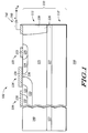
- FIG. 1 illustrates a partially schematic, cross-sectional view of a semiconductor component 100.
- semiconductor component 100 can be electrically coupled to a forty-volt power supply (not shown in FIG. 1).
- Semiconductor component 100 comprises a semiconductor substrate 110 having portions 111 and 112 with a first conductivity type.
- the first conductivity type can be a P-type conductivity.
- the first conductivity type can be an N-type conductivity.
- portion 111 can be an epitaxial portion having a preferred thickness of less than approximately four micrometers.
- portion 112 can be a substrate portion having a different doping concentration than portion 111.
- the semiconductor component also comprises a transistor 120 at least partially located in semiconductor substrate 110.
- Transistor 120 is a high power or high voltage transistor.
- transistor 120 can be a MOS transistor or a Bipolar Junction Transistor (BJT) capable of withstanding approximately forty to one hundred volts across its drain and source terminals or its collector and emitter terminals.
- BJT Bipolar Junction Transistor
- transistor 120 is a Laterally Diffused MOS (LDMOS) transistor.
- Transistor 120 is comprised of a doped region 121 in portion 111 of semiconductor substrate 110 and having the first conductivity type.
- doped region 121 can also be referred to as a well region for transistor 120.
- Transistor 120 also comprises a terminal 122 characterised by an electrode 123 and a doped region having a second conductivity type and located in portion 111 of semiconductor substrate 110 and over doped region 121.
- the second conductivity type can be an N-type conductivity.
- the first conductivity type is an N-type conductivity
- the second conductivity type can be a P-type conductivity.
- terminal 122 is a drain terminal for transistor 120.
- terminal 122 can be a collector terminal.
- the doped region of terminal 122 is comprised of doped regions 124 and 125.
- doped regions 124 and 125 can be referred to as a drift region and a drain region, respectively.
- doped region 125 has a higher doping concentration than doped regions 121 and 124.
- Transistor 120 additionally comprises a doped region 126 having the second conductivity type and located in semiconductor substrate 110 below portion 111 of semiconductor substrate 110 and above portion 112 of semiconductor substrate 110.
- doped region 126 can be located in a lower portion of portion 111 of semiconductor substrate 110 and an upper portion of portion 112 of semiconductor substrate 110.
- Doped region 126 is comprised of doped regions 127 and 128.
- Doped region 127 can be referred to as a buried layer or buried region.
- Doped region 126 separates portion 111 of semiconductor substrate 110 from portion 112 of semiconductor substrate 110.
- Doped region 126 can have a higher doping concentration than doped regions 121 and 124 and a lower doping concentration than doped region 125.
- Transistor 120 further comprises a terminal 129 characterised by an electrode 130 and a doped region 131 having the second conductivity type and located in portion 111 of semiconductor substrate 110 and over doped region 121.
- terminal 129 can be referred to as a source terminal.
- terminal 129 can be referred to as an emitter terminal.
- Transistor 120 still further comprises doped regions 132 and 133 having the first conductivity type.
- Doped region 133 can be referred to as a body region.
- doped region 132 can have a higher doping concentration than doped regions 121, 126, and 133.
- Transistor 120 also comprises a terminal 134 characterised by an electrode 135 and an electrically insulative layer 136, both located over a top surface of semiconductor substrate 110.
- terminal 134 can be referred to as a gate terminal.
- terminal 134 can be referred to as a base terminal.
- transistor 120 additionally comprises an intrinsic BJT formed at least partially from doped regions 121, 125, and 126.
- doped region 121 when terminal 122 is forward biased with respect to doped region 121, doped region 121 can be the base region of the intrinsic BJT; doped region 125 can be the emitter of the intrinsic BJT; and doped region 126 can be the collector of the intrinsic BJT.
- doped region 121 when terminal 122 is reverse biased with respect to doped region 121, doped region 121 can be the base region of the intrinsic BJT; doped region 125 can be the collector of the intrinsic BJT; and doped region 126 can be the emitter of the intrinsic BJT.
- the intrinsic BJT is active or turned-on when terminal 122 is forward biased relative to doped region 121, and the intrinsic bipolar junction transistor is deactivated or turned-off when terminal 122 is reverse biased relative to doped region 121.
- the activation and deactivation of the intrinsic BJT are explained in more detail hereinafter.
- semiconductor component 100 further comprises an integrated circuit 140 at least partially located in semiconductor substrate 110 and electrically coupled to transistor 120. Doped region 126 separates or isolates transistor 120 from integrated circuit 140.
- Semiconductor component 100 still further comprises a switching circuit 150 electrically coupled to doped region 126 to adjust the bias of doped region 126.
- Switching circuit 150 is illustrated in schematic form in FIG. 1. In a first embodiment, switching circuit 150 is at least partially located in semiconductor substrate 110. In a second embodiment, switching circuit 150 is at least partially located over semiconductor substrate 110. In a third embodiment, switching circuit 150 is entirely located outside of semiconductor substrate 110.
- Switching circuit 150 biases doped region 126 to prevent substrate injection when doped region 125 is forward biased with respect to doped region 121 and to prevent punchthrough when doped region 125 is reverse-biased with respect to doped region 121.
- the use of switching circuit 150 eliminates the need for more costly and more complicated epitaxial layers having higher doping concentrations towards doped region 127 to prevent punch-through between the doped region 125 and doped region 126.
- the use of switching circuit 150 also eliminates the need for thicker epitaxial layers, which are incompatible with industry goals for thinner epitaxial layers, especially for fiber optic applications.
- Switching circuit 150 also biases doped region 126 to activate and deactivate the intrinsic BJT in transistor 120.
- the biasing provided by switching circuit 150 is dynamically performed during the operation of transistor 120.
- switching circuit 150 biases doped region 126 in a direction identical to a biasing direction of terminal 122 when terminal 122 is reverse biased relative to doped region 121. In the preferred embodiment, such biasing of doped region 126 and terminal 122 occurs substantially simultaneously. This biasing deactivates or turns off the intrinsic BJT in transistor 120.
- switching circuit 150 biases doped region 126 at zero volts or reverse bias relative to portion 112 of semiconductor substrate 110 when terminal 122 is forward biased relative to doped region 121. In the preferred embodiment, such biasing of doped region 126 and terminal 122 occurs substantially simultaneously. This biasing deactivates or turns off the intrinsic BJT in transistor 120.
- switching circuit 150 comprises a single diode 160.
- diode 160 is a P-N diode and is electrically coupled to buried region 126.
- Diode 160 can be at least partially located in semiconductor substrate 110.
- buried region 126 can be electrically floating.
- terminal 122 When terminal 122 is forward biased with respect to doped region 121, the voltage of doped region 126 equals Vin, and the BJT is activated. When terminal 122 is reverse biased with respect to doped region 121 and is larger than Vin, the voltage of doped region 126 equals the voltage at terminal 122, and the intrinsic BJT is deactivated.
- FIG. 2 illustrates a cross-sectional view of a semiconductor component 200, which is an embodiment of semiconductor component 100 in FIG. 1.
- Diode 160 in semiconductor component 200 in FIG. 2 comprises a doped region 261 in portion 111 of semiconductor substrate 110, a doped region 262 in portion 111 of semiconductor substrate 110, a portion of portion 111 of semiconductor substrate 110, and doped region 126.
- Doped regions 261 and 262 have the first conductivity type, and doped region 261 has a higher doping concentration than doped region 262 and the portion of portion 111 of semiconductor substrate 110.
- Diode 160 can be added to semiconductor component 200 without requiring any additional manufacturing steps.
- doped region 261 can be formed simultaneously with doped region 132
- doped region 262 can be formed simultaneously with doped region 133.
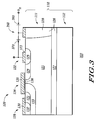
- FIG. 3 illustrates a partially schematic, cross-sectional view of a semiconductor component 300, which can be a different embodiment of semiconductor component 100 in FIG. 1. Similar to semiconductor component 100 in FIG. 1, semiconductor component 300 in FIG. 3 comprises transistor 120 and integrated circuit 140. For simplicity, integrated circuit 140 in FIG. 1 is not illustrated in FIG. 3.
- Switching circuit 350 comprises diodes 360 and 370.
- diodes 360 and 370 are P-N diodes electrically coupled to each other.
- diodes 360 and 370 can be configured in a back-to-back arrangement where diode 370 electrically couples together doped region 125 and doped region 126 and where diode 360 electrically couples together doped region 126 and an input voltage (Vin).
- Diodes 360 and 370 can be at least partially located in semiconductor substrate 110.
- diode 370 In operation, when the voltage applied to terminal 122 is greater than the input voltage, diode 370 is turned on, and diode 360 is turned off. Under these conditions, doped region 126 is approximately electrically shorted or otherwise electrically coupled to terminal 122. Also under these conditions, transistor 120 has a high drain-to-source breakdown voltage. When the voltage applied to terminal 122 is less than the input voltage, diode 370 is turned off, and diode 360 is turned on. Under these conditions, doped region 126 is not electrically shorted to terminal 122.
- the input voltage can be offset from the voltage applied to terminal 122 by approximately fifteen volts or less.
- diode 370 is preferably a high voltage diode, and diode 360 can be a low voltage diode.
- the input voltage is approximately one to five volts.
- FIG. 4 illustrates a cross-sectional view of a semiconductor component 400, which is an embodiment of semiconductor component 300 in FIG. 3.
- Diode 360 in semiconductor component 400 in FIG. 4 comprises a doped region 461 in portion 111 of semiconductor substrate 110, a doped region 462 in portion 111 of semiconductor substrate 110, a portion of portion 111 of semiconductor substrate 110, and doped region 126.
- Doped regions 461 and 462 have the first conductivity type, and doped region 461 has a higher doping concentration than doped region 462 and the portion of portion 111 of semiconductor substrate 110.
- Diode 370 in semiconductor component 400 comprises a doped region 471 and doped region 126.
- Doped region 471 has the first conductivity type.
- doped region 462 is separated from doped region 128 by approximately two to five microns.
- Diodes 360 and 370 can be added to semiconductor component 400 without requiring any additional manufacturing steps.
- doped regions 461 and 471 can be formed simultaneously with doped region 132
- doped region 462 can be formed simultaneously with doped region 133.
- Empirical results for a semiconductor component, such as semiconductor component 400, have demonstrated that the back-to-back diode scheme of diodes 360 and 370 is fast enough to switch simultaneously with transistor 120 to prevent premature breakdown within transistor 120.
- FIG. 5 illustrates a cross-sectional view of a semiconductor component 500, which is an embodiment of semiconductor component of FIG. 3.
- semiconductor component 500 in FIG. 5 comprises a diode 570 that is at least partially formed in semiconductor substrate 110.
- Diode 570 comprises doped regions 521, 571, 572, 573, and 574.
- Doped regions 521, 571, and 572 have the first conductivity type, and doped regions 573 and 574 have the second conductivity type.
- Doped regions 571 and 572 have higher doping concentrations than doped region 521, and doped region 573 has a higher doping concentration than doped region 574.
- Diode 570 is formed from a BJT having its emitter terminal electrically coupled to doped region 125 and having its base and collector terminals electrically coupled to each other and to doped region 128.
- the electrical coupling together of the base and collector terminals to doped region 128 is facilitated by a doped region 575 of the second conductivity type.
- the collector terminal for the BJT comprises doped regions 571 and 521; the base terminal for the BJT comprises doped regions 573 and 574; and the emitter terminal for the BJT comprises doped region 572.
- Diode 570 also comprises doped regions 127, 128, and 528, which electrically isolate diode 570 from transistor 120.
- Diode 370 in FIG. 3 is not electrically isolated from transistor 120 in semiconductor component 300. Therefore, under certain conditions, diode 370 may inject undesirable minority carriers into transistor 120. This problem of diode 370 in FIG. 3 is eliminated by diode 570 in FIG. 5.
- doped region 126 can comprise doped regions 127, 128, and 528.
- Diode 570 can be added to semiconductor component 500 without requiring any additional manufacturing steps.
- doped regions 571 and 572 can be formed simultaneously with doped regions 132 and 461, and doped regions 573 and 575 can be formed simultaneously with doped regions 125 and 131.
- doped region 574 can be formed simultaneously with other base regions of other BJTs in the integrated circuit of semiconductor component 500, and doped region 521 can be formed simultaneously with doped region 121.
- doped region 528 can be formed simultaneously with doped region 128.
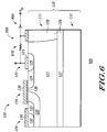
- FIG. 6 illustrates a partially schematic, cross-sectional view of a semiconductor component 600, which can be a different embodiment of semiconductor component 100 in FIG. 1. Similar to semiconductor component 100 in FIG. 1, semiconductor component 600 in FIG. 6 comprises transistor 120 and integrated circuit 140. For simplicity, integrated circuit 140 in FIG. 1 is not illustrated in FIG. 6.
- Switching circuit 650 comprises a diode 660 and a resistor 670. As illustrated in FIG. 6, diode 660 and resistor 670 are electrically coupled to each other. As an example, diode 660 and resistor 670 can be configured such that resistor 670 electrically couples together terminal 122 and doped region 126 and where diode 660 electrically couples together doped region 126 and an input voltage (Vin). Diode 660 and resistor 670 can be at least partially located in semiconductor substrate 110.
- the input voltage can be offset from the voltage applied to terminal 122 by approximately fifteen volts or less.
- resistor 670 preferably has a high resistance
- diode 660 can be a low voltage diode.
- the input voltage is approximately one to five volts.
- FIG. 7 illustrates a cross-sectional view of a semiconductor component 700, which is an embodiment of semiconductor component 600 of FIG. 6.
- Diode 660 in semiconductor component 700 in FIG. 7 comprises a doped region 761 in portion 111 of semiconductor substrate 110, a doped region 762 in portion 111 of semiconductor substrate 110, a portion of portion 111 of semiconductor substrate 110, and doped region 126.
- Doped regions 761 and 762 have the first conductivity type, and doped region 761 has a higher doping concentration than doped region 762 and the portion of portion 111 of semiconductor substrate 110.
- doped region 762 is separated from doped region 128 by approximately two to five microns.
- Semiconductor component 700 also comprises a doped region 771 having the second conductivity type to facilitate the electrical coupling between doped region 126 and resistor 670.
- Resistor 670 in semiconductor component 700 is preferably formed over the top surface of semiconductor substrate 110.
- Resistor 670 is also preferably comprised of polycrystalline silicon. In a different embodiment, resistor 670 can be formed at least partially within semiconductor substrate 110.
- Diode 660 can be added to semiconductor component 700 without requiring any additional manufacturing steps.
- doped region 761 can be formed simultaneously with doped region 132
- doped region 762 can be formed simultaneously with doped region 133
- doped region 771 can be formed simultaneously with doped regions 125 and 131.
- FIG. 8 illustrates a partially schematic, cross-sectional view of a semiconductor component 800, which can be a different embodiment of semiconductor component 100 in FIG. 1. Similar to semiconductor component 100 in FIG. 1, semiconductor component 800 in FIG. 8 comprises transistor 120 and integrated circuit 140. For simplicity, integrated circuit 140 in FIG. 1 is not illustrated in FIG. 8.
- Switching circuit 850 comprises a diode 860, a resistor 870, and a transistor 880. As illustrated in FIG. 8, diode 860, resistor 870, and transistor 880 are electrically coupled to each other. Diode 860, resistor 870, and transistor 880 can be at least partially located in semiconductor substrate 110.
- transistor 880 can be a BJT having an emitter terminal, a base terminal, and a collector terminal. Transistor 880 is electrically coupled to doped region 126. As illustrated in FIG. 8, the emitter terminal of transistor 880 is electrically coupled to doped region 128 of doped region 126.
- diode 860 can be a Zener diode.
- Diode 860 electrically couples terminal 122 to transistor 880 and resistor 870. As illustrated in FIG. 8, diode 860 electrically couples doped region 125 to the base terminal of transistor 880.
- resistor 870 can be a polycrystalline silicon resistor and can have a high resistance. Resistor 870 electrically couples the collector terminal of transistor 880 to diode 860 and the base terminal of transistor 880.
- the voltage of doped region 126 equals the voltage of terminal 122 plus a voltage drop across the reverse-biased Zener diode minus a voltage drop across the base to emitter of the transistor. For example, if the base-to-emitter voltage equals approximately 0.7 volts and the drop across diode 860 equals approximately 5 volts, then the voltage of doped region 126 is approximately 4.3 volts higher than voltage of terminal 122. Hence, when terminal 122 is forward biased with respect to doped region 121, then the injected current from doped region 125 is collected by doped region 126. Also, when terminal 122 is reverse biased with respect to doped region 121, then the offset voltage between doped region 126 and terminal 122 causes the BJT to be deactivated or turned-off.
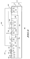
- FIG. 9 illustrates a cross-sectional view of a semiconductor component 900, which is an embodiment of semiconductor component 800 of FIG. 8.
- Transistor 880 in semiconductor component 900 comprises doped regions 981, 982, 983, 984, 985, 986, 987, and 988.
- Doped regions 981 and 982 have the first conductivity type
- doped regions 983, 984, 985, 986, 987, and 988 have the second conductivity type.
- Doped region 981 has a higher doping concentration than doped region 982, and doped regions 983 and 985 have higher doping concentrations than doped regions 984, 986, 987, and 988.
- Doped regions 986, 987, and 988 have higher doping concentrations than doped region 984.
- transistor 880 is a BJT with emitter, collector, and base terminals.
- the collector terminal for the BJT comprises doped regions 984, 985, 986, 987, and 988;
- the base terminal for the BJT comprises doped regions 981 and 982; and
- the emitter terminal for the BJT comprises doped region 983.
- the emitter terminal of transistor 880 is electrically coupled to doped region 128, and this electrical coupling is facilitated by a doped region 989 of the second conductivity type.
- Doped regions 986, 988, and 987 electrically isolate transistor 880 from transistor 120.
- Diode 860 comprises doped regions 961, 962, and 963.
- Doped regions 961 and 962 have the second conductivity type, and doped region 963 has the first conductivity type.
- Doped region 961 has a higher doping concentration than doped region 962.
- Diode 860 and transistor 880 can be added to semiconductor component 800 without requiring any additional manufacturing steps.
- doped regions 961, 983, 985, and 989 can be formed simultaneously with doped regions 125 and 131, and doped regions 963 and 981 can be formed simultaneously with doped region 132.
- doped regions 962, 986, and 987 can be formed simultaneously with doped region 128, and doped region 988 can be formed simultaneously with doped region 127.
- doped regions 982 and 984 can be formed simultaneously with other base and collector regions of other BJTs in the integrated circuit of semiconductor component 900.
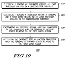
- FIG. 10 illustrates a flow chart 1000 of a method of operating a semiconductor component.
- the semiconductor component of flow chart 1000 can be similar to semiconductor components 100, 200, 300, 400, 500, 600, 700, 800, and/or 900 in FIGs. 1, 2, 3, 4, 5, 6, 7, 8, and 9, respectively.
- an integrated circuit at least partially located in a semiconductor substrate is electrically biased.
- the integrated circuit can be similar to integrated circuit 140 in FIG. 1.
- a transistor at least partially located in the semiconductor substrate is electrically biased.
- the transistor can be similar to transistor 120 in FIGs. 1, 2, 3, 4, 5, 6, 7, 8, and 9.
- a first doped region in a first portion of the semiconductor substrate and having a first conductivity type can comprise (1) a first doped region in a first portion of the semiconductor substrate and having a first conductivity type, (2) a terminal characterised by a second doped region having a second conductivity type and located in the first portion of the semiconductor substrate and over the first doped region, (3) a third doped region having the second conductivity type, located in the semiconductor substrate below the first portion of the semiconductor substrate and above a second portion of the semiconductor substrate having the first conductivity type, and separating the first portion of the semiconductor substrate from the second portion of the semiconductor substrate, and (4) an intrinsic bipolar junction transistor formed at least partially from the first, second, and third doped regions.
- the intrinsic bipolar junction transistor is deactivated when the drain terminal is reverse biased relative to the first doped region.
- the third doped region can be electrically biased to deactivate the intrinsic bipolar junction transistor.
- the third doped region can be electrically biased in a direction identical to a biasing direction of the terminal when the terminal is reverse biased relative to the first doped region.
- Step 1030 of flow chart 1000 prevents or otherwise suppresses the generation and injection of minority carriers into a substrate portion or the second portion of the semiconductor substrate.
- the intrinsic bipolar junction transistor is activated when the drain terminal is forward biased relative to the first doped region.
- the third doped region can be electrically biased to activate the intrinsic bipolar junction transistor.
- the third doped region can be electrically biased at zero volts or reverse bias relative to the second portion of the semiconductor substrate when the terminal is forward biased relative to the first doped region.
- Step 1040 of flow chart 1000 enables the transistor of step 1020 to have a high drain-to-source breakdown voltage.
- steps 1020 and 1030 of flow chart 1000 prevent punch-through between the second doped region and the third doped region of the transistor.
- steps 1030 can be performed before step 1020.
- steps 1010, 1020, and 1030 can be performed simultaneously with each other; and steps 1010, 1020, and 1040 can be performed simultaneously with each other.
- the semiconductor component has a power transistor combined with an integrated circuit onto a single semiconductor substrate where the power transistor has a high drain-to-source breakdown voltage and is electrically isolated from the integrated circuit.
- the semiconductor substrate can comprise a thin epitaxial semiconductor layer, in which the power transistor and the integrated circuit are formed.
- a method of operating a semiconductor component also suppresses the injection of minority carriers into the semiconductor substrate.
- the invention has been described with reference to specific embodiments, it will be understood by those skilled in the art that various changes may be made without departing from the spirit or scope of the invention.
- the numerous details set forth herein such as, for example, the dimensions, the relative doping concentrations, and the specific diodes, resistors, and transistors used in the switching circuits are provided to facilitate the understanding of the invention and are not provided to limit the scope of the invention.
- the diodes in the switching circuits can be Schottky diodes
- the resistors in the switching circuits can be crystalline silicon diodes formed in the semiconductor substrate. Accordingly, the disclosure of embodiments of the invention is intended to be illustrative of the scope of the invention and is not intended to be limiting. It is intended that the scope of the invention shall be limited only to the extent required by the appended claims.
Landscapes
- Metal-Oxide And Bipolar Metal-Oxide Semiconductor Integrated Circuits (AREA)
- Bipolar Integrated Circuits (AREA)
- Bipolar Transistors (AREA)
- Junction Field-Effect Transistors (AREA)
Abstract
Description
Claims (9)
- A semiconductor component characterized by:wherein:a semiconductor substrate having first and second portions with a first conductivity type;a transistor at least partially located in the semiconductor substrate and characterised by:a first doped region in the first portion of the semiconductor substrate and having the first conductivity type;a terminal characterised by a second doped region having a second conductivity type and located in the first portion of the semiconductor substrate and over the first doped region; anda third doped region having the second conductivity type and located in the semiconductor substrate below the first portion of the semiconductor substrate and above the second portion of the semiconductor substrate;a fourth doped region having the first conductivity type formed within the first doped region and electrically coupled to the first doped region; anda terminal electrically coupled to the fourth doped region for providing a bias to the fourth doped region and the first doped region; anda switching circuit electrically coupled to the third doped region to adjust a bias of the third doped region,the third doped region separates the first portion of the semiconductor substrate from the second portion of the semiconductor substrate.
- The semiconductor component of claim 1 wherein:the switching circuit biases the third doped region to prevent punch-through between the second and third doped regions.
- The semiconductor component of claim 1 wherein:the switching circuit biases the third doped region in a direction identical to a biasing direction of the terminal when the terminal is reverse biased relative to the first doped region.
- The semiconductor component of claim 1 wherein:the switching circuit biases the third doped region at zero volts or reverse bias relative to the second portion of the semiconductor substrate when the terminal is forward biased relative to the first doped region.
- The semiconductor component of claim 1 wherein:the transistor further comprises:an intrinsic bipolar junction transistor formed at least partially from the first, second, and third doped regions;the intrinsic bipolar junction transistor is active when the terminal is forward biased relative to the first doped region; andthe switching circuit deactivates the intrinsic bipolar junction transistor when the terminal is reverse biased relative to the first doped region.
- The semiconductor component of claim 1 wherein:the switching circuit comprises a single diode.
- The semiconductor component of claim 1 wherein:the switching circuit comprises two diodes.
- The semiconductor component of claim 1 wherein:the switching circuit comprises:a bipolar junction transistor;a diode; anda resistor.
- The semiconductor component of claim 1 wherein:the switching circuit comprises:a resistor; anda diode.
Applications Claiming Priority (2)
| Application Number | Priority Date | Filing Date | Title |
|---|---|---|---|
| US4186 | 2001-10-31 | ||
| US10/004,186 US6573562B2 (en) | 2001-10-31 | 2001-10-31 | Semiconductor component and method of operation |
Publications (2)
| Publication Number | Publication Date |
|---|---|
| EP1309011A2 true EP1309011A2 (en) | 2003-05-07 |
| EP1309011A3 EP1309011A3 (en) | 2008-07-02 |
Family
ID=21709583
Family Applications (1)
| Application Number | Title | Priority Date | Filing Date |
|---|---|---|---|
| EP02024055A Withdrawn EP1309011A3 (en) | 2001-10-31 | 2002-10-28 | Semiconductor component and method of operation |
Country Status (2)
| Country | Link |
|---|---|
| US (1) | US6573562B2 (en) |
| EP (1) | EP1309011A3 (en) |
Cited By (4)
| Publication number | Priority date | Publication date | Assignee | Title |
|---|---|---|---|---|
| WO2004042826A3 (en) * | 2002-10-31 | 2004-07-29 | Motorola Inc | Semiconductor component comprising a resur transistor and method of manufacturing same |
| WO2006132704A3 (en) * | 2005-06-02 | 2007-04-05 | Freescale Semiconductor Inc | High voltage igbt semiconductor device and method of manufacture |
| WO2011126609A2 (en) | 2010-03-30 | 2011-10-13 | Freescale Semiconductor, Inc. | Semiconductor device and method |
| EP1966826A4 (en) * | 2005-10-31 | 2013-06-19 | Freescale Semiconductor Inc | SEMICONDUCTOR DEVICE AND METHOD OF FORMING THE SAME |
Families Citing this family (23)
| Publication number | Priority date | Publication date | Assignee | Title |
|---|---|---|---|---|
| US7141860B2 (en) * | 2004-06-23 | 2006-11-28 | Freescale Semiconductor, Inc. | LDMOS transistor |
| US7187033B2 (en) * | 2004-07-14 | 2007-03-06 | Texas Instruments Incorporated | Drain-extended MOS transistors with diode clamp and methods for making the same |
| US7608907B2 (en) * | 2005-01-06 | 2009-10-27 | Micrel, Inc. | LDMOS gate controlled schottky diode |
| US7297603B2 (en) * | 2005-03-31 | 2007-11-20 | Semiconductor Components Industries, L.L.C. | Bi-directional transistor and method therefor |
| US7439584B2 (en) * | 2005-05-19 | 2008-10-21 | Freescale Semiconductor, Inc. | Structure and method for RESURF LDMOSFET with a current diverter |
| US7466006B2 (en) * | 2005-05-19 | 2008-12-16 | Freescale Semiconductor, Inc. | Structure and method for RESURF diodes with a current diverter |
| JP4955222B2 (en) | 2005-05-20 | 2012-06-20 | ルネサスエレクトロニクス株式会社 | Manufacturing method of semiconductor device |
| US7180158B2 (en) * | 2005-06-02 | 2007-02-20 | Freescale Semiconductor, Inc. | Semiconductor device and method of manufacture |
| KR100770539B1 (en) * | 2006-08-11 | 2007-10-25 | 동부일렉트로닉스 주식회사 | Semiconductor device and manufacturing method thereof |
| KR20100079705A (en) * | 2008-12-31 | 2010-07-08 | 주식회사 동부하이텍 | Lateral double diffused metal oxide semiconductor device |
| US10418809B2 (en) * | 2012-04-23 | 2019-09-17 | Active-Semi, Inc. | Power management integrated circuit for driving inductive loads |
| US9142554B2 (en) * | 2012-06-29 | 2015-09-22 | Freescale Semiconductor, Inc. | Semiconductor device and driver circuit with an active device and isolation structure interconnected through a diode circuit, and method of manufacture thereof |
| US9111767B2 (en) | 2012-06-29 | 2015-08-18 | Freescale Semiconductor, Inc. | Semiconductor device and driver circuit with source and isolation structure interconnected through a diode circuit, and method of manufacture thereof |
| US9129990B2 (en) * | 2012-06-29 | 2015-09-08 | Freescale Semiconductor, Inc. | Semiconductor device and driver circuit with drain and isolation structure interconnected through a diode circuit, and method of manufacture thereof |
| US20140001546A1 (en) * | 2012-06-29 | 2014-01-02 | Hubert M. Bode | Semiconductor device and driver circuit with a current carrying region and isolation structure interconnected through a resistor circuit, and method of manufacture thereof |
| US8673712B2 (en) * | 2012-07-20 | 2014-03-18 | Taiwan Semiconductor Manufacturing Company, Ltd. | Power transistor with high voltage counter implant |
| JP6156841B2 (en) * | 2012-11-07 | 2017-07-05 | エヌエックスピー ユーエスエイ インコーポレイテッドNXP USA,Inc. | SEMICONDUCTOR DEVICE AND DRIVER CIRCUIT HAVING ACTIVE DEVICE AND ISOLATED STRUCTURE INTERCONNECTED THROUGH RESISTANCE CIRCUIT AND ITS MANUFACTURING METHOD |
| JP6222825B2 (en) * | 2012-11-07 | 2017-11-01 | エヌエックスピー ユーエスエイ インコーポレイテッドNXP USA,Inc. | SEMICONDUCTOR DEVICE AND DRIVER CIRCUIT HAVING ACTIVE ELEMENT AND ISOLATED STRUCTURE INTERCONNECTED THROUGH DIODE CIRCUIT AND METHOD FOR MANUFACTURING THE SAME |
| US9702925B2 (en) * | 2014-10-15 | 2017-07-11 | Nxp Usa, Inc. | Semiconductor device with upset event detection and method of making |
| US9666710B2 (en) * | 2015-05-19 | 2017-05-30 | Nxp Usa, Inc. | Semiconductor devices with vertical field floating rings and methods of fabrication thereof |
| US9741849B1 (en) * | 2016-04-08 | 2017-08-22 | Globalfoundries Singapore Pte. Ltd. | Integrated circuits resistant to electrostatic discharge and methods for producing the same |
| US20200194581A1 (en) * | 2018-12-18 | 2020-06-18 | Vanguard International Semiconductor Corporation | Semiconductor device and method for forming the same |
| US20240047569A1 (en) * | 2022-08-08 | 2024-02-08 | Leap Semiconductor Corp. | Silicon carbide semiconductor power transistor and method of manufacturing the same |
Family Cites Families (6)
| Publication number | Priority date | Publication date | Assignee | Title |
|---|---|---|---|---|
| FR2655196B1 (en) * | 1989-11-29 | 1992-04-10 | Sgs Thomson Microelectronics | DYNAMIC ISOLATION CIRCUIT OF INTEGRATED CIRCUITS. |
| EP0520125B1 (en) * | 1991-06-27 | 1997-08-20 | Consorzio per la Ricerca sulla Microelettronica nel Mezzogiorno - CoRiMMe | Switching circuit for connecting a first circuit node to a second or to a third circuit node according to the latter's potential, for controlling the potential of an insulation region of an integrated circuit according to the substrate's potential |
| IT1252623B (en) * | 1991-12-05 | 1995-06-19 | Sgs Thomson Microelectronics | SEMICONDUCTOR DEVICE INCLUDING AT LEAST A POWER TRANSISTOR AND AT LEAST A CONTROL CIRCUIT, WITH DYNAMIC INSULATION CIRCUIT, INTEGRATED IN A MONOLITHIC MANNER IN THE SAME PLATE |
| EP0734070B1 (en) * | 1995-03-22 | 2000-07-19 | Consorzio per la Ricerca sulla Microelettronica nel Mezzogiorno - CoRiMMe | Method and device for dynamically self-biasing regions of integrated circuits |
| TW417307B (en) * | 1998-09-23 | 2001-01-01 | Koninkl Philips Electronics Nv | Semiconductor device |
| US6413806B1 (en) * | 2000-02-23 | 2002-07-02 | Motorola, Inc. | Semiconductor device and method for protecting such device from a reversed drain voltage |
-
2001
- 2001-10-31 US US10/004,186 patent/US6573562B2/en not_active Expired - Lifetime
-
2002
- 2002-10-28 EP EP02024055A patent/EP1309011A3/en not_active Withdrawn
Cited By (6)
| Publication number | Priority date | Publication date | Assignee | Title |
|---|---|---|---|---|
| WO2004042826A3 (en) * | 2002-10-31 | 2004-07-29 | Motorola Inc | Semiconductor component comprising a resur transistor and method of manufacturing same |
| US6882023B2 (en) | 2002-10-31 | 2005-04-19 | Motorola, Inc. | Floating resurf LDMOSFET and method of manufacturing same |
| WO2006132704A3 (en) * | 2005-06-02 | 2007-04-05 | Freescale Semiconductor Inc | High voltage igbt semiconductor device and method of manufacture |
| EP1966826A4 (en) * | 2005-10-31 | 2013-06-19 | Freescale Semiconductor Inc | SEMICONDUCTOR DEVICE AND METHOD OF FORMING THE SAME |
| WO2011126609A2 (en) | 2010-03-30 | 2011-10-13 | Freescale Semiconductor, Inc. | Semiconductor device and method |
| EP2553730A4 (en) * | 2010-03-30 | 2014-06-18 | Freescale Semiconductor Inc | SEMICONDUCTOR DEVICE AND METHOD |
Also Published As
| Publication number | Publication date |
|---|---|
| US6573562B2 (en) | 2003-06-03 |
| US20030080381A1 (en) | 2003-05-01 |
| EP1309011A3 (en) | 2008-07-02 |
Similar Documents
| Publication | Publication Date | Title |
|---|---|---|
| US6573562B2 (en) | Semiconductor component and method of operation | |
| US7745845B2 (en) | Integrated low leakage schottky diode | |
| US7482238B2 (en) | Method for manufacturing semiconductor device | |
| US5801420A (en) | Lateral semiconductor arrangement for power ICS | |
| US4811065A (en) | Power DMOS transistor with high speed body diode | |
| US20060261408A1 (en) | Structure and method for RESURF LDMOSFET with a current diverter | |
| US8686531B2 (en) | Structure and method for forming a guard ring to protect a control device in a power semiconductor IC | |
| US7466006B2 (en) | Structure and method for RESURF diodes with a current diverter | |
| GB2292009A (en) | Three-terminal thyristor with single mos-gate controlled characteristics | |
| KR20240161235A (en) | A Circuit and Device Including a Transistor and Diode | |
| US8018001B2 (en) | Semiconductor device | |
| JP2718907B2 (en) | PIC structure and manufacturing method thereof | |
| US8283696B2 (en) | Integrated low leakage diode | |
| US8022506B2 (en) | SOI device with more immunity from substrate voltage | |
| US8541840B2 (en) | Structure and method for semiconductor power devices | |
| KR102895355B1 (en) | Operating voltage-triggered semiconductor controlled rectifier | |
| US6995453B2 (en) | High voltage integrated circuit including bipolar transistor within high voltage island area | |
| US7095084B2 (en) | Emitter switching configuration and corresponding integrated structure | |
| JP3493681B2 (en) | Buried avalanche diode | |
| US4987469A (en) | Lateral high-voltage transistor suitable for use in emitter followers | |
| US6815780B1 (en) | Semiconductor component with substrate injection protection structure | |
| WO2024047353A1 (en) | A novel transistor device | |
| KR20090107418A (en) | Semiconductor devices |
Legal Events
| Date | Code | Title | Description |
|---|---|---|---|
| PUAI | Public reference made under article 153(3) epc to a published international application that has entered the european phase |
Free format text: ORIGINAL CODE: 0009012 |
|
| AK | Designated contracting states |
Designated state(s): AT BE BG CH CY CZ DE DK EE ES FI FR GB GR IE IT LI LU MC NL PT SE SK TR |
|
| AX | Request for extension of the european patent |
Extension state: AL LT LV MK RO SI |
|
| RIN1 | Information on inventor provided before grant (corrected) |
Inventor name: BOSE, AMITAVA Inventor name: KHEMKA, VISHNU K. Inventor name: ZHU, RONGHUA Inventor name: PARTHASARATH, VIJAY |
|
| RAP1 | Party data changed (applicant data changed or rights of an application transferred) |
Owner name: FREESCALE SEMICONDUCTOR, INC. |
|
| PUAL | Search report despatched |
Free format text: ORIGINAL CODE: 0009013 |
|
| AK | Designated contracting states |
Kind code of ref document: A3 Designated state(s): AT BE BG CH CY CZ DE DK EE ES FI FR GB GR IE IT LI LU MC NL PT SE SK TR |
|
| AX | Request for extension of the european patent |
Extension state: AL LT LV MK RO SI |
|
| STAA | Information on the status of an ep patent application or granted ep patent |
Free format text: STATUS: THE APPLICATION IS DEEMED TO BE WITHDRAWN |
|
| 18D | Application deemed to be withdrawn |
Effective date: 20071102 |