EP1309008A2 - Surface passivation to reduce dark current in a CMOS image sensor - Google Patents
Surface passivation to reduce dark current in a CMOS image sensor Download PDFInfo
- Publication number
- EP1309008A2 EP1309008A2 EP02257518A EP02257518A EP1309008A2 EP 1309008 A2 EP1309008 A2 EP 1309008A2 EP 02257518 A EP02257518 A EP 02257518A EP 02257518 A EP02257518 A EP 02257518A EP 1309008 A2 EP1309008 A2 EP 1309008A2
- Authority
- EP
- European Patent Office
- Prior art keywords
- pixel
- photodiode
- well
- dopant
- transistor
- Prior art date
- Legal status (The legal status is an assumption and is not a legal conclusion. Google has not performed a legal analysis and makes no representation as to the accuracy of the status listed.)
- Granted
Links
Images



Classifications
-
- H—ELECTRICITY
- H10—SEMICONDUCTOR DEVICES; ELECTRIC SOLID-STATE DEVICES NOT OTHERWISE PROVIDED FOR
- H10F—INORGANIC SEMICONDUCTOR DEVICES SENSITIVE TO INFRARED RADIATION, LIGHT, ELECTROMAGNETIC RADIATION OF SHORTER WAVELENGTH OR CORPUSCULAR RADIATION
- H10F39/00—Integrated devices, or assemblies of multiple devices, comprising at least one element covered by group H10F30/00, e.g. radiation detectors comprising photodiode arrays
- H10F39/80—Constructional details of image sensors
- H10F39/802—Geometry or disposition of elements in pixels, e.g. address-lines or gate electrodes
-
- H—ELECTRICITY
- H10—SEMICONDUCTOR DEVICES; ELECTRIC SOLID-STATE DEVICES NOT OTHERWISE PROVIDED FOR
- H10F—INORGANIC SEMICONDUCTOR DEVICES SENSITIVE TO INFRARED RADIATION, LIGHT, ELECTROMAGNETIC RADIATION OF SHORTER WAVELENGTH OR CORPUSCULAR RADIATION
- H10F39/00—Integrated devices, or assemblies of multiple devices, comprising at least one element covered by group H10F30/00, e.g. radiation detectors comprising photodiode arrays
- H10F39/80—Constructional details of image sensors
- H10F39/805—Coatings
- H10F39/8057—Optical shielding
-
- Y—GENERAL TAGGING OF NEW TECHNOLOGICAL DEVELOPMENTS; GENERAL TAGGING OF CROSS-SECTIONAL TECHNOLOGIES SPANNING OVER SEVERAL SECTIONS OF THE IPC; TECHNICAL SUBJECTS COVERED BY FORMER USPC CROSS-REFERENCE ART COLLECTIONS [XRACs] AND DIGESTS
- Y02—TECHNOLOGIES OR APPLICATIONS FOR MITIGATION OR ADAPTATION AGAINST CLIMATE CHANGE
- Y02E—REDUCTION OF GREENHOUSE GAS [GHG] EMISSIONS, RELATED TO ENERGY GENERATION, TRANSMISSION OR DISTRIBUTION
- Y02E10/00—Energy generation through renewable energy sources
- Y02E10/50—Photovoltaic [PV] energy
- Y02E10/547—Monocrystalline silicon PV cells
Definitions
- the present invention relates to image sensing devices, and more particularly, to a pixel cell having reduced dark current.
- CMOS image sensors have proved to be less expensive to manufacture relative to CCD imaging devices. Further, for certain applications CMOS devices are superior in performance.
- the pixel elements in a MOS device can be made smaller and therefore provide a higher resolution than CCD image sensors.
- the signal processing logic necessary can be integrated alongside the imaging circuitry, thus allowing for a single integrated chip to form a complete stand alone imaging device.
- an active pixel sensor refers to an electronic image sensor with active devices, such as transistors, that are within each pixel.
- active pixel sensors typically employ photodiodes as the image sensing elements.
- the most popular active pixel sensor structure consists of three transistors and an N+/P-well photodiode, which is a structure that is compatible with the standard CMOS fabrication process. It is desirable for the active pixel to have high sensitivity, combined with a low dark current (i.e., the current that is output form the sensor in a dark environment). Excessive dark current lowers the dynamic range of the CMOS image sensor because there is insufficient ability to distinguish between light and dark conditions.
- two of the presently available alternatives are to either use the standard three-transistor plus N+/P-well photodiode structure that can be formed with the standard CMOS fabrication process, or else abandon the standard CMOS fabrication process in favor of designs that are intended to improve the sensitivity and dark current characteristics.
- pinned photodiode One active pixel sensor design that is not fabricated using the standard CMOS fabrication process is the pinned photodiode, as taught in the '210 patent.
- the pinned photodiode has gained favor for its ability to have good color response for blue light, as well as advantages in dark current density. Reduction in dark current is accomplished by pinning the diode surface potential to the P-well or P-substrate (GND) through a P+ region.
- GND P-well or P-substrate
- An improvement to the '210 patent is shown in U.S. Patent No. 5,880,495, assigned to the assignee of the present invention.
- the pinned photodiode configuration still has certain drawbacks.
- a pinned photodiode structure there are four transistors, so the fill factor is smaller for the same area, which results in less sensitivity.
- the fabrication process for such a configuration requires significant modification form the standard CMOS fabrication prices, due to the buried channel transistor.
- the pinned photodiode configuration may cause image lag due to the incomplete transfer of charge from the diode to the floating node, if the junction profile is not perfectly optimized for the charge transfer.
- the present invention provides a pixel for use in a CMOS imaging array, said pixel having a PN photodiode according to claim 1.
- the present invention is an active pixel sensor that can be formed with the standard CMOS fabrication process, while also having the desirable characteristics of high sensitivity combined with a low dark current. Utilizing a thermal diffusion or implantation process to passivate the silicon surface reduces the dark current.
- the term surface as used herein refers to the topmost surface of a wafer.
- the inventive aspects can be applied to a wide variety of pixel structures.
- the important aspect of the present invention is the passivation by use of thermal diffusion or ion implantation of the silicon surface of the photodiode.
- the preferred dopant for N-type implant is phosphorus, while the preferred dopant for a P-type implant is boron, though other well-known dopants may be used.
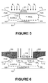
- the standard CMOS fabrication process may start with a P type semiconductor substrate, as illustrated in FIGURE 1. As illustrated in FIGURE 1, a P type semiconductor substrate 101 is initially covered with a photolithography mask 201. The photolithography mask 201 leaves a portion of the P-substrate 101 exposed, so that it may receive a first N type ion implant, as illustrated with respect to FIGURE 2.
- a first type ion implant is performed to implant a deep N-well 103.
- the N-well 103 is formed fairly deep in the substrate, so as to increase the sensitivity of the photodiode.
- the increase in sensitivity is achieved because the deep implant yields substantial increases in the photo response, due to an increase collection path for the instant photo-generated carriers.
- a photolithography mask 202 is deposited onto a portion of the P-substrate. Thereafter, a P type ion implant is performed to create a deep P-well 105 adjacent to the N-well 103. As will be described in more detail below, the P-well is used in part for the formation of a reset transistor, as well as a buffer transistor 151 and a row select transistor 153.
- field oxide regions 113 are formed in the substrate 101 using any suitable conventional semiconductor processing method, such as LOCOS.
- the field oxide regions 113 define an active area in which the photodiode is formed.
- an isolation oxide 115 is also formed on top of the substrate 101 between the field oxide regions 113.
- the isolation oxide 115 is also referred to as a gate oxide and is preferably formed from silicon dioxide.
- the method that is used to form the silicon dioxide isolation oxide layer 115 can be one of any well-known techniques, including the thermal oxidation of silicon.
- a layer of polysilicon 117 is deposited over the gate oxide 115.
- the polysilicon may be deposited using any conventional technique, such as low-pressure chemical vapor deposition (LPCVD).
- the polysilicon layer 117 is patterned and etched using conventional photolithography and masking techniques to form a control gate 121. As described below, this will be the gate 121 for the reset transistor.
- a doping step is performed.
- This doping step in one embodiment is an ion implantation of nitrogen (N 2 ).
- N 2 nitrogen
- the ion implantation process may be done after the gate 121 has been formed, or alternatively, the ion implantation may be performed before the gate oxide (isolation oxide 115) has been formed.
- the implant is performed at a power of 5-20 KeV and to a dosage of 1xE14 to 1xE16/cm 2 and to a depth of 100-500 angstroms.
- the ion implantation of nitrogen technique may damage the structures
- a conventional anneal process is performed to repair the damage.
- the nitrogen implant provides a nitrogen-passivated surface of the substrate 101.
- the photodiode that is formed is a N-well/P-sub type of photodiode, but other types of photodiodes may also be used. The important consideration is that the surface of the photodiode (whatever doped material is on the surface) is passivated.
- the doping step is performed by thermal diffusion of nitrogen into the substrate.
- the goal and result is the same as with the ion implantation: to passivate the dangling silicon bonds with nitrogen.
- the thermal diffusion is performed at 850-950 degrees C for about twenty minutes or more. Further, the thermal diffusion is optimally applied after the polysilicon gate 121 is patterned and etched, since it is difficult to diffuse nitrogen through polysilicon and gate oxide to the desired photodiode surface to passivate the dangling silicon bonds.
- any element that can passivate the dangling silicon bond may also be used.
- oxygen or hydrogen may be used.
- silicon may also be used, as well as any element that has strong bonding with the silicon substrate.
- thermal diffusion or ion implantation as techniques for doping.
- other types of doping such as low damage plasma doping.
- isolation oxide 115 which is typically formed from thermal silicon oxide (SiO 2 )
- SiO x N y silicon oxynitride
- FIGURE 4 instead of forming an isolation oxide 115, a silicon oxynitride layer is formed between the field oxide 113.
- the formation of silicon oxynitride is well known in the art and can be done using conventional chemical vapor deposition techniques.
- the use of silicon oxynitride, relative to silicon dioxide, provides fewer interface traps and replaces weak bonds near the Si-SiO 2 interface with stronger Si-N bonds.
- dark current can be reduced by using silicon oxynitride as the gate dielectric.
- a N 2 O-nitrided oxide has similar advantage to that of silicon oxynitride.
- a photolithography mask 203 is deposited.
- the mask 203 is formed using conventional lithography techniques.
- high concentration doping is used to form N+ regions using the mask 203 as an implementation mask.
- the implementation of the high concentration doping is performed using known techniques in the prior art and conventional dopants.
- This forms an N+ region 123 and an N+ region 125.
- the N+ region 123 is formed at the border between the N-well 103 and the P-well 105.
- the N+ regions 123 and 125 will be used as the source and drain of the reset transistor.
- the N+ region 123 is connected to output circuitry.
- the output circuitry includes a buffer transistor 151, in addition to a row select transistor 153.
- the N+ region 123 is coupled to the gate of the buffer transistor 151, while the drain of the buffer transistor 151 is coupled to a fixed voltage such as VDD.
- the source of the transistor 151 is coupled to the drain of the row select transistor 153, while the source of the transistor 153 provides the output of the processing circuitry.
- the gate of the row select transistor 153 receives a row select signal RS.
- the N+ region 125 is connected to a fixed voltage such as the supply voltage VDD.
- the reset gate 121 is periodically activated by a reset signal. When the reset signal is "on,” the channel under the reset gate 121 is made conducting, and current is able to flow through the transistor so as to reset the photodiode.
- the present invention provides an active pixel photodiode structure that can be formed with the standard CMOS process.
- the device of FIGURE 7 is formed with only three transistors, as compared to the four transistors required for the previously described pinned photodiodes.
- the present device can devote more area to photosensing rather than the processing circuitry.
- this avoids the image lag that can sometimes result in pinned photodiodes due to an incomplete transfer of charge from the diode to the floating node, in cases when the junction profile is not perfectly optimized for the charge transfer.
- the described structure of the present invention provides for a deep junction photodiode, as seen in the deep N-well/P-sub junction (as seen between the N-well 103 and the P-substrate 101), thereby providing for high sensitivity of the device.
- dark current is reduced in that a nitrogen (or other element) dopant passivates the silicon surface.
- FIGURES 2 and 3 While the preferred embodiment of the invention has been illustrated and described, it will be appreciated that various changed can be made therein without departing from the spirit and scope of the invention.
- the formation of the active pixel sensor illustrated in FIGURES 2 and 3 has generally shown the N-well 103 being formed before the P-well 105, these processes could be performed in the reverse order.
- the formation of the field oxide regions 113 in FIGURE 4 was generally illustrated as being formed after the N-well 103 and P-well 105, the N-well and/or P-well could be formed after the formation of the field oxide regions 113. It is also understood where the device has generally been shown using different types of P or N type materials, the types of materials could be switched to produce similar results.
- the alternate types of materials could be used to form a P-well/N-sub photodiode.
- the passivation techniques can also be used with photodiodes that are N+/P-well, N+/P-sub, N-well/P-sub, P+/N-well, P-well/N-sub, etc.
- the term PN photodiode is defined to include all types of photodiodes.
- the above-described photodiode could also be used in other applications.
- the photodiode could be implemented in a passive pixel sensor.
- other styles of active pixel sensors could be used, such as a two transistor, a four transistor, or a log scale implementation.
- some examples of general prior art design approaches to these other styles are shown in U.S. Patent Nos. 5,587,596, 5,926,214, and 5,933,190.
Landscapes
- Solid State Image Pick-Up Elements (AREA)
- Light Receiving Elements (AREA)
Abstract
Description
Claims (27)
- A pixel for use in a CMOS imaging array, said pixel having a PN photodiode comprising:a semiconductor substrate having a first conductivity type; anda well of a second conductivity type formed in the semiconductor substrate, the surface of said first well being passivated by a nitrogen dopant.
- The pixel of Claim 1, wherein said nitrogen dopant extends down from said surface by about 100-500 angstroms.
- The pixel of Claim 1, wherein said nitrogen dopant has a concentration of about 1xE14 to 1xE16/cm2.
- The pixel of Claim 1, further including a silicon oxide layer over said first well.
- The pixel of Claim 1, further including a silicon oxynitride layer over said first well.
- The pixel of Claim 1, wherein said nitrogen dopant is introduced using ion implantation.
- The pixel of Claim 1, wherein said nitrogen dopant is introduced using a thermal diffusion.
- The pixel of Claim 1, wherein said nitrogen dopant is replaced with an oxygen, hydrogen or silicon dopant.
- The pixel of Claim 8, wherein said oxygen dopant extends down from said surface by about 100-500 angstroms.
- The pixel of Claim 8, wherein said oxygen dopant has a concentration of about 1xE14 to 1xE16/cm2.
- The pixel of Claim 8, further including a silicon oxide layer over said first well.
- The pixel of Claim 8, further including a silicon oxynitride layer over said first well.
- A pixel for use in a CMOS image sensor comprising:a PN photodiode, the surface of said PN photodiode being passivated with a nitrogen dopant implant;a reset transistor coupled to the photodiode for resetting the signal level on the photodiode;a buffer transistor, the gate of the buffer transistor being coupled to the output of the photodiode; anda row select transistor, the gate of the row select transistor being coupled to a row select signal line, the input of the row select transistor being coupled to the output of the buffer transistor, and the output of the row select transistor providing the output of the pixel sensor cell.
- The pixel of Claim 13, wherein said nitrogen dopant is replaced with an oxygen, hydrogen, or silicon dopant.
- The pixel of Claim 13, wherein said nitrogen dopant extends down from said surface by about 100-500 angstroms.
- The pixel of Claim 13, wherein said nitrogen dopant has a concentration of about 1xE14 to 1xE16/cm2.
- The pixel of Claim 13, further including a silicon oxide layer over said first well.
- The pixel of Claim 13, further including a silicon oxynitride layer over said first well.
- A pixel for use in an image sensor comprising:a PN photodiode;a passivating silicon oxynitride layer formed over the surface of said PN photodiode;a reset transistor coupled to the PN photodiode for resetting the signal level on the photodiode;a buffer transistor, the gate of the buffer transistor being coupled to the output of the photodiode; anda row select transistor, the gate of the row select transistor being coupled to a row select signal line, the input of the row select transistor being coupled to the output of the buffer transistor, and the output of the row select transistor providing the output of the pixel sensor cell.
- A method for reducing dark current in a PN photodiode, said method comprising:doping the surface of said PN photodiode with a nitrogen dopant.
- The method of Claim 20 wherein said nitrogen dopant is replaced with an oxygen or silicon dopant.
- The method of Claim 20, wherein doping of said surface further extends down from said surface by about 100-500 angstroms.
- The method of Claim 20, wherein said nitrogen dopant has a concentration of about 1xE14 to 1xE16/cm2.
- The method of Claim 20, further including forming a silicon oxide layer over said N-well.
- The method of Claim 20, further including forming a silicon oxynitride layer over said N-well.
- The method of Claim 19, further including performing an annealing process after said doping step.
- A method for reducing dark current in a PN photodiode, said method comprising:forming a silicon oxynitride layer on the surface of said PN photodiode.
Applications Claiming Priority (2)
| Application Number | Priority Date | Filing Date | Title |
|---|---|---|---|
| US16271 | 1996-04-23 | ||
| US10/016,271 US6909162B2 (en) | 2001-11-02 | 2001-11-02 | Surface passivation to reduce dark current in a CMOS image sensor |
Publications (3)
| Publication Number | Publication Date |
|---|---|
| EP1309008A2 true EP1309008A2 (en) | 2003-05-07 |
| EP1309008A3 EP1309008A3 (en) | 2003-08-20 |
| EP1309008B1 EP1309008B1 (en) | 2007-05-16 |
Family
ID=21776271
Family Applications (1)
| Application Number | Title | Priority Date | Filing Date |
|---|---|---|---|
| EP02257518A Expired - Lifetime EP1309008B1 (en) | 2001-11-02 | 2002-10-30 | Surface passivation to reduce dark current in a CMOS image sensor |
Country Status (5)
| Country | Link |
|---|---|
| US (1) | US6909162B2 (en) |
| EP (1) | EP1309008B1 (en) |
| CN (1) | CN100492648C (en) |
| DE (1) | DE60220131T2 (en) |
| TW (1) | TWI220317B (en) |
Families Citing this family (24)
| Publication number | Priority date | Publication date | Assignee | Title |
|---|---|---|---|---|
| US7180798B2 (en) * | 2001-04-12 | 2007-02-20 | Fuji Electric Co., Ltd. | Semiconductor physical quantity sensing device |
| JP3974409B2 (en) * | 2002-01-22 | 2007-09-12 | 株式会社イシダ | Conveying device and boxing device provided with the same |
| CN100468753C (en) * | 2002-08-30 | 2009-03-11 | 皇家飞利浦电子股份有限公司 | Image sensor, camera system including the same, and method of manufacturing the same |
| KR100558528B1 (en) * | 2003-09-25 | 2006-03-10 | 동부아남반도체 주식회사 | CMOS image sensor and its manufacturing method |
| CN100369237C (en) * | 2004-07-29 | 2008-02-13 | 上海华虹Nec电子有限公司 | Technical method of front procedures for CMOS image sensor |
| KR101219038B1 (en) | 2004-10-26 | 2013-01-07 | 삼성디스플레이 주식회사 | Thin film transistor array panel and manufacturing method thereof |
| KR100621561B1 (en) * | 2004-11-05 | 2006-09-19 | 삼성전자주식회사 | CMOS image sensor and its driving method |
| US20080296644A1 (en) * | 2005-05-02 | 2008-12-04 | Samsung Electronics Co., Ltd. | Cmos image sensors and methods of fabricating same |
| KR100672812B1 (en) * | 2005-05-02 | 2007-01-22 | 삼성전자주식회사 | Image sensor and its manufacturing method |
| US20070063279A1 (en) * | 2005-09-16 | 2007-03-22 | Tolchinsky Peter G | Insulation layer for silicon-on-insulator wafer |
| KR100741877B1 (en) * | 2005-12-29 | 2007-07-23 | 동부일렉트로닉스 주식회사 | CMOS image sensor and its manufacturing method |
| US7544533B2 (en) * | 2006-01-09 | 2009-06-09 | Aptina Imaging Corporation | Method and apparatus for providing an integrated circuit having p and n doped gates |
| US7442974B2 (en) * | 2006-01-31 | 2008-10-28 | Hiok Nam Tay | Image sensor with inter-pixel isolation |
| US8053287B2 (en) * | 2006-09-29 | 2011-11-08 | Taiwan Semiconductor Manufacturing Company, Ltd. | Method for making multi-step photodiode junction structure for backside illuminated sensor |
| US20080211050A1 (en) * | 2007-03-01 | 2008-09-04 | Hiok Nam Tay | Image sensor with inter-pixel isolation |
| US8736726B2 (en) | 2007-06-27 | 2014-05-27 | Micron Technology, Inc. | Pixel to pixel charge copier circuit apparatus, systems, and methods |
| US20100013039A1 (en) * | 2008-07-21 | 2010-01-21 | Omnivision Technologies, Inc. | Backside-illuminated imaging sensor including backside passivation |
| US9153621B2 (en) * | 2010-01-12 | 2015-10-06 | Himax Imaging, Inc. | Process of forming a back side illumination image sensor |
| US9013612B2 (en) | 2010-08-20 | 2015-04-21 | Semiconductor Components Industries, Llc | Image sensors with antireflective layers |
| US8760543B2 (en) | 2011-09-26 | 2014-06-24 | Truesense Imaging, Inc. | Dark reference in CCD image sensors |
| US10134926B2 (en) | 2015-02-03 | 2018-11-20 | Microsoft Technology Licensing, Llc | Quantum-efficiency-enhanced time-of-flight detector |
| US9923003B2 (en) | 2015-06-30 | 2018-03-20 | Microsoft Technology Licensing, Llc | CMOS image sensor with a reduced likelihood of an induced electric field in the epitaxial layer |
| CN106052857B (en) * | 2016-08-22 | 2017-12-01 | 成都三零嘉微电子有限公司 | A kind of photoelectric detective circuit with temperature compensation function |
| US11700464B2 (en) * | 2020-01-09 | 2023-07-11 | Omnivision Technologies, Inc. | Selective nitrided gate-oxide for RTS noise and white-pixel reduction |
Family Cites Families (10)
| Publication number | Priority date | Publication date | Assignee | Title |
|---|---|---|---|---|
| JPS5642377A (en) * | 1979-09-14 | 1981-04-20 | Fujitsu Ltd | Ultraviolet ray erasable type rewritable read-only memory |
| JPS5696877A (en) * | 1979-12-30 | 1981-08-05 | Shunpei Yamazaki | Photoelectric converter |
| JPS61294866A (en) | 1985-06-21 | 1986-12-25 | Nippon Texas Instr Kk | Charge-coupled type semiconductor device |
| US5394005A (en) * | 1992-05-05 | 1995-02-28 | General Electric Company | Silicon carbide photodiode with improved short wavelength response and very low leakage current |
| DE19632627A1 (en) * | 1996-08-13 | 1998-02-19 | Siemens Ag | Method for producing a light-emitting and / or receiving semiconductor body |
| JP3602679B2 (en) | 1997-02-26 | 2004-12-15 | 株式会社ルネサステクノロジ | Semiconductor device and manufacturing method thereof |
| US6232626B1 (en) * | 1999-02-01 | 2001-05-15 | Micron Technology, Inc. | Trench photosensor for a CMOS imager |
| US6339248B1 (en) | 1999-11-15 | 2002-01-15 | Omnivision Technologies, Inc. | Optimized floating P+ region photodiode for a CMOS image sensor |
| US6235600B1 (en) | 2000-03-20 | 2001-05-22 | Taiwan Semiconductor Manufacturing Company | Method for improving hot carrier lifetime via a nitrogen implantation procedure performed before or after a teos liner deposition |
| US6271054B1 (en) | 2000-06-02 | 2001-08-07 | International Business Machines Corporation | Method for reducing dark current effects in a charge couple device |
-
2001
- 2001-11-02 US US10/016,271 patent/US6909162B2/en not_active Expired - Lifetime
-
2002
- 2002-10-30 DE DE60220131T patent/DE60220131T2/en not_active Expired - Lifetime
- 2002-10-30 TW TW091132213A patent/TWI220317B/en not_active IP Right Cessation
- 2002-10-30 EP EP02257518A patent/EP1309008B1/en not_active Expired - Lifetime
- 2002-11-04 CN CNB021575762A patent/CN100492648C/en not_active Expired - Lifetime
Also Published As
| Publication number | Publication date |
|---|---|
| US20030086011A1 (en) | 2003-05-08 |
| DE60220131D1 (en) | 2007-06-28 |
| EP1309008B1 (en) | 2007-05-16 |
| TWI220317B (en) | 2004-08-11 |
| US6909162B2 (en) | 2005-06-21 |
| CN1419296A (en) | 2003-05-21 |
| TW200302572A (en) | 2003-08-01 |
| EP1309008A3 (en) | 2003-08-20 |
| DE60220131T2 (en) | 2008-01-24 |
| CN100492648C (en) | 2009-05-27 |
Similar Documents
| Publication | Publication Date | Title |
|---|---|---|
| US6909162B2 (en) | Surface passivation to reduce dark current in a CMOS image sensor | |
| US6486521B2 (en) | Optimized floating P+ region photodiode for a CMOS image sensor | |
| US7368772B2 (en) | Active pixel having reduced dark current in a CMOS image sensor | |
| US6512280B2 (en) | Integrated CMOS structure for gate-controlled buried photodiode | |
| US7960765B2 (en) | Method and apparatus for providing an integrated circuit having p and n doped gates | |
| US5705846A (en) | CMOS-compatible active pixel image array using vertical pnp cell | |
| US8367457B2 (en) | Polydiode structure for photo diode | |
| US7205641B2 (en) | Polydiode structure for photo diode | |
| US20040017496A1 (en) | Solid state image pickup device and manufacturing method therefor | |
| US6392263B1 (en) | Integrated structure for reduced leakage and improved fill-factor in CMOS pixel | |
| US6306679B1 (en) | Photodiode having transparent insulating film around gate islands above P-N junction | |
| US6492668B2 (en) | Solid imaging device and production method thereof | |
| US6350127B1 (en) | Method of manufacturing for CMOS image sensor | |
| US5576237A (en) | Method of manufacturing a capacitor coupled contactless imager with high resolution and wide dynamic range | |
| US20020162945A1 (en) | CMOS photodiode having reduced dark current and improved light sensitivity and responsivity | |
| US7105878B2 (en) | Active pixel having reduced dark current in a CMOS image sensor | |
| US5837574A (en) | Method of manufacturing a thin poly, capacitor coupled contactless imager with high resolution and wide dynamic range | |
| KR100776151B1 (en) | Highly integrated image sensor manufacturing method | |
| EP1746656A2 (en) | Pixel sensor with raised silicon photodiode | |
| KR20060059545A (en) | Image sensor and its manufacturing method |
Legal Events
| Date | Code | Title | Description |
|---|---|---|---|
| PUAI | Public reference made under article 153(3) epc to a published international application that has entered the european phase |
Free format text: ORIGINAL CODE: 0009012 |
|
| AK | Designated contracting states |
Designated state(s): AT BE BG CH CY CZ DE DK EE ES FI FR GB GR IE IT LI LU MC NL PT SE SK TR |
|
| AX | Request for extension of the european patent |
Extension state: AL LT LV MK RO SI |
|
| PUAL | Search report despatched |
Free format text: ORIGINAL CODE: 0009013 |
|
| AK | Designated contracting states |
Designated state(s): AT BE BG CH CY CZ DE DK EE ES FI FR GB GR IE IT LI LU MC NL PT SE SK TR |
|
| AX | Request for extension of the european patent |
Extension state: AL LT LV MK RO SI |
|
| 17P | Request for examination filed |
Effective date: 20030722 |
|
| 17Q | First examination report despatched |
Effective date: 20040206 |
|
| AKX | Designation fees paid |
Designated state(s): AT BE BG CH CY CZ DE DK EE ES FI FR GB GR IE IT LI LU MC NL PT SE SK TR |
|
| GRAP | Despatch of communication of intention to grant a patent |
Free format text: ORIGINAL CODE: EPIDOSNIGR1 |
|
| GRAS | Grant fee paid |
Free format text: ORIGINAL CODE: EPIDOSNIGR3 |
|
| RBV | Designated contracting states (corrected) |
Designated state(s): DE FR GB |
|
| GRAA | (expected) grant |
Free format text: ORIGINAL CODE: 0009210 |
|
| AK | Designated contracting states |
Kind code of ref document: B1 Designated state(s): DE FR GB |
|
| REG | Reference to a national code |
Ref country code: GB Ref legal event code: FG4D |
|
| REF | Corresponds to: |
Ref document number: 60220131 Country of ref document: DE Date of ref document: 20070628 Kind code of ref document: P |
|
| ET | Fr: translation filed | ||
| PLBE | No opposition filed within time limit |
Free format text: ORIGINAL CODE: 0009261 |
|
| STAA | Information on the status of an ep patent application or granted ep patent |
Free format text: STATUS: NO OPPOSITION FILED WITHIN TIME LIMIT |
|
| 26N | No opposition filed |
Effective date: 20080219 |
|
| REG | Reference to a national code |
Ref country code: FR Ref legal event code: PLFP Year of fee payment: 15 |
|
| REG | Reference to a national code |
Ref country code: FR Ref legal event code: PLFP Year of fee payment: 16 |
|
| REG | Reference to a national code |
Ref country code: FR Ref legal event code: PLFP Year of fee payment: 17 |
|
| PGFP | Annual fee paid to national office [announced via postgrant information from national office to epo] |
Ref country code: FR Payment date: 20210921 Year of fee payment: 20 |
|
| PGFP | Annual fee paid to national office [announced via postgrant information from national office to epo] |
Ref country code: GB Payment date: 20210929 Year of fee payment: 20 |
|
| PGFP | Annual fee paid to national office [announced via postgrant information from national office to epo] |
Ref country code: DE Payment date: 20210916 Year of fee payment: 20 |
|
| REG | Reference to a national code |
Ref country code: DE Ref legal event code: R071 Ref document number: 60220131 Country of ref document: DE |
|
| REG | Reference to a national code |
Ref country code: GB Ref legal event code: PE20 Expiry date: 20221029 |
|
| PG25 | Lapsed in a contracting state [announced via postgrant information from national office to epo] |
Ref country code: GB Free format text: LAPSE BECAUSE OF EXPIRATION OF PROTECTION Effective date: 20221029 |