EP1308899A2 - Image processing apparatus - Google Patents
Image processing apparatus Download PDFInfo
- Publication number
- EP1308899A2 EP1308899A2 EP02292652A EP02292652A EP1308899A2 EP 1308899 A2 EP1308899 A2 EP 1308899A2 EP 02292652 A EP02292652 A EP 02292652A EP 02292652 A EP02292652 A EP 02292652A EP 1308899 A2 EP1308899 A2 EP 1308899A2
- Authority
- EP
- European Patent Office
- Prior art keywords
- data
- memory
- built
- circuit
- texture
- Prior art date
- Legal status (The legal status is an assumption and is not a legal conclusion. Google has not performed a legal analysis and makes no representation as to the accuracy of the status listed.)
- Withdrawn
Links
Images






Classifications
-
- G—PHYSICS
- G06—COMPUTING OR CALCULATING; COUNTING
- G06T—IMAGE DATA PROCESSING OR GENERATION, IN GENERAL
- G06T15/00—Three-dimensional [3D] image rendering
- G06T15/005—General purpose rendering architectures
Definitions
- the present invention relates to a graphics drawing image processing apparatus, more particularly relates to technology for accessing a built-in memory and external memory when combining a dynamic random access memory (DRAM) or other memory requiring refreshing and a logic circuit and further providing an external memory.
- DRAM dynamic random access memory
- Computer graphics are often used in a variety of computer aided design (CAD) system and amusement apparatuses. Especially, along with recent advances in image processing techniques, systems using three-dimensional computer graphics are becoming rapidly widespread.
- CAD computer aided design
- the color value of each pixel is calculated at the time of deciding the color of each corresponding pixel, and rendering is performed for writing the calculated value of the pixel to an address of a display buffer (frame buffer) corresponding to the pixel.
- One of the rendering methods is polygon rendering.
- a three-dimensional model is expressed as a composite of triangular unit graphics (polygons). By drawing the polygons as units, the colors of the display screen are decided.
- the coordinates in a UV coordinate system of an actual texture buffer namely, texture coordinate data (u, v) are comprised of the homogeneous coordinates (s, t) divided by the homogeneous term q to give "s/q” and "t/q” which in turn are multiplied by texture sizes USIZE and VSIZE, respectively.
- FIG. 12 is a view of the system configuration showing the basic concept of a three-dimensional computer graphics system.
- data for drawing graphics is supplied from a main memory 2 in a main processor 1 or from an input/output (I/O) interface circuit 3 for receiving graphics data from the outside via a main bus 4 to a rendering circuit 5 having a rendering processor 5a and a frame buffer memory 5b.
- I/O input/output
- a frame buffer memory 5b for holding data for display and a texture memory 6 for holding texture data to be applied on the surface of a graphic element (for example, triangle) to be drawn are connected.
- the frame buffer memory 5b and the texture memory 6 are generally configured by a DRAM.
- the frame buffer memory 5b and the texture memory 6 are configured as physically separated memory systems.
- the memory is frequently accessed such as for writing and reading image data to and from the memory and for reading for display of the image. Further, it becomes necessary to secure a wide bus width of the memory to obtain the full graphics drawing performance.
- the memory is frequently accessed for being rewritten from the outside due to the shortage of the memory capacity. This exerts a large influence upon the performance.
- An object of the present invention is to provide an image processing apparatus capable of achieving an increase of capacity and accordingly capable of achieving an improvement of the processing capability without causing a drop in performance or an increase of costs.
- an image processing apparatus comprising at least a built-in memory for storing image data, an external memory for storing data regarding the image, a logic circuit provided on the same semiconductor chip as the built-in memory and performing predetermined processing on the image data based on the stored data of the built-in memory and/or external memory, and a memory interface circuit for controlling access of data between the built-in memory and external memory and the logic circuit.
- an image processing apparatus for performing rendering by receiving polygon rendering data including three-dimensional coordinates (x, y, z), R (Red), G (Green), and B (Blue) data, homogeneous coordinates (s, t) of texture, and a homogeneous term q for vertices of a unit graphic, comprising a built-in memory for storing display data and texture data required by at least one graphic element; a logic circuit provided with at least an interpolated data generation circuit for interpolating the polygon rendering data of the vertices of the unit graphic to generate interpolated data of pixels positioned inside the unit graphic and a texture processing circuit for dividing the homogeneous coordinates (s, t) of texture included in the interpolated data by the homogeneous term q to generate "s/q" and "t/q", reading texture data by using a texture address corresponding to the "s/q” and "t/q", and performing processing to apply the texture data to a surface
- the built-in memory stores the data having high access frequency
- the memory interface circuit accesses the stored data of the built-in memory prior to the stored data of the external memory and supplies the data to the logic circuit.
- the capacity of the external memory is larger than the capacity of the built-in memory
- the memory area of the external memory is divided into a plurality of blocks
- predetermined data is stored in individual blocks
- the memory area of the built-in memory is divided into blocks each having the same capacity as a divided block of the external memory
- the memory interface circuit accesses the data stored in each divided block in the built-in memory and supplies the data to the logic circuit and further receives a displacement command and displaces data which becomes unnecessary among the data stored in the built-in memory with the data needed next stored in the predetermined blocks of the external memory.
- the built-in memory stores data regarding an image having a high access frequency
- the external memory stores data having a low access frequency. Accordingly, in normal image processing, the memory interface circuit frequently accesses the built-in memory and accesses the external memory in accordance with need.
- the capacity of the external memory is set larger than the capacity of the built-in memory.
- the memory area of the external memory is divided into a plurality of blocks and the predetermined data is stored in individual blocks.
- the memory area of the built-in memory is divided into blocks each having the same capacity as that of a divided block of the external memory.
- the data which becomes necessary newly stored in the built-in memory is accessed by the memory interface circuit and supplied to the block circuit.
- FIG. 1 is a view of the system configuration of a three-dimensional computer graphics system 10 as an image processing apparatus according to the present invention.
- the three-dimensional computer graphics system 10 expresses a three-dimensional model as a composite of triangular unit graphics (polygons). By drawing the polygons, the colors of the pixels of the display screen are decided and polygon rendering for display on the display is performed.
- a three-dimensional object is expressed by using a z-coordinate indicating depth in addition to the coordinates (x, y) indicating a position on a plane.
- the three coordinates (x, y, z) specify any one point in a three-dimensional space.
- the three-dimensional computer graphics system 10 has a main processor 11, a main memory 12, an I/O interface circuit 13, a rendering circuit 14, and an external memory 15.
- main processor 11, main memory 12, I/O interface circuit 13, and the rendering circuit 14 are connected via a main bus 16.
- the main processor 11 reads the necessary graphics data from the main memory 12 in accordance with, for example, the state of progress of an application and performs clipping, lighting, and geometric processing etc. on the graphics data and generates polygon rendering data.
- the main processor 11 outputs the polygon rendering data S11 to the rendering circuit 14 via the main bus 16.
- the I/O interface circuit 13 receives as input the motion control information or the polygon rendering data from the outside in accordance with need and outputs the same to the rendering circuit 14 via the main bus 16.
- the polygon rendering data includes the data (x, y, z, R, G, B, s, t, q) of each of the three vertices of the polygon.
- the (x, y, z) data indicates the three-dimensional coordinates of a vertex of the polygon
- (R, G, B) indicates the luminance values of red, green, and blue at the three-dimensional coordinates, respectively.
- the (s, t) indicates homogeneous coordinates of a corresponding texture and the q indicates a homogeneous term.
- the texture sizes USIZE and VSIZE are respectively multiplied with the "s/q" and "t/q" to obtain the texture coordinate data (u, v).
- the access to the texture data stored in the texture buffer is performed by using the texture coordinate data (u, v).
- the polygon rendering data comprises physical coordinate values of the vertices of a triangle and colors and texture data of each of the vertices.
- the rendering circuit 14 comprises a digital differential analyzer (DDA) set-up circuit 141, a triangle DDA circuit 142, a texture engine circuit 143, a memory interface (I/F) circuit 144 including a function as a refresh circuit, a CRT control circuit 145, a RAMDAC circuit 146, a DRAM 147, and a static RAM (SRAM) 148.
- DDA digital differential analyzer
- the rendering circuit 14 in the present embodiment is provided with a logic circuit and a DRAM 147 for storing at least display data and texture data in one semiconductor chip.
- the configuration of the DRAM 147, and the function of the memory I/F circuit 144 including the access control of the DRAM 147 and the external memory 15 will be explained first. Then, the functions of the DDA set-up circuit 141, the triangle DDA circuit 142, the texture engine circuit 143, a CRT control circuit 145, and the RAMDAC circuit 146 will be explained in that order.
- the DRAM 147 functions as a texture buffer 147a, a display buffer 147b, a z-buffer 147c, and a texture color look-up table (CLUT) buffer 147d.
- CLUT texture color look-up table
- the DRAM 147 is divided into a plurality of modules (4 or 8 etc.) having identical functions.
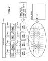
- the DRAM 147 is, for example as shown in FIG. 2, divided into four DRAM modules 1471 to 1474.
- Each of the DRAM modules 1471 to 1474 has, for example, 512 page addresses (line addresses).
- the memory I/F circuit 144 is provided with memory controllers 1441 to 1444 corresponding to the DRAM modules 1471 to 1474 and a distributor 1445 for distributing data to the memory controllers 1441 to 1444.
- the memory I/F circuit 144 arranges the pixel data in the DRAM modules 1471 to 1474 so that adjacent portions in a display region are stored in different DRAM modules as shown in FIG. 2.
- the DRAM 147 stores indexes in index colors and color look-up table values for the same in the texture CLUT buffer 147d.
- the indexes and color look-up table values are used for texture processing. Namely, a texture element is normally expressed by the total 24 bits of the 8 bits of each of R, G, and B. With this, however, the amount of data swells, so one color is selected from, for example, 256 colors selected in advance and that data is used for the texture processing. As a result, with 256 colors, the texture elements can be expressed by 8 bits. A conversion table from the indexes to an actual color is necessary, however, the higher the resolution of the texture, the more compact the texture data can become.
- depth information of the object to be drawn is stored in the DRAM 147 in order to perform hidden plane processing simultaneously and in parallel with the drawing.
- the display data is stored continuously from the top of the memory block, then the depth data is stored, and then the texture data is stored in continuous address spaces for each type of texture in the remaining vacant region.
- the texture data can be stored efficiently.
- the graphics drawing processing is finally reduced to access the individual pixels. Accordingly, ideally, the processings of the individual pixels are simultaneously processed in parallel, whereby the graphics drawing performance can be increased by exactly the number of parallel processings.
- the memory I/F circuit 144 compares the z-data corresponding to the pixel data S143 input from the texture engine circuit 143 with the z-data stored in the z-buffer 147c, judges whether the image drawn by the input pixel data S143 is positioned closer to the viewing point than the image written in the display buffer 147b the previous time, and, when judging that it is positioned closer, updates the z-data stored in the z-buffer 147c by the z-data corresponding to the image data S143.
- the memory I/F circuit 144 writes (inputs) (R, G, B) data to the display buffer 147b.
- the memory I/F circuit 144 accesses the DRAM 147 for 16 pixels simultaneously.
- the memory I/F circuit 144 accesses the external memory 15 in parallel to accessing the built-in DRAM 147.
- the external memory 15 comprising the DRAM is used as the interpolative memory of the built-in DRAM 147 and has for example texture data stored therein.
- the memory I/F circuit 144 can selectively use the external memory 15 and the built-in DRAM 147 in two ways as shown below.
- FIG. 3 there is the method of allocating a memory area MA1 to the built-in memory (DRAM) 147 and simply allocating the external memory 15 as a memory area MA2 for a memory space (address) exceeding the memory area MA1 of the built-in memory 147.
- DRAM built-in memory
- the memory I/F circuit 144 accesses the stored data of the built-in memory 147 prior to the stored data of the external memory 15.
- the external memory 15 can have a much larger capacity than the built-in memory 147.
- the functions of dividing the external memory 15 into several blocks, similarly dividing the built-in memory into blocks of the same capacities as those of those blocks, and flexibly displacing these by a command from the main processor 11 are imparted to the memory I/F circuit 144, whereby the memory system may be more efficiently administered.
- the address spaces of the built-in memory 147 and the data stored there are assumed to be as shown in FIG. 4A.
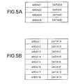
- the memory I/F circuit 144 immediately transfers the data and prepares for the necessity of the data "1E".
- the contents of the built-in memory 147 and the external memory 15 become as shown in FIGS. 5A and 5B.
- the DDA set-up circuit 141 Before the succeeding triangle DDA circuit 142 linearly interpolates the values of the vertices of a triangle in a physical coordinate system to obtain information of the color and depth of pixels inside the triangle, the DDA set-up circuit 141 performs the set-up operation for obtaining the difference with a side of the triangle in the horizontal direction etc. for the data (z, R, G, B, s, t, q) indicated by the polygon rendering data S11.
- this set-up operation uses values of a starting point and end point and the distance between the starting point and end point to calculate the change of values being sought in the case of movement by a unit length.
- the DDA set-up circuit 141 outputs the calculated change data S141 to the triangle DDA circuit 142.
- the main processing of the DDA set-up circuit 141 obtains the change inside a triangle composed of three vertices given various information (color and texture coordinates) at vertices reduced to physical coordinates through previous geometric processing so as to calculate basic data for the later linear interpolation.
- the direction of drawing is made constant in one triangle.
- the X with respect to displacement in the Y direction at a side on the left and the above various changes are calculated first, then these are used to find the x-coordinate of the leftmost point when moving from a vertex to the next horizontal line and values of the above various information (points on a side change in both the x- and y-directions, so calculation is impossible only from the gradient of the Y direction).
- the given triangle is sorted in the Y direction and the uppermost point is set to be A.
- the remaining two vertices are compared in terms of the positions in the X direction and the point on the right is set to be B.
- the triangle DDA circuit 142 uses the change data S141 input from the DDA set-up circuit 141 to calculate the linearly interpolated (z, R, G, B, s, t, q) data for each pixel inside the triangle.
- the triangle DDA circuit 142 outputs the data (x, y) for each pixel and the (z, R, G, B, s, t, q) data at the (x, y) coordinates to the texture engine circuit 143 as the DDA data (interpolated data) S142.
- gradient information of the above various information of the sides and horizontal direction of a triangle is prepared by the DDA set-up circuit 141.
- the basic processing of the triangle DDA circuit 142 receiving this information comprises the calculation of the initial values of the horizontal line by interpolation of the various information of the sides of the triangle and the interpolation of the various information on the horizontal line.
- the various information at the leftmost side of a first horizontal line can be obtained by multiplying the gradient on the side with the distance from the vertex to the first horizontal line.
- the various information at the starting point of the next line can be calculated by adding the gradient of the side.
- the value at the first pixel of the horizontal line can be calculated by adding the value obtained by multiplying the distance to the first pixel with the gradient in the horizontal direction to the value at the starting point of the line.
- the value at the next pixel of the horizontal line can be calculated by adding to the first pixel value the gradient in the horizontal direction successively.
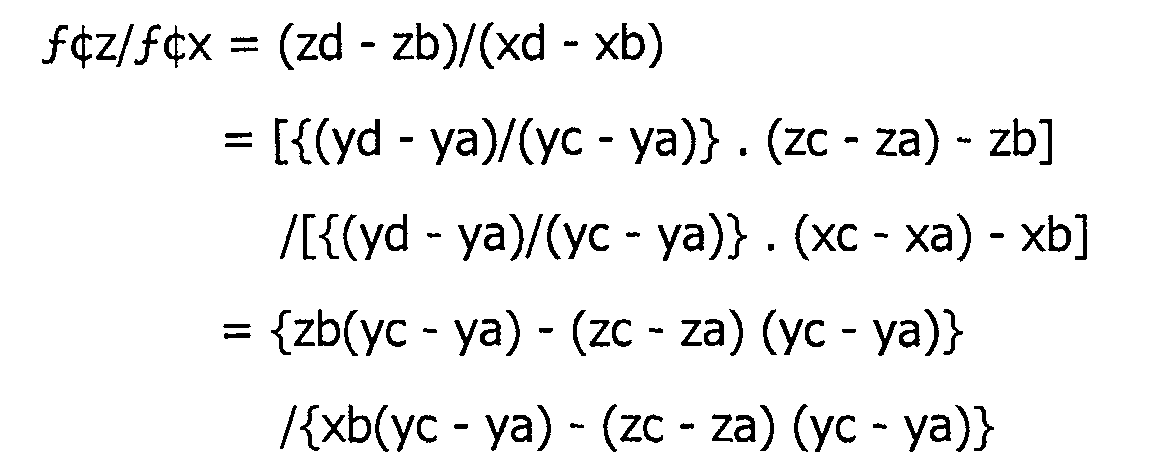
- the side extending the longest in the Y direction becomes a side AC.
- the side AC and the side AB are used for the interpolation of the region between the two sides, then interpolation is performed for the region between the side BC and the side AC, that is, leaving the side AC as it is and changing from the side AB. Further, it will be understood that it is sufficient to perform processing with respect to the side AC and the side BC for correction on the pixel coordinate lattice in the Y direction.
- the direction of the interpolation in one triangle can be made constant by setting a starting point on the side BC, the direction of interpolation (span) in the horizontal direction becomes constant, and any processing errors which occur are accumulated from the side BC to other sides. Since the direction of the accumulation becomes constant, errors between adjacent sides become less conspicuous.
- the gradient in the horizontal direction that is, the gradient on each of the horizontal lines (span) becomes constant for all spans, so the gradient is obtained prior to the processing of the spans.
- the side AC is defined again to be the longest extending side, so there is always a point of intersection of a line extending from the vertex B in the horizontal direction and the side AC. This point is defined as D.
- the processing at a span splits in two directions. This is because it is desired to perform the processing by always using the side extending the longest in the Y direction as a starting point so as to try to prevent trouble as much as possible by making the direction of accumulation of errors between spans in interpolation inside one triangle constant.
- the processing can be streamlined by just providing a skippable mechanism rather than branching.
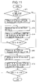
- steps ST3 and ST4 are performed until the end of the side AB (ST5).
- step ST6 the Y direction correction of BC (calculation of values on the pixel lattice) is carried out (ST6) and the interpolation on the side AC and the interpolation on the side BC are carried out (ST7).
- the texture engine circuit 143 performs the calculation of "s/q” and "t/q”, the calculation of the texture coordinate data (u, v), and the reading of the (R, G, B) data from the texture buffer 147a in order in a pipeline format.
- the texture engine circuit 143 performs processing on the 8 pixels positioned inside a predetermined block simultaneously in parallel.
- the texture engine circuit 143 performs the operation for dividing the data s by the data q and the operation for dividing the data t by the data q on the (s, t, q) data indicated by the DDA data S142.
- the texture engine circuit 143 is provided with, for example, eight division circuits, not illustrated, and performs the division "s/q" and "t/q" simultaneously on the 8 pixels.
- the texture engine circuit 143 respectively multiplies the texture sizes USIZE and VSIZE with the division results "s/q" and "t/q” to generate the texture coordinate data (u, v).
- the texture engine circuit 143 outputs a read request including the generated texture coordinate data (u, v) to the SRAM 148 or DRAM 147 via the memory I/F circuit 144.
- the texture engine circuit 143 obtains the (R, G, B) data S148 stored at the texture address corresponding to the (s, t) data by reading the texture data stored in the SRAM 148 or in the texture buffer 147a via the memory I/F circuit 144.
- the texture data stored in the texture buffer 147a is stored in the SRAM 148 as explained above.
- the texture engine circuit 143 generates pixel data S143 by multiplying etc. the (R, G, B) data in the read (R, G, B) data S148 and the (R, G, B) data included in the DDA data S142 from the former triangle DDA circuit 142.
- the texture engine circuit 143 outputs the pixel data S143 to the memory I/F circuit 144.
- MIPMAP texture for a plurality of resolutions
- other texture data corresponding to a plurality of reducing rates is stored.
- which reducing rate texture data to use is determined in the above triangular units using a predetermined algorithm.
- the texture engine circuit 143 directly uses the (R, G, B) data read from the texture buffer 147a.
- the texture engine circuit 143 reads a color look-up table (CLUT), prepared in advance, from the texture CLUT buffer 147d, transfers and stores the same in the built-in SRAM, and uses the color look-up table to obtain the (R, G, B) data corresponding to the color index read from the texture buffer 147a.
- CLUT color look-up table
- the CRT control circuit 145 generates an address for display on a not shown CRT in synchronization with given horizontal and vertical synchronization signals and outputs a request for reading the display data from the display buffer 147b to the memory I/F circuit 144. In response to this request, the memory I/F circuit 144 reads a certain amount of the display data from the display buffer 147b.
- the CRT controller circuit 145 has a built-in first-in first-out (FIFO) circuit for storing the display data read from the display buffer 147b and outputs the index value of RGB to the RAMDAC circuit 146 at certain time intervals.
- FIFO first-in first-out
- the RAMDAC circuit 146 stores the R, G, B data corresponding to the index values. It transfers R, G, B data of a digital format corresponding to the index value of RGB input from the CRT controller circuit 145 to a not illustrated digital/analog (D/A) converter to generate R, G, B data of an analog format. The RAMDAC circuit 146 outputs the generated R, G, B data to the not illustrated CRT.
- D/A digital/analog
- data for drawing graphics etc. are supplied from the main memory 12 of the main processor 11 or from the I/O interface circuit 13, which receives graphics data from the outside, to the rendering circuit 14 via the main bus 16.
- the graphics data after the geometric processing becomes polygon rendering data S11 composed of the coordinates x, y, z of the three vertices of a triangle, the luminance values R, G, B, the texture coordinates s, t, q corresponding to the pixel to be drawn, etc.
- the polygon rendering data S11 is input to the DDA set-up circuit 141 of the rendering circuit 14.
- change data S141 indicating the difference of a side of the triangle from a horizontal direction etc. is generated based on the polygon rendering data S11. Specifically, the change, that is, the amount of change of the values to be obtained in the case of movement by a unit length, is calculated by using the value of the starting point, the value of the end point, and the distance between the two and output to the triangle DDA circuit 142 as change data S141.
- the change data S141 is used for calculation of the linearly interpolated data (z, R, G, B, s, t, q) of each of the pixels inside the triangle.
- the calculated (z, R, G, B, s, t, q) data and the (x, y) data of each of the vertices of the triangle are output from the triangle DDA circuit 142 to the texture engine circuit 143 as DDA data S142.
- the operation for dividing the data s by the data q and the operation for dividing the data t by data q are performed for the (s, t, q) data indicated by the DDA data S142. Then, the texture sizes USIZE and VSIZE are respectively multiplied with the division results "s/q" and "t/q” to generate the texture coordinate data (u, v).
- a read request including the generated texture coordinate data (u, v) is output from the texture engine circuit 143 to the SRAM 148 via the memory I/F circuit 144, and the (R, G, B) data S148 stored in the SRAM 148 is read via the memory I/F circuit 144.
- the (R, G, B) data in the read (R, G, B) data S148 and the (R, G, B) data included in the DDA data S142 from the triangle DDA circuit 142 in the former stage are multiplied to generate the pixel data S143.
- This pixel data S143 is output from the texture engine circuit 143 to the main memory I/F circuit 144.
- the (R, G, B) data read from the texture buffer 147a can be directly used, while in the case of an index color mode, data in the color look-up table (CLUT), prepared in advance, is transferred from the texture CLUT buffer 147d to a buffer for temporary storage, which is configured by an SRAM etc.
- CLUT color look-up table
- the z-data corresponding to the pixel data S143 input from the texture engine circuit 143 and the z-data stored in the z-buffer 147c are compared for judging whether the image drawn by the input pixel data S143 is positioned closer to the viewing point than the image written in the display buffer 21 the previous time.
- the z-data stored in the z-buffer 147c is replaced by the z-data corresponding to the image data S143.
- the (R, G, B) data is written in the display buffer 147b.
- the memory block storing the texture corresponding to the texture address of the pixel to be drawn is calculated from the texture address, a read request is made only to the memory block, and the texture data is read.
- a memory block storing pixel data corresponding to a pixel address to be drawn is accessed to read the pixel data from the corresponding address for modify writing, the data is modified, then is written back to the same address.
- a memory block storing depth data corresponding to a pixel address to be drawn is accessed to read the depth data from the corresponding address for modify writing, the data is modified if necessary, then is written back to the same address.
- a plurality of pixels can be simultaneously calculated by the means of partially increasing the operating frequency by providing the triangle DDA circuit 142 and the texture engine 143 portions in the same circuit in a parallel execution mode (spatial parallel) or by inserting a lot of pipelines (time parallel).
- the data which becomes unnecessary among the data stored in the built-in DRAM 147 is displaced with the data needed next stored in the predetermined block of the external memory 15.
- the pixel data is arranged so that the adjacent portions in the display region are in different DRAM modules under the control of the memory I/F circuit 144.
- the CRT control circuit 145 When displaying an image on a not illustrated CRT, the CRT control circuit 145 generates the display address in synchronization with the given horizontal and vertical synchronization frequencies and sends a request for transferring the display data to the memory I/F circuit 144.
- the memory I/F circuit 144 in accordance with a request, transfers a certain amount of the display data to the CRT control circuit 145.
- the CRT control circuit 145 stores the display data in a not illustrated display use first-in first-out (FIFO) etc. and transfers index values of RGB to the RAMDAC 146 at certain intervals.
- FIFO display use first-in first-out
- the RAMDAC 146 stores the RGB values with respect to RGB indexes inside the RAM and transfers the RGB values with respect to the index values to a not illustrated D/A converter.
- the RGB signal converted into an analog signal by the D/A converter is transferred to the CRT.
- the external memory 15 is additionally provided, the capacity of the external memory 15 is set larger than the capacity of the built-in memory 147, the memory area of the external memory 15 is divided into a plurality of blocks and the predetermined data is stored in each of the blocks, the memory area of the built-in memory 147 is divided into blocks each having the same capacity as that of the divided block of the external memory 15, the memory I/F circuit 144 displaces the data which becomes unnecessary among the data stored in the built-in memory with the data to be needed next stored in the predetermined block of the external memory when certain data stored in the built-in memory becomes unnecessary and the displacement command is issued, and the data which becomes necessary newly stored in the built-in memory 147 is accessed by the memory I/F circuit 144, so not only can the capacity be greatly increased, but also the advantages of the built-in memory of fast processing speed and reaction speed can be sufficiently exhibited.
- the system can be efficiently administered, and a three-dimensional graphics system of a high processing capability can be constructed at a low cost by using the external memory of the optimum capacity corresponding to the system.
- the DRAM 147 built inside the semiconductor chip is configured to store display data and texture data required by at least one graphic element, it becomes possible to store the texture data in a portion other than a display region.
- the built-in DRAM can be effectively used and an image processing apparatus capable of attaining both a high speed processing operation and a low power consumption can be realized.
- the memory can be efficiently used, processing only by the DRAM provided therein becomes possible, and the large bandwidth between the memory and the drawing system due to the internal provision can be sufficiently utilized. Further, special processing can be built into the DRAM.
- indexes in index color and color look-up table values therefore are stored inside the built-in DRAM 147 to enable storage of more texture data, compression of the texture data becomes possible and the built-in DRAM can be effectively used.
- a graphic is drawn and then displayed, but it is also possible not to use it directly for display, but to use the drawn data as texture data because the texture data and display data can be stored in the same memory system as a unified memory.
- the above is effective when preparing necessary texture data at a necessary time by drawing. This is also an effective function for preventing ballooning of the texture data.
Landscapes
- Engineering & Computer Science (AREA)
- Computer Graphics (AREA)
- Physics & Mathematics (AREA)
- General Physics & Mathematics (AREA)
- Theoretical Computer Science (AREA)
- Image Generation (AREA)
- Image Input (AREA)
- Storing Facsimile Image Data (AREA)
- Memory System (AREA)
Abstract
Description
Claims (4)
- An image processing apparatus, comprising:at least a built-in memory (147) for storing image data,an external memory (15) for storing data regarding the image,a logic circuit (141, 142, 143) provided on the same semiconductor chip as the built-in memory (147) and performing predetermined processing on the image data based on the stored data of the built-in memory and/or external memory, anda memory interface circuit (144) for controlling access of data between the built-in memory (147) and external memory (15) and the logic circuit.
- An image processing apparatus for performing rendering by receiving polygon rendering data including three-dimensional coordinates (x, y, z), R (Red), G (Green), and B (Blue) data, homogeneous coordinates (s, t) of texture, and a homogeneous term q for vertices of a unit graphic, comprising:a built-in memory (147) for storing display data and texture data required by at least one graphic element;a logic circuit (141, 142, 143) provided with at least an interpolated data generation circuit (142) for interpolating the polygon rendering data of the vertices of the unit graphic to generate interpolated data of pixels positioned inside the unit graphic and a texture processing circuit (143) for dividing the homogeneous coordinates (s, t) of texture included in the interpolated data by the homogeneous term q to generate "s/q" and "t/q", reading texture data by using a texture address corresponding to the "s/q" and "t/q", and performing processing to apply the texture data to a surface of graphic elements of the display data and accommodated with the built-in memory (147) on a single semiconductor chip;an external memory (15) for storing at least the data regarding the texture processing; anda memory interface circuit (144) for controlling the access of the data between the built-in memory (147) and external memory (15) and the logic circuit.
- An image processing apparatus as set forth in claim 1 or 2, wherein
the built-in memory (147) stores the data having high access frequency, and
the memory interface circuit (144) accesses the stored data of the built-in memory (147) prior to the stored data of the external memory (15) and supplies the data to the logic circuit. - An image processing apparatus as set forth in claim 1 or 2, wherein:the capacity of the external memory (15) is larger than the capacity of the built-in memory (147),the memory area of the external memory (15) is divided into a plurality of blocks, predetermined data is stored in individual blocks,the memory area of the built-in memory (147) is divided into blocks each having the same capacity as a divided block of the external memory, andthe memory interface circuit (144) accesses the data stored in each divided block in the built-in memory (147) and supplies the data to the logic circuit and further receives a displacement command and displaces data which becomes unnecessary among the data stored in the built-in memory (147) with the data needed next stored in the predetermined blocks of the external memory (15).
Applications Claiming Priority (2)
| Application Number | Priority Date | Filing Date | Title |
|---|---|---|---|
| JP2001328958A JP2003132347A (en) | 2001-10-26 | 2001-10-26 | Image processing device |
| JP2001328958 | 2001-10-26 |
Publications (2)
| Publication Number | Publication Date |
|---|---|
| EP1308899A2 true EP1308899A2 (en) | 2003-05-07 |
| EP1308899A3 EP1308899A3 (en) | 2005-12-21 |
Family
ID=19144932
Family Applications (1)
| Application Number | Title | Priority Date | Filing Date |
|---|---|---|---|
| EP02292652A Withdrawn EP1308899A3 (en) | 2001-10-26 | 2002-10-25 | Image processing apparatus |
Country Status (3)
| Country | Link |
|---|---|
| US (1) | US7245303B2 (en) |
| EP (1) | EP1308899A3 (en) |
| JP (1) | JP2003132347A (en) |
Families Citing this family (6)
| Publication number | Priority date | Publication date | Assignee | Title |
|---|---|---|---|---|
| JP2008009696A (en) * | 2006-06-29 | 2008-01-17 | Fuji Xerox Co Ltd | Image processor and program |
| JP5196239B2 (en) * | 2008-03-05 | 2013-05-15 | 日本電気株式会社 | Information processing apparatus and method |
| CN102638679B (en) * | 2011-02-12 | 2014-07-02 | 澜起科技(上海)有限公司 | Method for image interpolation based on matrix and image processing system |
| KR101953133B1 (en) * | 2012-02-27 | 2019-05-22 | 삼성전자주식회사 | Apparatus and method for rendering |
| KR102117511B1 (en) * | 2013-07-30 | 2020-06-02 | 삼성전자주식회사 | Processor and method for controling memory |
| US11386588B2 (en) * | 2016-12-27 | 2022-07-12 | Sony Corporation | Product design system and design image correction apparatus |
Family Cites Families (14)
| Publication number | Priority date | Publication date | Assignee | Title |
|---|---|---|---|---|
| US5175811A (en) * | 1987-05-20 | 1992-12-29 | Hitachi, Ltd. | Font data processor using addresses calculated on the basis of access parameters |
| US5559953A (en) * | 1994-07-01 | 1996-09-24 | Digital Equipment Corporation | Method for increasing the performance of lines drawn into a framebuffer memory |
| US5579473A (en) * | 1994-07-18 | 1996-11-26 | Sun Microsystems, Inc. | Interface controller for frame buffer random access memory devices |
| US5889526A (en) * | 1994-11-25 | 1999-03-30 | Matsushita Electric Industrial Co., Ltd. | Interpolation apparatus and method, and image generation apparatus including such an apparatus |
| US5790130A (en) | 1995-06-08 | 1998-08-04 | Hewlett-Packard Company | Texel cache interrupt daemon for virtual memory management of texture maps |
| JP3686155B2 (en) * | 1996-03-21 | 2005-08-24 | 株式会社ルネサステクノロジ | Image decoding device |
| US5828382A (en) | 1996-08-02 | 1998-10-27 | Cirrus Logic, Inc. | Apparatus for dynamic XY tiled texture caching |
| JP3738924B2 (en) * | 1996-12-24 | 2006-01-25 | ソニー株式会社 | Drawing apparatus and method |
| KR19980081499A (en) * | 1997-04-17 | 1998-11-25 | 모리시다요이치 | In-memory data processing device and processing system |
| US6414687B1 (en) * | 1997-04-30 | 2002-07-02 | Canon Kabushiki Kaisha | Register setting-micro programming system |
| US5999199A (en) | 1997-11-12 | 1999-12-07 | Cirrus Logic, Inc. | Non-sequential fetch and store of XY pixel data in a graphics processor |
| US6144392A (en) | 1998-04-30 | 2000-11-07 | Ati Technologies, Inc. | Method and apparatus for formatting a texture in a frame buffer |
| US6233647B1 (en) | 1998-07-07 | 2001-05-15 | Silicon Graphics, Inc. | Hashed direct-mapped texture cache |
| JP2002140722A (en) * | 2000-08-23 | 2002-05-17 | Sony Computer Entertainment Inc | Apparatus and method for drawing an image from which aliasing has been removed |
-
2001
- 2001-10-26 JP JP2001328958A patent/JP2003132347A/en active Pending
-
2002
- 2002-10-23 US US10/277,869 patent/US7245303B2/en not_active Expired - Fee Related
- 2002-10-25 EP EP02292652A patent/EP1308899A3/en not_active Withdrawn
Also Published As
| Publication number | Publication date |
|---|---|
| JP2003132347A (en) | 2003-05-09 |
| EP1308899A3 (en) | 2005-12-21 |
| US20030117404A1 (en) | 2003-06-26 |
| US7245303B2 (en) | 2007-07-17 |
Similar Documents
| Publication | Publication Date | Title |
|---|---|---|
| US8933945B2 (en) | Dividing work among multiple graphics pipelines using a super-tiling technique | |
| US6313844B1 (en) | Storage device, image processing apparatus and method of the same, and refresh controller and method of the same | |
| US6480199B1 (en) | Image processing apparatus | |
| US6466219B1 (en) | Storage device and image data processing apparatus | |
| US6992664B2 (en) | Graphics plotting apparatus | |
| US6473091B1 (en) | Image processing apparatus and method | |
| US7245303B2 (en) | Image processing apparatus | |
| US6803918B1 (en) | Image processing apparatus | |
| US7583270B2 (en) | Image processing apparatus | |
| US6476818B1 (en) | Storage circuit control device and graphic computation device | |
| US6563507B1 (en) | Storage circuit control device and graphic computation device | |
| US6727905B1 (en) | Image data processing apparatus | |
| US20030231180A1 (en) | Image processing apparatus and method of same | |
| US7068279B2 (en) | Image processing apparatus | |
| JP4081860B2 (en) | Image processing device | |
| US7113655B2 (en) | Image processing apparatus | |
| US20040012586A1 (en) | Image processing apparatus and method of same | |
| JP4828006B2 (en) | Image processing device | |
| JP4232234B2 (en) | Image processing device | |
| JP4670887B2 (en) | Image processing device | |
| JP2003022696A (en) | Test circuit and image processing device |
Legal Events
| Date | Code | Title | Description |
|---|---|---|---|
| PUAI | Public reference made under article 153(3) epc to a published international application that has entered the european phase |
Free format text: ORIGINAL CODE: 0009012 |
|
| AK | Designated contracting states |
Designated state(s): AT BE BG CH CY CZ DE DK EE ES FI FR GB GR IE IT LI LU MC NL PT SE SK TR |
|
| AX | Request for extension of the european patent |
Extension state: AL LT LV MK RO SI |
|
| PUAL | Search report despatched |
Free format text: ORIGINAL CODE: 0009013 |
|
| AK | Designated contracting states |
Kind code of ref document: A3 Designated state(s): AT BE BG CH CY CZ DE DK EE ES FI FR GB GR IE IT LI LU MC NL PT SE SK TR |
|
| AX | Request for extension of the european patent |
Extension state: AL LT LV MK RO SI |
|
| 17P | Request for examination filed |
Effective date: 20060619 |
|
| AKX | Designation fees paid |
Designated state(s): DE FR GB |
|
| 17Q | First examination report despatched |
Effective date: 20060904 |
|
| STAA | Information on the status of an ep patent application or granted ep patent |
Free format text: STATUS: THE APPLICATION IS DEEMED TO BE WITHDRAWN |
|
| 18D | Application deemed to be withdrawn |
Effective date: 20130502 |