EP1308876A2 - Fingerprint input apparatus - Google Patents
Fingerprint input apparatus Download PDFInfo
- Publication number
- EP1308876A2 EP1308876A2 EP02024476A EP02024476A EP1308876A2 EP 1308876 A2 EP1308876 A2 EP 1308876A2 EP 02024476 A EP02024476 A EP 02024476A EP 02024476 A EP02024476 A EP 02024476A EP 1308876 A2 EP1308876 A2 EP 1308876A2
- Authority
- EP
- European Patent Office
- Prior art keywords
- finger
- light
- input apparatus
- light source
- fingerprint input
- Prior art date
- Legal status (The legal status is an assumption and is not a legal conclusion. Google has not performed a legal analysis and makes no representation as to the accuracy of the status listed.)
- Granted
Links
Images








Classifications
-
- G—PHYSICS
- G06—COMPUTING OR CALCULATING; COUNTING
- G06V—IMAGE OR VIDEO RECOGNITION OR UNDERSTANDING
- G06V40/00—Recognition of biometric, human-related or animal-related patterns in image or video data
- G06V40/10—Human or animal bodies, e.g. vehicle occupants or pedestrians; Body parts, e.g. hands
- G06V40/12—Fingerprints or palmprints
- G06V40/1341—Sensing with light passing through the finger
-
- G—PHYSICS
- G06—COMPUTING OR CALCULATING; COUNTING
- G06V—IMAGE OR VIDEO RECOGNITION OR UNDERSTANDING
- G06V40/00—Recognition of biometric, human-related or animal-related patterns in image or video data
- G06V40/10—Human or animal bodies, e.g. vehicle occupants or pedestrians; Body parts, e.g. hands
- G06V40/12—Fingerprints or palmprints
- G06V40/13—Sensors therefor
- G06V40/1324—Sensors therefor by using geometrical optics, e.g. using prisms
-
- G—PHYSICS
- G06—COMPUTING OR CALCULATING; COUNTING
- G06V—IMAGE OR VIDEO RECOGNITION OR UNDERSTANDING
- G06V40/00—Recognition of biometric, human-related or animal-related patterns in image or video data
- G06V40/10—Human or animal bodies, e.g. vehicle occupants or pedestrians; Body parts, e.g. hands
- G06V40/14—Vascular patterns
Definitions
- This invention relates to a fingerprint input apparatus and, in particular, to an optical fingerprint input apparatus for acquiring a fingerprint image by the use of a two-dimensional image sensor.
- an optical fingerprint input apparatus using a two-dimensional image sensor an optical reflective fingerprint input apparatus and an optical transmissive fingerprint input apparatus are known. Recently, attention is directed to the optical transmissive fingerprint input apparatus.
- the optical transmissive fingerprint input apparatus In the optical transmissive fingerprint input apparatus, light at first enters into an inside of a finger, is scattered within the inside of the finger, and comes out of the finger through a surface of the finger as outgoing light. By the use of the outgoing light, a fingerprint image is formed.
- fingerprint identification or collation is more stably and reliably carried out as the light quantity of the outgoing light coming out from the skin of the finger is more uniform over an object surface of the finger for which the fingerprint image is to be acquired.
- the light quantity is nonuniform, a greater amount of calculation is required for correction. In this event, it is difficult to reduce the price, the size, and the power consumption of the fingerprint input apparatus. Therefore, it is desired to achieve uniformity in light quantity. To this end, the light is irradiated from an opposite side of the finger opposite to the object surface as a measured surface.
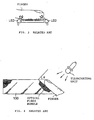
- Figs. 1 through 3 in order to meet the recent demand for reduction in size and thickness of the fingerprint input apparatus, use is made of methods illustrated in Figs. 1 through 3. Specifically, in the method illustrated in Fig. 1, light from a light source is irradiated to an end of the finger. In the method illustrated in Figs. 2A and 2B, light from LEDs (light emitting diodes) as a light source is irradiated to lateral sides of the finger. In the method illustrated in Fig. 3, light from LEDs is irradiated to the measured surface of the finger.
- LEDs light emitting diodes
- a fiber optic plate 100 comprising a bundle of a plurality of optical fibers, i.e., an optical fiber bundle, is used in order to acquire a fingerprint image.
- Each of the optical fibers has a fiber axis inclined at a specific inclination angle with respect to a normal line to a finger contact surface of the fiber optic plate 100.
- This method often adopts an optical transmissive system as a light irradiation system. Predominantly, the light is irradiated by an illuminating unit located at the opposite side opposite to the measured surface of the finger (Fig. 4) or by the light source located at the lateral sides of the finger (Figs. 2A and 2B). Rarely, use is made of the method of irradiating the light to the end of the finger as mentioned above in conjunction with Fig. 1.
- the method of using the fiber optic plate is also applicable to the optical reflective fingerprint input apparatus.
- the light from the light source is irradiated from the lateral side or obliquely from the lateral side of the finger to the optical fiber bundle of the fiber optic plate, guided to the measured surface of the finger, diffusely reflected at fingerprint valleys, and thereafter guided to the optical fiber bundle.
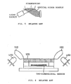
- a light transmitting ring 110 is used to position the finger.
- the light emitted from the LEDs is irradiated from a lower side or obliquely from the lower side of the ring 110 and injected through the ring 110 into the finger placed on the fiber optic plate 100.
- the light transmitted through the finger is guided through the optical fiber bundle of the fiber optic plate 100 to a two-dimensional sensor.
- the light is guided through the ring 110 as an optical guide to the finger.
- the light is irradiated to the finger from the lateral sides thereof.
- an existing fingerprint input apparatus includes a fiber optic plate 100' which comprises a combination of illuminating optical fibers for guiding light from LEDs to the finger and measuring optical fibers for guiding light transmitted through the finger to a two-dimensional sensor. As seen from Fig. 7B, the illuminating optical fibers are inclined with respect to the measuring optical fibers.
- the two-dimensional sensor is influenced by electrostatic charges accumulated in the finger. If the electrostatic charges have very strong electric energy, the two-dimensional sensor may be broken. In order to avoid the influence by the electrostatic charges, a transparent electrode layer such as tin oxide is formed on the surface of the sensor and grounded in case where the sensor is an optical sensor.
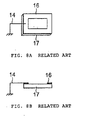
- the static capacitive sensor depicted by a reference numeral 17 is provided with an electroconductive mask 16, relatively wide, formed around a sensing or measuring surface thereof and grounded.
- a fingerprint focusing portion is reduced in thickness.
- a satisfiable technique is not yet established because of trade-off between the reduction of nonuniformity in light quantity in the measured surface and the reduction in size and thickness.
- the best approach is to irradiate the light from the opposite side of the finger opposite to the measured surface, i.e., from the side of a nail.
- this approach requires a space greater than the thickness of the finger and can not be applied to an ultraminiaturized apparatus, such as the mobile telephone, which will be widespread more and more.
- the light is irradiated obliquely from the lower side of the finger through the light transmitting ring 110 which serves as a finger position guide.
- the light is emitted from the light source (LEDs) to the air and thereafter enters into the ring 110 as the finger position guide.
- LEDs light source
- the light source must be increased in brightness. This results in an increase in power consumption.
- the light in order to compensate an insufficient light quantity without increasing the power consumption, the light must be irradiated from the close proximity of the measured surface through the ring 110 as the finger position guide. This increases the nonuniformity in light quantity in the measured surface.
- the light from the light source often enters directly into the optical fibers facing the measured surface.
- the light quantity received at a part of the finger near its base is insufficient.
- the light is irradiated directly to the measured surface of the finger.
- the illuminating optical fibers for light irradiation are arranged adjacent to the measuring optical fibers for fingerprint measurement and inclined with respect to the measuring optical fibers.
- the light from the LEDs is irradiated through the illuminating optical fibers to the finger.
- the resolution is degraded because of inclusion of the illuminating optical fibers.
- the fiber optic plate must be prepared by a combination of the illuminating optical fibers and the measuring optical fibers different in extending direction from each other. This results in an increase in production cost. Therefore, this method does not meet the demand for a low price.
- the light is irradiated to the finger obliquely from the lower side of the optical fiber bundle of the fiber optic plate.
- the illuminating optical fibers are not required.
- the light is irradiated to the measured surface of the finger through the measuring fibers (including cladding portions).
- the light scattered in an air layer at the fingerprint valley is measured as a bright part.
- this method is basically a measurement of an optical reflective type.
- external light (upon measurement during the daytime) performs a behavior of an optical transmissive type. Therefore, canceling points are present and result in unstable measurement.
- the fraction of light coming from the recessed part enters into the air layer at the valley of the fingerprint.
- the fraction of light passing through the air layer is reflected at the finger contact surface of the fiber optic plate at a reflectance which is greater as an incident angle is greater with respect to the normal line to the finger contact surface. Therefore, if the optical fiber axis is inclined to an angle at which the reflectance is great and if the fiber has a small numerical aperture, the fraction of light from the air layer hardly enters into the optical fiber.
- reflection at a boundary surface is little so that the influence is little. Therefore, the rate of incidence into the optical fiber is different between the fraction of light coming from the protruding part and the fraction of light coming from the recessed part.
- the incident angle ⁇ 1 is equal to 85° assuming that the reflectance of 50% corresponds to the critical angle. Therefore, the axis of the optical fiber must be inclined to 85°. In this event, the end face of the optical fiber has an extremely long elliptical shape. The resolution is considerably different in a long axis direction and in a short axis direction. This results in a disadvantage that the resolution in the long axis direction is degraded. Taking the above into consideration, it is necessary in practical applications to seek an optimum condition on the basis of the concept disclosed in U.S. patent No. 4,932,776.
- the measuring surface of the sensor is provided with the transparent electrode layer of a thin film, such as an ITO (Indium Tin Oxide) film.
- ITO Indium Tin Oxide
- the thin film has a large electric resistance so that a large quantity of electrostatic charges can not instantaneously be discharged.
- discharge of the electrostatic charges may deteriorate the thin film itself.
- the thin film is worn as a result of repeated contact with the finger for a long period of time so that the ability of discharging electrostatic charges is degraded.
- the static capacitive sensor 17 is provided with the electroconductive mask 16, relatively wide, formed around the measuring surface as an antistatic mask because the antistatic electrode such as the ITO film can not be applied to the surface.
- the surface of the static capacitive sensor 17 can not be protected by a relatively thick insulation film or the like. Therefore, if the finger at first comes into close proximity to the sensor before it approaches the antistatic mask, the electrostatic charges are discharged to the sensor to break the sensor.
- Fingerprint input apparatuses are as follows:
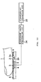
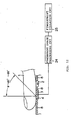
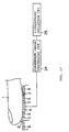
- a fingerprint input apparatus is of an optical transmissive type and comprises a fiber optic plate 3 having a finger contact surface with which a finger 1 is brought into contact in order to pick up a fingerprint image of the finger 1, and a light source 2 for emitting light.
- the light emitted from the light source 2 is at first introduced into an inside of the finger 1, is scattered within the inside of the finger 1, and comes out of the finger 1 through the surface of the finger 1 as outgoing light.
- the fingerprint image is formed.
- the light source 2 is arranged so that the light from the light source 2 enters into a substantial center of a part of the finger 1 including a first joint on a palm side and that the light source 2 is adapted to be brought into contact with the finger 1.
- the part of the finger 1 including the first joint on the palm side is a region within 10mm above and below the first joint of the finger 1 on the palm side. That is, the part including the first joint on the palm side of the finger is a region between a line nearer to a fingertip of the finger than the first joint by 10mm and a different line farther from the fingertip than the first joint by 10mm on the palm side of the finger.
- the fiber optic plate 3 comprises a bundle of a plurality of optical fibers.
- the light from the light source 2 is at first introduced into the finger 1, is scattered in the finger 1, and comes out from the surface of the finger 1 as the outgoing light.
- the outgoing light is guided through the optical fibers of the fiber optic plate 3 to a two-dimensional sensor 4. Supplied with the outgoing light, the two-dimensional image sensor 4 forms the fingerprint image.
- the fingerprint input apparatus has a measuring surface (or a finger contact surface) provided with a light shielding portion 8 formed in an area except the light source 2 and the fiber optic plate 3.
- the fingerprint image formed by the two-dimensional image sensor 4 is sent to a fingerprint image processing circuit 24. Supplied with the fingerprint image, the fingerprint image processing circuit 24 carries out predetermined image processing upon the fingerprint image to produce an image processing output signal. The fingerprint image processing circuit 24 supplies the image processing output signal to a fingerprint collation circuit 25. The fingerprint collation circuit 25 carries out fingerprint collation.
- this invention relies upon a basic technique in which the light source 2 is arranged so that the light from the light source 2 enters into the substantial center of the part of the finger 1 including the first joint on the palm side and that the light source 2 is adapted to be brought into contact with the finger 1.
- the light irradiation is carried out as follows.
- the light emitted from the light source at first enters into the air and is thereafter irradiated to the finger.
- the light emitted from the light source passes through the air, enters into the finger position guide or the like, comes out from the finger guide, and then enters into the finger. Therefore, 50 to 80% of the light quantity is lost.
- the light In order to compensate the loss, the light must be introduced into the finger from the close proximity of a measured portion. In the measured portion, the light quantity is considerably different between a center area and a peripheral area close to a position where the light is introduced. This inhibits stable and reliable measurement.
- an intermediate part at an intermediate position between the first joint of the finger 1 and the fingertip is used as the measured portion.
- the near-infrared light source 2 is located at a position corresponding to the first joint and is spaced at an appropriate distance from the measured portion. While the light advances over the above-mentioned distance, the light is scattered within the finger 1 so that the nonuniformity in light quantity is reduced. In comparison, in case where the light is irradiated from the lateral sides of the finger 1, the light quantity is nonuniform and insufficient in the center area so that the fingerprint image is dark in the center area.
- the light from the light source 2 not only irradiates a part of a measured surface near the first joint but also compensates the light quantity in the center area, which tends to be dark as mentioned above, of the measured surface up to the fingertip.
- the contrast is increased as a whole and the nonuniformity in light quantity is suppressed.
- the package 2b of the LED 2a is substantially a transparent plastic material.
- the refractive index of the plastic material is desired to be as close as possible to the refractive index (1.8) of the skin of the finger.
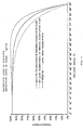
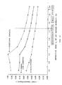
- the refractive index (P) of the LED package material is not greater than 1.5. In this event, the optical loss is suppressed to 20% or less (light transmittance being 0.80 or more), as shown in Fig.
- a fingerprint input apparatus according to an eighth embodiment of this invention utilizing the above-mentioned techniques (1) to (6).
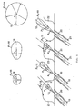
- the finger 1 is pressed along the guide 5 against the fiber optic plate 3 in which the optical fibers are arranged with their axes inclined. Simultaneously, the finger 1 is placed so that the first joint of the finger 1 to be subjected to fingerprint measurement is contacted with a near-infrared light source 10-1 (corresponding to the light source 2 in Fig. 10 etc.). At a position faced to the fingertip, a red (or green) LED 9-2 is disposed to serve as a pilot lamp and a finger position guide. With the LED 9-2 used as an indicator, the finger 1 is placed. Then, the finger 1 touches the guide (protrusion 5).
- a near-infrared light source 10-1 corresponding to the light source 2 in Fig. 10 etc.
- a red (or green) LED 9-2 is disposed to serve as a pilot lamp and a finger position guide. With the LED 9-2 used as an indicator, the finger 1 is placed. Then, the finger 1 touches the guide (protrusion 5).
- the finger 1 can be placed at a proper position. Since the near-infrared light source 10-1 has a flat upper surface, the light source 10-1 can be pressed against the first joint of the finger 1 over a wider area.
- a plurality of near-infrared light sources 10-2 for irradiating light from the lateral sides of the finger 1 are arranged at four positions in total on left and right sides.
- the light sources 10-2 irradiate near-infrared light obliquely from the lower sides to the lateral sides of the finger 1 through the finger position guide (protrusion 5) made of a light transmitting material.
- the light quantity on the left and the right sides of the measured portion is satisfied.
- the light quantity is supplemented by four red LEDs 9-1 arranged at an end portion of the measuring surface of the apparatus to serve as an indicator of the position of the finger 1 and an auxiliary light source for measurement.
- the guiding light sources 9-1 and 9-2 for producing the light for guiding the finger 1 to the proper position are disposed around the fiber optic plate 3.
- the peripheral end face of the fiber optic plate 3 is surrounded by a metal frame as the electroconductive substance 13.
- the metal frame is grounded.
- the metal frame in this embodiment has an end face flush with the surface of the fiber optic plate 3 so as to avoid an uncomfortable feeling when the finger 1 is contacted. At a first glance, it seems that the contact with the finger 1 is not sufficient. However, because the metal has an excellent conductivity and the fiber optic plate 3 has an excellent insulation, electric charges accumulated in the finger 1 are discharged towards the metal frame when the finger approaches thereto.
- the effect of this invention is as follows.
- the fiber optic plate, the two-dimensional sensor, and the finger guide are received in a thin space of about 2mm on a single plane and in an area adjacent to the measured surface of the finger.
- the fingerprint input apparatus has a compact structure and is yet resistant against the electrostatic charges and the external disturbance light.
- the small finger of a child or the like can be measured also.
- this invention is adapted to a wide range of applications.
- the optical fiber axis of the fiber optic plate used in the apparatus has an optimum inclination angle within a relatively narrow range between 45° and 60°. Therefore, the resolution in the longitudinal direction is not sacrificed.
- the finger guide in Figs. 20A and 20B is made of a transparent or a semitransparent resin and has a refractive index of about 1.4 to 1.8 which is relatively close to the refractive index of the skin of the finger.
- the light in the guide is introduced into the finger at an efficiency of 40% or more. As compared with the case where the light passes through the air, the light is more effectively used by 30% or more (Fig. 19).
- the electric power for lighting is reduced correspondingly.
- the LED arranged in the vicinity of the first joint and having a flat top surface allows smooth touch of the finger. Therefore, the apparatus can be used with comfortable feeling and the stability of measurement is not degraded.
- this invention has the following essential effect.
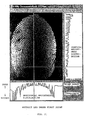
- the light source 2 in Fig. 10 (or the near-infrared light source 10-1 in Figs. 20A and 20B) is used, the fingerprint image shown in Fig. 11 is obtained..
- a fingerprint image shown in Fig. 21 is obtained.
- an illuminating method used in case of Fig. 21 will be described. Two light sources are arranged on each of the left and the right sides of the measured surface of the finger to inject light into the finger. Most of the existing illuminating methods adopt the above-mentioned arrangement.
- One example is illustrated in Figs. 2A and 2B.
- the fingerprint image is particularly dark in a lower center area.
- the lower center area seems to lose the contrast.
- the fingerprint image is read by the two-dimensional sensor.
- the longitudinal brightness distribution at the center has a contrast which is small as a whole and is further reduced towards the base of the finger.
- the transversal brightness distribution has a contrast which is not sufficient over a wide range around the center.
- the measurement is unstable. In this event, malfunction will be caused or, in the worst case, the measurement is impossible.
- the amount of calculation is considerably increased. This results in disadvantages, such as an increase in power consumption and an increase in total cost.
- the light quantity is increased in the center area in the longitudinal direction, particularly on the lower side. Therefore, the nonuniformity of contrast is reduced as a whole so that the fingerprint image shown in Fig. 11 is obtained.
- the contrast in the transversal direction is strong and uniform as a whole.
- Each of the fibers of the fiber optic plate is inclined towards the first joint of the finger. Therefore, sensitivity is high for the light from the light source 10-1. This compensates the insufficiency in light quantity in the longitudinal center area of the finger and exhibits the effect of equalizing the light quantity throughout the measured surface.
- the fiber optic plate is provided with the metal part formed throughout the entirety of the peripheral end face and grounded.
- the electrostatic charges accumulated in the finger have very strong electric energy, air discharge occurs to the metal part so as to prevent destruction of the measuring portion or disturbance of characteristics. If the finger is contacted with the metal part, the electrostatic charges are instantaneously discharged completely so as to prevent the destruction of the sensor or the malfunction due to the electrostatic charges upon measurement of the fingerprint.
- the surface of the sensor is protected by the fibers which serve as an excellent insulating material. Even if the finger touches the fibers, discharge is not directed towards the sensor but towards the metal part therearound.
- the fingerprint input apparatus of an optical transmissive type is obtained in which the light source is disposed so that the light from the light source enters into the substantial center of the part of the finger including the first joint on the palm side and that the light source is contacted with the finger.
- the fingerprint input apparatus of an optical transmissive type can be reduced in size.
Landscapes
- Engineering & Computer Science (AREA)
- Physics & Mathematics (AREA)
- Human Computer Interaction (AREA)
- General Physics & Mathematics (AREA)
- Multimedia (AREA)
- Theoretical Computer Science (AREA)
- Optics & Photonics (AREA)
- Image Input (AREA)
- Measurement Of The Respiration, Hearing Ability, Form, And Blood Characteristics Of Living Organisms (AREA)
Abstract
Description
Claims (13)
- A fingerprint input apparatus comprising a light source (2) for emitting light and a plate (3) having a finger contact surface with which a finger (1) is brought into contact in order to pick up a fingerprint image of said finger, said fingerprint image being obtained by introducing the light from said light source into an inside of the finger to scatter the light within the inside of said finger, and collecting the light coming out of said finger through a surface of said finger to form the fingerprint image, wherein:said light source is arranged so that the light from said light source enters into a substantial center of a part of said finger which part includes a first joint on a palm side of said finger and that said light source is adapted to be brought into contact with said finger.
- A fingerprint input apparatus as claimed in claim 1, wherein:said part including said first joint on the palm side of said finger is a region between a line nearer to a fingertip of said finger than said first joint by 10mm and a different line farther from said fingertip than said first joint by 10mm on the palm side of said finger.
- A fingerprint input apparatus as claimed in claim 1 or 2, wherein:said plate is a fiber optic plate (3) comprising a bundle of a plurality of optical fibers.
- A fingerprint input apparatus as claimed in claim 3, wherein:each of the optical fibers of said fiber optic plate has a fiber axis inclined towards a base of said finger at a predetermined inclination angle with respect to a normal line to the finger contact surface of said plate, the inclination angle falling within a range between 45° and 60° with respect to said normal line.
- A fingerprint input apparatus as claimed in claim 3 or 4, wherein:said fiber optic plate has a peripheral end face surrounded by an electroconductive substance (13) which is grounded.
- A fingerprint input apparatus as claimed in claim 5, wherein:the electroconductive substance is shaped to climb up onto an end portion (15) of the finger contact surface of said fiber optic plate.
- A fingerprint input apparatus as claimed in claim 5 or 6, wherein:said electroconductive substance is a light-shielding substance.
- A fingerprint input apparatus as claimed in any of claims 1 to 7, wherein:the finger contact surface of said fiber optic plate has a protruding portion (5) which serves to position said finger and which has a shape such that a fingertip of said finger is surrounded by said protruding portion except said part including said first joint, said protruding portion having a section such that one side faced to said finger extends along said finger.
- A fingerprint input apparatus as claimed in claim 8, further comprising:an additional light source (6) located in said protruding portion, said protruding portion transmitting light from said additional light source.
- A fingerprint input apparatus as claimed in claim 9, wherein:said protruding portion has a slant surface which is defined by the one side of the section faced to the finger and which is adapted to be fitted to the finger, the slant surface having a light shielding portion (7) formed in a first half region near the base of the finger, the light from said additional light source being irradiated towards the finger from a second half region of the slant surface near the fingertip of the finger.
- A fingerprint input apparatus as claimed in any of claims 1 to 10, wherein:said light source is adapted to emit near infrared light having a wavelength between 820 and 980 nm.
- A fingerprint input apparatus as claimed in any of claims 1 to 11, wherein:said light source comprises a light emitting element chip (2a) for emitting the light and a package (2b) made of a light transmitting plastic material and enveloping said light emitting element chip;said light transmitting plastic material having a refractive index not greater than 1.8 which is a refractive index of a skin of the finger.
- A fingerprint input apparatus as claimed in any of claims 1 to 12, wherein:said plate is provided with a guiding light source (9-1, 9-2) located at its periphery for emitting light to guide the finger to a proper position.
Applications Claiming Priority (2)
| Application Number | Priority Date | Filing Date | Title |
|---|---|---|---|
| JP2001331859 | 2001-10-30 | ||
| JP2001331859A JP3751872B2 (en) | 2001-10-30 | 2001-10-30 | Fingerprint input device |
Publications (3)
| Publication Number | Publication Date |
|---|---|
| EP1308876A2 true EP1308876A2 (en) | 2003-05-07 |
| EP1308876A3 EP1308876A3 (en) | 2005-01-12 |
| EP1308876B1 EP1308876B1 (en) | 2006-12-13 |
Family
ID=19147359
Family Applications (1)
| Application Number | Title | Priority Date | Filing Date |
|---|---|---|---|
| EP02024476A Expired - Lifetime EP1308876B1 (en) | 2001-10-30 | 2002-10-30 | Fingerprint input apparatus |
Country Status (11)
| Country | Link |
|---|---|
| US (1) | US6927844B2 (en) |
| EP (1) | EP1308876B1 (en) |
| JP (1) | JP3751872B2 (en) |
| KR (1) | KR100530441B1 (en) |
| CN (1) | CN100411588C (en) |
| AU (1) | AU2002301695B2 (en) |
| CA (1) | CA2410231C (en) |
| DE (1) | DE60216707T2 (en) |
| MY (1) | MY128476A (en) |
| SG (1) | SG120896A1 (en) |
| TW (1) | TWI222033B (en) |
Cited By (8)
| Publication number | Priority date | Publication date | Assignee | Title |
|---|---|---|---|---|
| EP1533759A1 (en) * | 2003-11-19 | 2005-05-25 | Ncr International Inc. | Biometric system |
| WO2008026169A1 (en) * | 2006-08-30 | 2008-03-06 | Panasonic Electric Works Co., Ltd. | Fingerprint image input apparatus |
| EP2009578A3 (en) * | 2007-06-28 | 2013-04-24 | Hitachi Ltd. | Finger vein authentication unit and information processing unit |
| WO2015054686A1 (en) | 2013-10-11 | 2015-04-16 | Lumidigm, Inc. | Miniaturized optical biometric sensing |
| EP1785937B1 (en) * | 2004-09-02 | 2015-05-06 | Sony Corporation | Information processing device |
| EP2495697A4 (en) * | 2009-10-26 | 2017-03-29 | Nec Corporation | Fake finger determination device and fake finger determination method |
| CN111095279A (en) * | 2019-07-12 | 2020-05-01 | 深圳市汇顶科技股份有限公司 | Fingerprint detection device and electronic equipment |
| EP3259702B1 (en) * | 2015-02-22 | 2023-08-02 | Microsoft Technology Licensing, LLC | Fingerprint detection with transparent cover |
Families Citing this family (71)
| Publication number | Priority date | Publication date | Assignee | Title |
|---|---|---|---|---|
| JP3150126B2 (en) | 1999-02-03 | 2001-03-26 | 静岡日本電気株式会社 | Fingerprint input device |
| US6950540B2 (en) | 2000-01-31 | 2005-09-27 | Nec Corporation | Fingerprint apparatus and method |
| JP4086523B2 (en) * | 2001-12-04 | 2008-05-14 | キヤノン株式会社 | Image reading apparatus, subject collation system, subject recognition system, and image reading method |
| US20080045788A1 (en) * | 2002-11-27 | 2008-02-21 | Zvika Gilad | Method and device of imaging with an in vivo imager |
| IL159113A (en) * | 2002-11-27 | 2008-11-26 | Given Imaging Ltd | Method and device of imaging with an imager having a fiber plate cover |
| JP3733357B2 (en) * | 2003-05-28 | 2006-01-11 | キヤノン株式会社 | Fingerprint input device and personal authentication system using the same |
| JP2005038406A (en) * | 2003-06-27 | 2005-02-10 | Canon Inc | Fingerprint input device and personal authentication system using the same |
| JP2005018594A (en) * | 2003-06-27 | 2005-01-20 | Canon Inc | Fingerprint input device, manufacturing method thereof, and personal authentication system |
| JP2005173700A (en) * | 2003-12-08 | 2005-06-30 | Canon Inc | Fingerprint reader and personal authentication system |
| JP4578109B2 (en) * | 2004-01-16 | 2010-11-10 | 三菱電機株式会社 | Fingerprint reader and fingerprint verification device |
| JP2005202877A (en) * | 2004-01-19 | 2005-07-28 | Mitsumi Electric Co Ltd | Light guide image guide member |
| FR2872318B1 (en) * | 2004-06-23 | 2006-09-22 | Sagem | OPTICAL BIOMETRIC CAPTURE DEVICE BY CONTACT AND INSTALLATION USING SUCH A DEVICE |
| US8320645B2 (en) * | 2004-11-02 | 2012-11-27 | Identix Incorporated | High performance multi-mode palmprint and fingerprint scanning device and system |
| US7265370B2 (en) * | 2005-04-28 | 2007-09-04 | Hewlett-Packard Development Company, L.P. | Sensing light |
| KR100725895B1 (en) * | 2005-09-15 | 2007-06-08 | 주식회사 아이캔텍 | Optical data input device using optical fiber |
| DE102005050807B4 (en) * | 2005-10-24 | 2010-04-08 | Dan Hossu | Device for measuring elevations and / or depressions of a surface |
| JP4599320B2 (en) * | 2006-03-13 | 2010-12-15 | 富士通株式会社 | Fingerprint authentication device, biometric finger determination device, and biometric finger determination method |
| JP2008020942A (en) | 2006-07-10 | 2008-01-31 | Rohm Co Ltd | Personal identification device and electronic device using the same |
| JP4640295B2 (en) * | 2006-09-07 | 2011-03-02 | 株式会社日立製作所 | Personal authentication apparatus and method |
| KR20080073053A (en) * | 2007-02-05 | 2008-08-08 | 주식회사 유니온커뮤니티 | Fingerprint reader with sterilization function and sterilization method |
| RU2474876C2 (en) * | 2007-09-04 | 2013-02-10 | Айдентикс Инкорпорейтед | System and high-efficiency multimode scanning device for obtaining palmprints and fingerprints |
| JP5056798B2 (en) * | 2009-06-08 | 2012-10-24 | 日本電気株式会社 | Determination device, fingerprint input device, determination method, and determination program |
| JP5023193B2 (en) * | 2010-06-28 | 2012-09-12 | 株式会社東芝 | Information processing device |
| US8437517B2 (en) | 2010-11-03 | 2013-05-07 | Lockheed Martin Corporation | Latent fingerprint detectors and fingerprint scanners therefrom |
| CN102436579B (en) * | 2011-03-31 | 2014-09-24 | 北京中控科技发展有限公司 | High-definition infrared fingerprint acquisition device |
| TWI444904B (en) * | 2011-06-24 | 2014-07-11 | Gingy Technology Inc | Finger print identification device |
| WO2013032867A1 (en) | 2011-08-26 | 2013-03-07 | Lockheed Martin Corporation | Latent fingerprint detection |
| US20130314377A1 (en) * | 2012-05-25 | 2013-11-28 | Oleg Los | Optical touch sensor apparatus |
| CN103632128A (en) * | 2012-08-24 | 2014-03-12 | 成都方程式电子有限公司 | Flat fingerprint gatherer |
| TWI518306B (en) * | 2012-10-04 | 2016-01-21 | 原相科技股份有限公司 | Image retrieving device and optical motion estimation device |
| CN103942915A (en) * | 2013-01-17 | 2014-07-23 | 鸿富锦精密工业(深圳)有限公司 | Portable alarm and alarm method thereof |
| US10356296B2 (en) | 2016-08-05 | 2019-07-16 | Gingy Technology Inc. | Light guide for finger print reader |
| TWI630502B (en) * | 2016-08-05 | 2018-07-21 | 金佶科技股份有限公司 | Image capture apparatus |
| US10049256B2 (en) | 2015-12-11 | 2018-08-14 | Gingy Technology Inc. | Fingerprint sensing module |
| US10460188B2 (en) | 2014-08-26 | 2019-10-29 | Gingy Technology Inc. | Bio-sensing apparatus |
| US10713521B2 (en) | 2016-08-05 | 2020-07-14 | Gingy Technology Inc. | Image capturing apparatus and manufacturing method thereof |
| CN105809098A (en) * | 2014-12-31 | 2016-07-27 | 上海箩箕技术有限公司 | Mobile terminal |
| US9804096B1 (en) | 2015-01-14 | 2017-10-31 | Leidos Innovations Technology, Inc. | System and method for detecting latent images on a thermal dye printer film |
| US10049257B2 (en) * | 2015-07-09 | 2018-08-14 | Gingy Technology Inc. | Fingerprint identification module |
| TWI547884B (en) * | 2015-07-09 | 2016-09-01 | 金佶科技股份有限公司 | Fingerprint identification module |
| US9818017B2 (en) | 2015-07-09 | 2017-11-14 | Gingy Technology Inc. | Fingerprint identification module |
| CN106407881B (en) * | 2015-07-29 | 2020-07-31 | 财团法人工业技术研究院 | Biometric identification device and method and wearable carrier |
| CN105095871B (en) * | 2015-07-30 | 2019-01-08 | 江苏邦融微电子有限公司 | A kind of means for anti-jamming and its method based on capacitive sensing fingerprint acquisition device |
| EP3352131B1 (en) | 2015-09-18 | 2026-04-08 | Nec Corporation | Fingerprint imaging system, fingerprint imaging method, and program |
| US11906713B2 (en) | 2015-10-14 | 2024-02-20 | Novatek Microelectronics Corp. | Optical fingerprint sensing module and display device with optical fingerprint detection |
| US10539765B2 (en) | 2015-10-14 | 2020-01-21 | Novatek Microelectronics Corp. | Optical device for fingerprint collection |
| US10177194B2 (en) | 2015-12-11 | 2019-01-08 | Gingy Technology Inc. | Fingerprint identification apparatus |
| US10198650B2 (en) | 2015-12-11 | 2019-02-05 | Gingy Technology Inc. | Image capture apparatus |
| US10056439B2 (en) | 2015-12-11 | 2018-08-21 | Gingy Technologies Inc. | Image capturing apparatus |
| TWI614694B (en) * | 2016-01-21 | 2018-02-11 | 友達光電股份有限公司 | Fingerprint sensing device |
| DE102016101607A1 (en) * | 2016-01-29 | 2017-08-03 | Bundesdruckerei Gmbh | Authentication device for authenticating a person |
| US10387710B2 (en) | 2016-03-07 | 2019-08-20 | Microsoft Technology Licensing, Llc | Image sensing with a waveguide display |
| US10043051B2 (en) | 2016-03-07 | 2018-08-07 | Microsoft Technology Licensing, Llc | Triggered image sensing with a display |
| TWI584201B (en) * | 2016-07-17 | 2017-05-21 | 金佶科技股份有限公司 | Identification apparatus and identification method |
| TWI734861B (en) * | 2016-12-19 | 2021-08-01 | 瑞典商指紋卡公司 | Capacitive fingerprint sensing device comprising display functionality |
| CN106684202B (en) * | 2017-01-04 | 2018-03-23 | 京东方科技集团股份有限公司 | A kind of photosensory assembly, fingerprint recognition panel and device |
| CN111414881B (en) * | 2017-05-12 | 2024-02-27 | Oppo广东移动通信有限公司 | Display device and mobile terminal |
| TWI664744B (en) * | 2017-06-29 | 2019-07-01 | Gingy Technology Inc. | Image capturing apparatus and manufacturing method thereof |
| CN107392181B (en) * | 2017-08-16 | 2023-06-23 | 杭州指安科技股份有限公司 | Semiconductor fingerprint module indicating device adapting to various shell structures |
| US11109797B2 (en) | 2017-09-05 | 2021-09-07 | Apple Inc. | Portable electronic device having an integrated bio-sensor |
| CN109419499B (en) * | 2017-09-05 | 2022-07-29 | 苹果公司 | Portable electronic device with integrated biosensor |
| US10515253B2 (en) * | 2017-12-27 | 2019-12-24 | Visera Technologies Company Limited | Optical fingerprint sensor |
| CN108491833B (en) * | 2018-05-22 | 2024-03-29 | 昆山丘钛生物识别科技有限公司 | Optical fingerprint module and mobile terminal |
| US10735634B2 (en) | 2018-06-14 | 2020-08-04 | Gingy Technology Inc. | Image capture apparatus |
| CN109241101B (en) * | 2018-08-31 | 2020-06-30 | 阿里巴巴集团控股有限公司 | Database query optimization method and device and computer equipment |
| KR102716356B1 (en) * | 2019-01-25 | 2024-10-10 | 삼성전자주식회사 | Texture interface for measuring biological signal and biological signal measurement apparatus comprising the same |
| CN211124078U (en) * | 2019-04-04 | 2020-07-28 | 深圳阜时科技有限公司 | Sensing module and display device |
| TWM602229U (en) * | 2019-08-16 | 2020-10-01 | 神盾股份有限公司 | Fingerprint sensing apparatus |
| US11653883B2 (en) | 2020-10-30 | 2023-05-23 | Biospectal Sa | Systems and methods for acquiring PPG signals for measuring blood pressure |
| JP7823184B2 (en) * | 2022-05-17 | 2026-03-03 | 株式会社ジャパンディスプレイ | Detection device |
| JPWO2025110058A1 (en) * | 2023-11-22 | 2025-05-30 |
Family Cites Families (25)
| Publication number | Priority date | Publication date | Assignee | Title |
|---|---|---|---|---|
| DE3707808A1 (en) | 1987-03-11 | 1988-09-22 | Sim Schilling Inter Mandata Gm | Device for recording by video the fingerprint on the end of a person's finger |
| US4932776A (en) * | 1987-11-05 | 1990-06-12 | Fingerprint Technology, Inc. | Fingerprint acquisition system |
| JPH01298473A (en) * | 1988-05-27 | 1989-12-01 | Toshiba Corp | Pattern picture processor |
| JP3045629B2 (en) * | 1993-02-17 | 2000-05-29 | 三菱電機株式会社 | Uneven pattern detector |
| JPH0762865B2 (en) * | 1993-05-13 | 1995-07-05 | 日本電気株式会社 | Fingerprint image input device |
| CN2201059Y (en) | 1994-10-25 | 1995-06-21 | 李虹 | Infrared fingerprint recognizer |
| JPH08338916A (en) | 1995-06-12 | 1996-12-24 | Hamamatsu Photonics Kk | Fiber optic plate |
| JPH0969161A (en) | 1995-06-20 | 1997-03-11 | Toshiba Corp | Personal authentication device |
| US5822445A (en) * | 1995-06-27 | 1998-10-13 | Dew Engineering And Development Limited | Apparatus for identifying fingerprints |
| JPH09134419A (en) | 1995-11-08 | 1997-05-20 | Nippon Telegr & Teleph Corp <Ntt> | Fingerprint illumination method and fingerprint imaging device |
| JP3473658B2 (en) * | 1996-07-18 | 2003-12-08 | アルプス電気株式会社 | Fingerprint reader |
| JP2927343B2 (en) * | 1996-08-05 | 1999-07-28 | 日本電気株式会社 | Fingerprint image input device and input method thereof |
| US6007782A (en) | 1996-09-11 | 1999-12-28 | Arteva North America S.A.R.L. | Reactor with a flexurally rigid stirrer element |
| JP2996295B2 (en) | 1997-02-05 | 1999-12-27 | 日本電気株式会社 | Fingerprint image input device with finger guide |
| JP2947234B2 (en) * | 1997-07-29 | 1999-09-13 | 日本電気株式会社 | Biological identification device |
| JPH11185016A (en) | 1997-12-24 | 1999-07-09 | Sharp Corp | Information processing device |
| JPH11272852A (en) | 1998-03-26 | 1999-10-08 | Sumitomo Electric Ind Ltd | Image scanner |
| US6091838A (en) * | 1998-06-08 | 2000-07-18 | E.L. Specialists, Inc. | Irradiated images described by electrical contact |
| DE19958378A1 (en) | 1999-05-16 | 2000-11-23 | Hans Juergen Poehs | Device using fingerprint for person identification, with duration and intensity of light source regulated according to ambient lighting |
| JP3150126B2 (en) | 1999-02-03 | 2001-03-26 | 静岡日本電気株式会社 | Fingerprint input device |
| JP4479024B2 (en) | 1999-10-19 | 2010-06-09 | カシオ計算機株式会社 | Imaging device |
| JP2001143056A (en) | 1999-11-16 | 2001-05-25 | Casio Comput Co Ltd | Fingerprint reader |
| US6292576B1 (en) * | 2000-02-29 | 2001-09-18 | Digital Persona, Inc. | Method and apparatus for distinguishing a human finger from a reproduction of a fingerprint |
| AU2001255172A1 (en) | 2000-03-10 | 2001-09-24 | Ethentica, Inc. | Biometric sensor |
| JP3684233B2 (en) * | 2002-05-14 | 2005-08-17 | キヤノン株式会社 | Fingerprint input device and manufacturing method thereof |
-
2001
- 2001-10-30 JP JP2001331859A patent/JP3751872B2/en not_active Expired - Lifetime
-
2002
- 2002-10-29 US US10/282,073 patent/US6927844B2/en not_active Expired - Lifetime
- 2002-10-29 CA CA002410231A patent/CA2410231C/en not_active Expired - Lifetime
- 2002-10-30 MY MYPI20024060A patent/MY128476A/en unknown
- 2002-10-30 SG SG200206599A patent/SG120896A1/en unknown
- 2002-10-30 AU AU2002301695A patent/AU2002301695B2/en not_active Expired
- 2002-10-30 CN CNB021503028A patent/CN100411588C/en not_active Expired - Lifetime
- 2002-10-30 EP EP02024476A patent/EP1308876B1/en not_active Expired - Lifetime
- 2002-10-30 DE DE60216707T patent/DE60216707T2/en not_active Expired - Lifetime
- 2002-10-30 KR KR10-2002-0066544A patent/KR100530441B1/en not_active Expired - Lifetime
- 2002-10-30 TW TW091132204A patent/TWI222033B/en not_active IP Right Cessation
Cited By (15)
| Publication number | Priority date | Publication date | Assignee | Title |
|---|---|---|---|---|
| EP1533759A1 (en) * | 2003-11-19 | 2005-05-25 | Ncr International Inc. | Biometric system |
| EP1785937B1 (en) * | 2004-09-02 | 2015-05-06 | Sony Corporation | Information processing device |
| WO2008026169A1 (en) * | 2006-08-30 | 2008-03-06 | Panasonic Electric Works Co., Ltd. | Fingerprint image input apparatus |
| EP2009578A3 (en) * | 2007-06-28 | 2013-04-24 | Hitachi Ltd. | Finger vein authentication unit and information processing unit |
| US11741744B2 (en) | 2009-10-26 | 2023-08-29 | Nec Corporation | Fake finger determination apparatus and fake finger determination method |
| EP2495697A4 (en) * | 2009-10-26 | 2017-03-29 | Nec Corporation | Fake finger determination device and fake finger determination method |
| US12633158B2 (en) | 2009-10-26 | 2026-05-19 | Nec Corporation | Fake finger determination apparatus and fake finger determination method |
| US12266210B2 (en) | 2009-10-26 | 2025-04-01 | Nec Corporation | Fake finger determination apparatus and fake finger determination method |
| EP3723034A1 (en) * | 2009-10-26 | 2020-10-14 | NEC Corporation | Fake finger determination apparatus and fake finger determination method |
| US10922525B2 (en) | 2009-10-26 | 2021-02-16 | Nec Corporation | Fake finger determination apparatus and fake finger determination method |
| WO2015054686A1 (en) | 2013-10-11 | 2015-04-16 | Lumidigm, Inc. | Miniaturized optical biometric sensing |
| EP3055693A4 (en) * | 2013-10-11 | 2017-06-21 | HID Global Corporation | Miniaturized optical biometric sensing |
| EP3259702B1 (en) * | 2015-02-22 | 2023-08-02 | Microsoft Technology Licensing, LLC | Fingerprint detection with transparent cover |
| CN111095279B (en) * | 2019-07-12 | 2023-09-08 | 深圳市汇顶科技股份有限公司 | Fingerprint detection devices and electronic equipment |
| CN111095279A (en) * | 2019-07-12 | 2020-05-01 | 深圳市汇顶科技股份有限公司 | Fingerprint detection device and electronic equipment |
Also Published As
| Publication number | Publication date |
|---|---|
| CN1493255A (en) | 2004-05-05 |
| CA2410231A1 (en) | 2003-04-30 |
| CN100411588C (en) | 2008-08-20 |
| TW200300243A (en) | 2003-05-16 |
| US20030118219A1 (en) | 2003-06-26 |
| US6927844B2 (en) | 2005-08-09 |
| EP1308876A3 (en) | 2005-01-12 |
| SG120896A1 (en) | 2006-04-26 |
| DE60216707T2 (en) | 2007-11-15 |
| KR100530441B1 (en) | 2005-11-23 |
| KR20030036051A (en) | 2003-05-09 |
| DE60216707D1 (en) | 2007-01-25 |
| EP1308876B1 (en) | 2006-12-13 |
| TWI222033B (en) | 2004-10-11 |
| JP2003141514A (en) | 2003-05-16 |
| CA2410231C (en) | 2007-07-17 |
| AU2002301695B2 (en) | 2007-03-15 |
| JP3751872B2 (en) | 2006-03-01 |
| MY128476A (en) | 2007-02-28 |
Similar Documents
| Publication | Publication Date | Title |
|---|---|---|
| EP1308876B1 (en) | Fingerprint input apparatus | |
| KR100704535B1 (en) | Fingerprint input device | |
| US10365768B2 (en) | TIR-based optical touch systems of projection-type | |
| CN211319241U (en) | Optical fingerprint detection device, touch screen and electronic equipment | |
| US7200288B2 (en) | Image reading using irradiated light | |
| TWI446223B (en) | Pointing device and electronic apparatus | |
| CN110069967A (en) | Electronic device and its taken module | |
| CN108399392B (en) | Fingerprint identification structure and display device | |
| CN112334909A (en) | Optical fingerprint detection device, touch screen and electronic equipment | |
| CN211319239U (en) | Optical fingerprint detection device, touch screen and electronic equipment | |
| CN111487708B (en) | Side-in backlight module and liquid crystal display device | |
| EP2487643A1 (en) | Relief pattern detection device | |
| WO2021146957A1 (en) | Optical fingerprint detection device, touch screen and electronic device | |
| US7119889B2 (en) | Apparatus for reducing ambient light into an optical print scanner | |
| CN112230474A (en) | Display device | |
| JP4266961B2 (en) | Fingerprint input device | |
| WO2021146955A1 (en) | Optical fingerprint detection apparatus, touch screen and electronic device | |
| JP2002117393A (en) | Fingerprint recognition sensor | |
| JP2004310574A (en) | Concavo-convex pattern detecting device, manufacturing method thereof and portable device | |
| CN210402387U (en) | Optical detection device and electronic product | |
| CN112307843B (en) | Optical detection device | |
| CN206877339U (en) | biometric identification device | |
| TWM604010U (en) | Image capturing apparatus | |
| JP2005319294A (en) | Fingerprint inputting device | |
| KR102187694B1 (en) | Optical film for fingerprinting |
Legal Events
| Date | Code | Title | Description |
|---|---|---|---|
| PUAI | Public reference made under article 153(3) epc to a published international application that has entered the european phase |
Free format text: ORIGINAL CODE: 0009012 |
|
| AK | Designated contracting states |
Designated state(s): AT BE BG CH CY CZ DE DK EE ES FI FR GB GR IE IT LI LU MC NL PT SE SK TR |
|
| AX | Request for extension of the european patent |
Extension state: AL LT LV MK RO SI |
|
| PUAL | Search report despatched |
Free format text: ORIGINAL CODE: 0009013 |
|
| AK | Designated contracting states |
Kind code of ref document: A3 Designated state(s): AT BE BG CH CY CZ DE DK EE ES FI FR GB GR IE IT LI LU MC NL PT SE SK TR |
|
| AX | Request for extension of the european patent |
Extension state: AL LT LV MK RO SI |
|
| 17P | Request for examination filed |
Effective date: 20041201 |
|
| 17Q | First examination report despatched |
Effective date: 20050613 |
|
| AKX | Designation fees paid |
Designated state(s): DE FR GB SE |
|
| GRAP | Despatch of communication of intention to grant a patent |
Free format text: ORIGINAL CODE: EPIDOSNIGR1 |
|
| GRAS | Grant fee paid |
Free format text: ORIGINAL CODE: EPIDOSNIGR3 |
|
| GRAA | (expected) grant |
Free format text: ORIGINAL CODE: 0009210 |
|
| AK | Designated contracting states |
Kind code of ref document: B1 Designated state(s): DE FR GB SE |
|
| REG | Reference to a national code |
Ref country code: GB Ref legal event code: FG4D |
|
| REF | Corresponds to: |
Ref document number: 60216707 Country of ref document: DE Date of ref document: 20070125 Kind code of ref document: P |
|
| REG | Reference to a national code |
Ref country code: SE Ref legal event code: TRGR |
|
| ET | Fr: translation filed | ||
| PLBE | No opposition filed within time limit |
Free format text: ORIGINAL CODE: 0009261 |
|
| STAA | Information on the status of an ep patent application or granted ep patent |
Free format text: STATUS: NO OPPOSITION FILED WITHIN TIME LIMIT |
|
| 26N | No opposition filed |
Effective date: 20070914 |
|
| REG | Reference to a national code |
Ref country code: FR Ref legal event code: TQ Owner name: NEC PERSONAL COMPUTERS, LTD, JP Effective date: 20111024 Ref country code: FR Ref legal event code: TQ Owner name: NEC CORPORATION, JP Effective date: 20111024 |
|
| REG | Reference to a national code |
Ref country code: GB Ref legal event code: 732E Free format text: REGISTERED BETWEEN 20111103 AND 20111109 |
|
| REG | Reference to a national code |
Ref country code: DE Ref legal event code: R082 Ref document number: 60216707 Country of ref document: DE Representative=s name: VOSSIUS & PARTNER, DE |
|
| REG | Reference to a national code |
Ref country code: DE Ref legal event code: R082 Ref document number: 60216707 Country of ref document: DE Representative=s name: VOSSIUS & PARTNER PATENTANWAELTE RECHTSANWAELT, DE Effective date: 20111221 Ref country code: DE Ref legal event code: R081 Ref document number: 60216707 Country of ref document: DE Owner name: HAMAMATSU PHOTONICS K.K., HAMAMATSU, JP Free format text: FORMER OWNER: NEC CORP., HAMAMATSU PHOTONICS K.K., , JP Effective date: 20111221 Ref country code: DE Ref legal event code: R081 Ref document number: 60216707 Country of ref document: DE Owner name: NEC PERSONAL COMPUTERS, LTD., JP Free format text: FORMER OWNER: NEC CORP., HAMAMATSU PHOTONICS K.K., , JP Effective date: 20111221 Ref country code: DE Ref legal event code: R081 Ref document number: 60216707 Country of ref document: DE Owner name: HAMAMATSU PHOTONICS K.K., HAMAMATSU, JP Free format text: FORMER OWNERS: NEC CORP., TOKYO, JP; HAMAMATSU PHOTONICS K.K., HAMAMATSU, SHIZUOKA, JP Effective date: 20111221 Ref country code: DE Ref legal event code: R081 Ref document number: 60216707 Country of ref document: DE Owner name: NEC PERSONAL COMPUTERS, LTD., JP Free format text: FORMER OWNERS: NEC CORP., TOKYO, JP; HAMAMATSU PHOTONICS K.K., HAMAMATSU, SHIZUOKA, JP Effective date: 20111221 |
|
| REG | Reference to a national code |
Ref country code: FR Ref legal event code: PLFP Year of fee payment: 15 |
|
| REG | Reference to a national code |
Ref country code: FR Ref legal event code: PLFP Year of fee payment: 16 |
|
| REG | Reference to a national code |
Ref country code: FR Ref legal event code: PLFP Year of fee payment: 17 |
|
| PGFP | Annual fee paid to national office [announced via postgrant information from national office to epo] |
Ref country code: FR Payment date: 20210913 Year of fee payment: 20 |
|
| REG | Reference to a national code |
Ref country code: DE Ref legal event code: R079 Ref document number: 60216707 Country of ref document: DE Free format text: PREVIOUS MAIN CLASS: G06K0009000000 Ipc: G06V0010000000 |
|
| PGFP | Annual fee paid to national office [announced via postgrant information from national office to epo] |
Ref country code: GB Payment date: 20210922 Year of fee payment: 20 |
|
| PGFP | Annual fee paid to national office [announced via postgrant information from national office to epo] |
Ref country code: SE Payment date: 20211012 Year of fee payment: 20 Ref country code: DE Payment date: 20210923 Year of fee payment: 20 |
|
| REG | Reference to a national code |
Ref country code: DE Ref legal event code: R071 Ref document number: 60216707 Country of ref document: DE |
|
| REG | Reference to a national code |
Ref country code: GB Ref legal event code: PE20 Expiry date: 20221029 |
|
| REG | Reference to a national code |
Ref country code: SE Ref legal event code: EUG |
|
| PG25 | Lapsed in a contracting state [announced via postgrant information from national office to epo] |
Ref country code: GB Free format text: LAPSE BECAUSE OF EXPIRATION OF PROTECTION Effective date: 20221029 |