EP1306889A2 - Electronic device with electrode and its manufacture - Google Patents
Electronic device with electrode and its manufacture Download PDFInfo
- Publication number
- EP1306889A2 EP1306889A2 EP02252255A EP02252255A EP1306889A2 EP 1306889 A2 EP1306889 A2 EP 1306889A2 EP 02252255 A EP02252255 A EP 02252255A EP 02252255 A EP02252255 A EP 02252255A EP 1306889 A2 EP1306889 A2 EP 1306889A2
- Authority
- EP
- European Patent Office
- Prior art keywords
- layer
- electronic device
- reo
- manufacturing
- mgo
- Prior art date
- Legal status (The legal status is an assumption and is not a legal conclusion. Google has not performed a legal analysis and makes no representation as to the accuracy of the status listed.)
- Granted
Links
Images


Classifications
-
- H—ELECTRICITY
- H10—SEMICONDUCTOR DEVICES; ELECTRIC SOLID-STATE DEVICES NOT OTHERWISE PROVIDED FOR
- H10B—ELECTRONIC MEMORY DEVICES
- H10B53/00—Ferroelectric RAM [FeRAM] devices comprising ferroelectric memory capacitors
-
- H—ELECTRICITY
- H10—SEMICONDUCTOR DEVICES; ELECTRIC SOLID-STATE DEVICES NOT OTHERWISE PROVIDED FOR
- H10D—INORGANIC ELECTRIC SEMICONDUCTOR DEVICES
- H10D84/00—Integrated devices formed in or on semiconductor substrates that comprise only semiconducting layers, e.g. on Si wafers or on GaAs-on-Si wafers
-
- H—ELECTRICITY
- H10—SEMICONDUCTOR DEVICES; ELECTRIC SOLID-STATE DEVICES NOT OTHERWISE PROVIDED FOR
- H10B—ELECTRONIC MEMORY DEVICES
- H10B53/00—Ferroelectric RAM [FeRAM] devices comprising ferroelectric memory capacitors
- H10B53/30—Ferroelectric RAM [FeRAM] devices comprising ferroelectric memory capacitors characterised by the memory core region
-
- H—ELECTRICITY
- H10—SEMICONDUCTOR DEVICES; ELECTRIC SOLID-STATE DEVICES NOT OTHERWISE PROVIDED FOR
- H10D—INORGANIC ELECTRIC SEMICONDUCTOR DEVICES
- H10D1/00—Resistors, capacitors or inductors
- H10D1/60—Capacitors
- H10D1/68—Capacitors having no potential barriers
- H10D1/692—Electrodes
-
- H—ELECTRICITY
- H10—SEMICONDUCTOR DEVICES; ELECTRIC SOLID-STATE DEVICES NOT OTHERWISE PROVIDED FOR
- H10D—INORGANIC ELECTRIC SEMICONDUCTOR DEVICES
- H10D1/00—Resistors, capacitors or inductors
- H10D1/60—Capacitors
- H10D1/68—Capacitors having no potential barriers
- H10D1/682—Capacitors having no potential barriers having dielectrics comprising perovskite structures
-
- H—ELECTRICITY
- H10—SEMICONDUCTOR DEVICES; ELECTRIC SOLID-STATE DEVICES NOT OTHERWISE PROVIDED FOR
- H10D—INORGANIC ELECTRIC SEMICONDUCTOR DEVICES
- H10D1/00—Resistors, capacitors or inductors
- H10D1/60—Capacitors
- H10D1/68—Capacitors having no potential barriers
- H10D1/682—Capacitors having no potential barriers having dielectrics comprising perovskite structures
- H10D1/684—Capacitors having no potential barriers having dielectrics comprising perovskite structures the dielectrics comprising multiple layers, e.g. comprising buffer layers, seed layers or gradient layers
Definitions
- the present invention relates to an electronic device having a ferroelectric layer and a method of manufacturing the same, more particularly to an electronic device having a ferroelectric layer oriented crystallographically and a method of manufacturing the same.
- a semiconductor memory in which one memory cell comprises one transistor and one capacitor, is known in the art.
- a Dynamic Random Access Memory (DRAM) capacitor contains a capacitor dielectric layer formed of a paraelectric material. Electric charges stored in the capacitor gradually decline due to discharge, even when the transistor is turned off. Accordingly, removal of an applied voltage to the memory cell causes information stored therein to decrease and disappear with time.
- DRAM Dynamic Random Access Memory
- a memory device capable of retaining information stored therein, even after power is cut off, is called a non-volatile memory.
- a non-volatile memory One known type of non-volatile memory, a one-transistor/one-capacitor type memory has a capacitor dielectric layer formed of a ferroelectric material and is termed a ferroelectric Random Access Memory (FeRAM).
- FeRAM ferroelectric Random Access Memory
- the FeRAM utilizes residual polarization of the ferroelectric material to store information therein.
- the FeRAM controls the polarity of a voltage applied between a pair of electrodes of the ferroelectric capacitor, thus controlling the direction of the residual polarization. Assuming that one polarization direction be "1" and the other be "0", binary information can be stored. Since the residual polarization remains in the ferroelectric capacitor, even after the applied voltage is removed therefrom, the non-volatile memory can be re-accessed.
- the non-volatile memory enables information to be rewritten a large number of times, i.e. 10 10 to 10 12 times.
- the non-volatile memory also has a rewriting speed of an order of several tens of nanoseconds and offers a high-speed operability.
- Ferroelectric materials such as lead-based oxide ferroelectric materials having a perovskite structure and bismuth-based oxide ferroelectric materials having a bismuth-layered structure are known.
- Typical examples of the lead-based ferroelectric materials are PbZr x Ti 1-x O 3 (PZT), Pb y La 1-y Zr x Ti 1-x O 3 (PLZT) and the like.
- a typical example of the bismuth-based oxide ferroelectric materials is SrBi 2 Ta 2 O 9 (BST) .
- the ferroelectric capacitor offers a higher charge retention capability as the polarization of the ferroelectric material is greater, and can retain the electric potential with less capacitance.
- the FeRAM may be fabricated with high integration. Furthermore, as the level of polarization of the ferroelectric material is greater, the polarization directions can be differentiated more clearly even at a low reading-out voltage, thus enabling the ferroelectric memory to be driven at a low voltage.
- the Journal of Applied Physics 1991, vol. 70, No. 1 on pages 382 to 388 discloses a method of obtaining a (111)-oriented ferroelectric thin film, in which metal thin films, formed of metals such as platinum (Pt) and iridium (Ir), are deposited at 500°C to obtain a (111)-oriented metal thin film, and a ferroelectric thin film, such as PZT, is deposited thereon at room temperature, followed by heating of the deposited ferroelectric thin film to a range from 650°C to 700°C.
- the maximum temperature permitted for a manufacturing process of the FeRAM is usually 620°C.
- a ferroelectric material such as PZT, having simple tetragonal perovskite structure, a polarization axis along the c axis, ⁇ 100> direction. Accordingly, the polarization amount is at a maximum when the ferroelectric layer is oriented approximately along a (001) plane (hereinafter, referred to as (001)-oriented).
- (001)-oriented a component of the polarization produced in the ⁇ 100> direction is only about 1/1.73 of that in ⁇ 111> direction, the thickness direction of the ferroelectric layer.
- the polarization can be increased by aligning orientation, it is impossible to increase the polarization to the maximum.
- An object of the present invention is to provide an electronic device with a ferroelectric layer having a large degree of polarization and a method of manufacturing the same.
- an electronic device including: an ReO 3 layer having a (001) orientation; and an oxide ferroelectric layer having a perovskite structure, the oxide ferroelectric layer being formed on the ReO 3 layer and having a (001) orientation.
- a method of manufacturing an electronic device including the sequential steps of: preparing a ReO 3 layer and having a (001) orientation; and forming an oxide ferroelectric layer having a perovskite structure on the ReO 3 layer, the oxide ferroelectric layer having a (001) orientation.
- a (001)-oriented MgO layer is preferably used as a layer underlying the ReO 3 layer.
- Lattice matching can be made for the (001)-oriented ReO 3 layer and the (001)-oriented oxide ferroelectric layer having a perovskite structure; accordingly, the (001)-oriented oxide ferroelectric layer having a perovskite structure can be formed on the (001)-oriented ReO 3 layer.
- the MgO layer can be (001)-oriented with ease. Lattice matching can be made for both the (001)-oriented MgO layer and the (001)-oriented ReO 3 layer. Hence, the (001)-oriented ReO 3 layer and the (001)-oriented oxide ferroelectric layer having a perovskite structure can be formed sequentially on the (001)-oriented MgO layer.
- ReO 3 used herein includes ReO 3 to which metal other than Re is added, for example, for controlling a lattice constant thereof.
- Fig. 1A shows the structure of a ferroelectric capacitor according to a first embodiment of the present invention.
- a silicon oxide layer 11 is formed on an Si substrate 10.
- the silicon oxide layer 11 may be formed, for example, by thermal oxidation of silicon or Chemical Vapour Deposition (CVD).
- the silicon oxide layer 11 is of an amorphous character.
- a (001)-oriented MgO layer 12 is formed on the silicon oxide layer 11, a (001)-orientated ReO 3 layer 13 is formed on the MgO layer 12, a (001)-oriented PZT layer 14 is formed on the ReO 3 layer 13. All the aforesaid layers 12, 13 and 14 can be deposited by Organometallic Chemical Vapour Deposition (OMCVD) using an organometallic material.
- OMCVD Organometallic Chemical Vapour Deposition
- Fig. 1B schematicaly shows an arrangement of an apparatus for depositing a film by OMCVD.
- a liquid container 21-1 contains a solution of the organometallic material to be deposited. Pressurized He gas is fed to the liquid container 21-1 via a pipe terminating above the solution.
- a second pipe 22-1 has an end portion immersed in the solution to allow the solution to flow into the container 21-1.
- the flow rate of the supplied solution is controlled by a Mass Flow Controller (MFC) 24-1, and the solution is supplied to a vapourizer 27-1 through a pipe 25-1.
- MFC Mass Flow Controller
- a carrier gas pipe 26 is connected to the vapourizer 27-1.
- the raw material liquid supplied to the vapourizer 27-1 together with carrier gas N 2 is vapourized by the vapourizer 27-1 and supplied to a pipe 28-1.
- a liquid container 21-2, a pipe 22-2, a mass flow controller 24-2, a pipe 25-2, a vapourizer 27-2 and a pipe 28-2 have similar structures as those of the liquid container 21-1, the pipe 22-1, the mass flow controller 24-1, the pipe 25-1, the vapourizer 27-1 and the pipe 28-1 respectively, as hereinbefore described. Furthermore, any number of similar raw material supply systems may be provided.
- the vapourizer 27-1 may be connected with other liquid systems containing raw material and which may have similar structure as those of the liquid container 21-1, the pipe 22-1, the Mass Flow Controller 24-1 and the pipe 25-1.
- Other vapourizers may also be provided with any number of the raw liquid material supply systems.
- a reaction chamber 30 has raw material pipes such as a gas pipe 29 and the raw liquid material pipes 28-1, 28-2..., and can supply raw material gas from a showerhead 32.
- a susceptor 34 capable fo controlling the temperature is disposed at a lower portion of the reaction chamber 30.
- a substrate 35 composed of, for example, a silicon base layer provided with a silicon oxide layer is disposed on the susceptor 34.
- the above described embodiment is not limited to multiple supply systems and a single system may be employed. Furthermore, a plurality of the reaction chambers may also be provided.
- a solution may be obtained by dissolving Mg(DPM) 2 where DPM is dipivaloilmethanate) in tetrahydrofuran (THF).
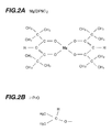
- Fig. 2A is a chemical formula showing the chemical structure of Mg(DPM) 2 .
- Dipivaloilmethanate (DPM) is bonded through an oxygen atom at each side of an Mg atom.
- DPM is monovalent but forms a coordinate bond via its carbonyl group to form a chelate with the Mg atom.
- n DPM's may be bonded to an n valent atom, so that in this case for every one Mg, there are two DPMs bonded thereto. If an Re material is used, then a solution may be obtained by dissolving Re(DPM) 2 in THF.
- the chemical structure of Re(DPM) 2 is equivalent to that of Mg(DPM) 2 as shown in Fig. 2A.
- Pb(DPM) 2 a solution may then be obtained by dissolving Pb(DPM) 2 in THF.
- the structure of Pb(DPM) 2 is equivalent to that of Mg(DPM) 2 as shown in Fig. 2A.
- a solution may be obtained by dissolving Zr(DPM) 4 in THF Zr(DPM) 4 has a different structure to that of the aforementioned chelates, whereby four DPMs are bonded around one Zr atom.
- a solution may be obtained by dissolving Ti (i-PrO) 2 (DPM) 2 (where i-PrO is an iso-proxy group)in THF.
- the structure of Ti (i-PrO) 2 (DPM) 2 is equivalent to that of Mg(DPM) 2 as shown in Fig. 2A, but also binds with two iso-proxy groups, as shown in Fig. 2B, to Ti.
- the organometallic material is not limited to these examples.
- pressurized helium (He) gas is fed to the liquid containers 21 in which the solution obtained by dissolving Mg(DPM) 2 in THF is contained.
- the solution is vapourised by passing it through the vapourizers 27 at 260°C, and loaded into the carrier gas N 2 .
- the Mg raw material is fed through the pipes 28 to the showerhead 32 by means of an N 2 carrier gas, and carried over the silicon oxide film of the substrate 35 together with O 2 gas supplied from the pipe 29.
- the silicon oxide film is then heated to 560°C, whereby it decomposes the organometallic gas present.
- the decomposed gas combines with the oxygen, thus precipitating MgO and forming a (001)-oriented MgO layer deposited on the silicon oxide film.
- the thickness of the (001)-oriented MgO layer is set, for example, in a range from 50 to 100 nm.
- the temperature is not limited to 560°C.
- decomposition of the organometallic gas is carried out with a substrate temperature of 620°C or below, which may enable temperature compatibilities with other manufacturing steps for the production of the FeRAM device.
- the liquid raw material obtainable by dissolving Re(DPM) 2 in THF, which is contained in the liquid containers 21, is fed to the showerhead 32 by means of a carrier gas in the same manner as the process hereinbefore described.
- the showerhead 32 is supplied with O 2 gas, mixed gas of O 2 gas and N 2 gas or the like.
- Other mixed O 2 gases may include O 2 /Ar, O 2 /He and O 2 /N 2 O.
- the substrate 35 having the (001)-oriented MgO layer 12 formed thereon is kept at a constant temperature of 560°C by means of the susceptor 34.
- the raw material gas is supplied to the heated (001)-oriented MgO layer 12 whereby a (001)-oriented ReO 3 layer 13 is deposited thereon.
- the thickness of the (001)-oriented ReO 3 layer may be set, for example, in a range from 20 to 50 nm.
- the PZT layer 14 is deposited thereon.
- the Pb solution is obtained by dissolving Pb(DPM) 2 in THF
- the Zr solution is obtained by dissolving Zr(DPM) 4 in THF
- the Ti solution is obtained by dissolving Ti (i-PrO) 2 (DPM) 2 in THF.
- Pressurized helium gas is fed into three liquid containers containing these liquid raw materials, and the liquid raw materials are vapourized by one or three vapourizers and supplied to the showerhead 32.
- the substrate temperature is kept at 560°C, and gaseous Pb(DPM) 2 , Zr(DPM) 4 and Ti(i-PrO) 2 (DPM) 2 together with oxygen are simultaneously blown over the substrate, as a result of which the Pb(Zr, Ti)O 3 (PZT) layer 14 is deposited on the (001)-oriented ReO 3 layer 13.
- the deposited PZT layer 14 also has (001) orientation.
- the thickness of the (001)-oriented PZT layer 14 may be set, for example, in a range from 80 to 150 nm.
- ferroelectric oxide materials having a perovskite structure may also be employed.
- Pb y La 1-y Zr x Ti 1-x O 3 (PLZT) Pb 1-a-b-c La a Sr b Ca c Zr 1-x Ti x O 3 (PLSCZT) and the like can be used.
- an MgO layer is deposited on an amorphous silicon oxide layer 11 by OMCVD, in order to obtain a (001)-oriented MgO layer 12.
- a ReO 3 layer 13 which is (001)-oriented in accordance with the orientation of the underlying layer, that is, the MgO layer 12.
- the PZT layer 14 can be deposited on the (001)-oriented ReO 3 layer 13, the PZT layer 14 being (001)-oriented in accordance with the orientation of the underlying layers, that is, the MgO layer 12 and the ReO 3 layers 13.
- An upper electrode 15 is formed on the PZT layer 14.
- the upper electrode 15 is not required to be (001)-oriented and can be formed one of various known electrode materials irrespective of the orientation of the ferroelectric layer.
- an IrO 2 layer may be deposited by OMCVD, in which case an Ir solution obtained by dissolving Ir(DPM) 3 in THF is used.
- the process for vapourizing the material is similar as that as hereinbefore described.
- the substrate temperature is kept at 560°C, and, e.g. Ir(DPM) 3 gas, and oxygen are simultaneously blown thereover, thus enabling the upper IrO 2 electrode 15 or IrO 2 layer to be deposited on the PZT layer 14.
- the thickness of the IrO 2 layer 15 may be set, for example, in a range from 100 to 150 nm.
- a stacked layer 15 obtained by stacking an IrO 2 layer 15-1 and a SrRuO 3 layer 15-2 may be used.
- Deposition methods other than OMCVD may also be used.
- the IrO 2 layer 15-1 can be deposited by sputtering using an IrO 2 target.
- the substrate is kept at a room temperature, and the target is sputtered by use of Ar gas under a vacuum of 3x10 -4 Torr.
- the thickness of the IrO 2 layer 15-1 may be set, for example, in a range from 100 to 150 nm.
- the SrRuO 3 layer 15-2 being deposited on the IrO 2 layer 15-1, can also be deposited by sputtering.
- SrRuO 3 is used as a target, the substrate is kept at a room temperature, the vacuum is set at 3x10 -4 Torr under Ar gas. Under the above-described conditions, the target is sputtered, and thus the SrRuO 3 layer 15-2 is deposited.
- the thickness of the SrRuO 3 layer 15-2 may be set, for example, in a range from 10 to 30 nm.
- a metal layer used as an electrode may be utilized effectively as long as an electrical resistivity thereof is 10 -5 ⁇ m or less.
- ReO 3 in the presence of a small amount of another metal shows an electrical resistance of an order of 10 -6 ⁇ m at 300°K. Accordingly, ReO 3 , with other metal impurities can still be utilized effectively as such an electrode of the ferroelectric capacitor.
- the MgO layer is deposited on the amorphous silicon oxide layer 11, thus forming the (001)-oriented MgO layer 12; however, it will be obvious that a (001) plane of single crystal MgO can be used in place of the deposited MgO layer.
- Fig. 1D shows the case where a ReO 3 layer 13 and a ferroelectric layer 14 having a perovskite structure, are epitaxially grown in this order on a single crystal MgO layer 12 having a (001) plane, an upper electrode 15 being formed on the ferroelectric layer 14.
- the ferroelectric layer 14 is (001)-oriented, thus enabling the polarization caused by an applied voltage to be aligned to a direction perpendicular to the electrode surface, thus utilising the polarization of the ferroelectric layer in an efficient manner.
- Figs. 3A and 3B show examples of arrangements of electronic devices, each using the ferroelectric capacitor as hereinbefore described.
- Fig.3A shows an example where electrodes (extension electrodes hereinafter) extend out of upper and lower surfaces of a ferroelectric capacitor.
- An element isolation region 40 is formed on a surface of an Si substrate 10 by Shallow Trench Isolation (STI).
- STI Shallow Trench Isolation
- MOS Metal-Oxide-Semiconductor
- the two MOS transistors have one common source/drain region 46 and other separate source/drain regions 45 on both sides which are connected with the ferroelectric capacitors, respectively.
- An insulated gate electrode formed of a gate insulating film 41, a polycrystalline gate electrode 42 and a silicide gate electrode 43 are disposed along connecting channels between the source/drain regions.
- a side spacer 44 is formed on a sidewall of the insulated gate electrode 43.
- An amorphous insulating layer 11 made of silicon oxide or the like is formed over surfaces where the semiconductor devices are located. Furthermore, a (001)-oriented MgO layer 12 is formed on a surface of the amorphous insulating layer 11.
- a contact hole is formed through the MgO layer 12 and through the amorphous insulating layer 11.
- An extraction plug composed of, for example, a barrier metal 48 and a tungsten (W) plug 49 is formed in the contact hole. Then, the electrode layers on the MgO layer 12 which are no longer required, are removed by, for example, Chemical Mechanical Polishing (CMP).
- CMP Chemical Mechanical Polishing
- a ferroelectric capacitor composed of the lower ReO 3 layer 13, the ferroelectric layer 14 having a perovskite structure 14 and finally, the upper electrode 15.
- the MgO layer 12 is (001)-oriented, thus making it possible to form the (001)-oriented lower ReO 3 layer 13 and the (001)-oriented ferroelectric layer 14 having a perovskite structure.
- an insulating layer 50 made of silicon oxide or the like is deposited to cover the outer surface thereof.
- a contact hole is formed through the insulating layer 50, and then a barrier metal layer 51 and a metal conductive layer 52 made of W or the like are buried therein, thus the extraction electrode is formed.
- unnecessary electrode layers on the insulating layer 50 are removed, and upper wirings 54 and 55 are formed. Surfaces of the upper wirings 54 and 55 are covered with an insulating layer 60.
- Fig. 3B shows an arrangement, in which two electrodes extend out of the upper surface of the ferroelectric capacitor.
- An element isolation region 40 of silicon oxide film is formed on the surface of the Si substrate 10 by the local oxidation of silicon.
- One MOS transistor is formed in an active region defined by the element isolation region 40.
- An insulated gate electrode formed of a gate insulating film 41, a polycrystalline gate electrode 42 and a polycrystalline silicide gate electrode 43 are disposed in a channel region of the arrangement.
- a side spacer 44 is formed on a sidewall of the insulated gate electrode.
- Source/drain regions 45 and 46 are formed on both sides of the gate electrode by ion implantation and the like.
- An amorphous insulating layer 48 made of silicon oxide or the like is formed to cover the MOS transistor. Plugs 49 for providing the source/drain regions 45 and 46 are formed.
- a layer 59, for example silicon nitride, having an amorphous phase is formed on a surface of the amorphous insulating layer 48 through which the plugs 49 project, thus forming an oxygen shielding layer.
- a (001)-oriented MgO layer 12 is formed on the amorphous silicon nitride layer 59. It is conceivable that the (001)-oriented MgO layer 12 may only be deposited upon an underlying amorphous layer.
- a ferroelectric capacitor composed of a (001)-oriented ReO 3 layer 13, a (001)-oriented ferroelectric layer 14 having a perovskite structure and an upper electrode 15 are formed on the (001)-oriented MgO layer 12.
- the lower ReO 3 electrode 13 is extrapolated along a direction perpendicular to the electrode surface.
- An insulating layer 18 made of silicon oxide or the like is formed to cover the ferroelectric capacitor.
- Desired portions of the insulating layer 18, MgO layer 12 and silicon nitride layer 59 are removed by etching, to form contact holes, in which wiring 19 connects the plug 49 exposed in the contact hole with the upper electrode 15.
- An insulating layer 50 is further formed to cover the local wiring 19. Through the insulating layer 50, a second opening for exposing the plug 49 on the source/drain region 46 is formed into which a second wiring 55 is arranged.
- Multi-layered wiring structures can be formed by other publicly known techniques.
- an electronic device for example, a semiconductor integrated circuit device can be manufactured with the ferroelectric capacitor.
Landscapes
- Semiconductor Memories (AREA)
- Ceramic Capacitors (AREA)
- Chemical Vapour Deposition (AREA)
- Formation Of Insulating Films (AREA)
Abstract
Description
Specifically, the FeRAM may be fabricated with high integration. Furthermore, as the level of polarization of the ferroelectric material is greater, the polarization directions can be differentiated more clearly even at a low reading-out voltage, thus enabling the ferroelectric memory to be driven at a low voltage.
Accordingly, ReO3, with other metal impurities can still be utilized effectively as such an electrode of the ferroelectric capacitor.
A
After forming the extraction electrode, unnecessary electrode layers on the insulating
Claims (22)
- An electronic device comprising:a ReO3 layer having a (001) orientation; andan oxide ferroelectric layer having a perovskite structure, said oxide ferroelectric layer being formed on said ReO3 layer and having a (001) orientation.
- The electronic device according to claim 1, further comprising: a MgO layer having a (001) orientation, wherein said ReO3 layer is formed on said MgO layer.
- The electronic device according to claim 2 further comprising: an amorphous layer, wherein said MgO layer is formed on said amorphous layer.
- The electronic device according to any one of claims 1-3 further comprising: an upper electrode formed on said oxide ferroelectric layer.
- The electronic device according to claim 3 or 4, wherein said amorphous layer forms an insulating layer, wherein said amorphous layer encapsulates a semiconductor element formed on a semiconductor substrate and a conductive plug is provided to electrically connect said semiconductor element, said conductive plug penetrating through said insulating layer.
- The electronic device according to claim 5 wherein a ReO3 layer is formed on said insulating layer so as to be over said conductive plug.
- The electronic device according to claim 6, further comprising:a second insulating layer covering said upper electrode;a plurality of apertures penetrating through said second insulating layer and exposing said conductive plug and said upper electrode; andsaid conductive plug and said upper electrode being connected via said apertures by means of local wiring.
- The electronic device according to any one of claims 2-7, wherein said MgO layer is a single crystal MgO layer having a (001) plane.
- The electronic device according to any preceding claim, wherein said ReO3 layer is added with metal other than Re.
- The electronic device according to any one of claims 4-9 wherein said upper electrode is formed of an IrO2 layer, or a stack of an IrO2 layer and a SrRuO3 layer.
- The electronic device according to any preceding claim wherein ferroelectric layer is PZT.
- The electronic device according to any one of claims 5-11 wherein said conductive plug is tungsten.
- A method of manufacturing an electronic device, comprising the sequential steps of:(a) preparing an ReO3 layer having a (001) orientation; and(b) forming an oxide ferroelectric layer having a perovskite structure and a (001) orientation, on said ReO3 layer.
- The method of manufacturing an electronic device according to claim 13, wherein said step (a) includes the sequential steps of:(a-1) preparing a MgO layer having a (001) orientation; and(a-2) forming said ReO3 layer having a (001) orientation on said MgO layer.
- The method of manufacturing an electronic device according to claim 13, wherein said ReO3 layer is deposited on a single crystal MgO layer having (001) orientation.
- The method of manufacturing an electronic device according to claim 14, wherein said step (a-1) includes the sequential steps of:(a-1-1) preparing an amorphous layer; and(a-1-2) forming said MgO layer having a (001) orientation on said amorphous layer.
- The method of manufacturing an electronic device according to claim 16, wherein at least one of said steps (a-1-2), (a-2) and (b) is executed by Organometallic Chemical Vapour Deposition (OMCVD).
- The method of manufacturing an electronic device according to claim 16, wherein all of said steps (a-1-2), (a-2) and (b) are executed by OMCVD.
- The method of manufacturing an electronic device according to claim 17 or 18, wherein said OMCVD is executed at a substrate temperature of 620°C or lower.
- The method of manufacturing an electronic device according to one of claims 17-19, wherein an organometallic raw material for use in said OMCVD comprises a dipivaloilmethanate (DPM) - metal chelate or an iso-proxy (i-PrO) bound metal.
- The method of manufacturing an electronic device according to claim 16, wherein at least one of said steps (a-1-2), (a-2) and (b) is executed by sputtering.
- The method of manufacturing an electronic device according to any one of claims 13-21, further comprising the step of : (c) forming at least one upper electrode layer on said oxide ferroelectric layer.
Applications Claiming Priority (2)
| Application Number | Priority Date | Filing Date | Title |
|---|---|---|---|
| JP2001329688A JP2003133531A (en) | 2001-10-26 | 2001-10-26 | Electronic device and manufacturing method thereof |
| JP2001329688 | 2001-10-26 |
Publications (3)
| Publication Number | Publication Date |
|---|---|
| EP1306889A2 true EP1306889A2 (en) | 2003-05-02 |
| EP1306889A3 EP1306889A3 (en) | 2004-08-18 |
| EP1306889B1 EP1306889B1 (en) | 2007-01-17 |
Family
ID=19145544
Family Applications (1)
| Application Number | Title | Priority Date | Filing Date |
|---|---|---|---|
| EP02252255A Expired - Lifetime EP1306889B1 (en) | 2001-10-26 | 2002-03-27 | Electronic device with electrode and its manufacture |
Country Status (7)
| Country | Link |
|---|---|
| US (2) | US6744085B2 (en) |
| EP (1) | EP1306889B1 (en) |
| JP (1) | JP2003133531A (en) |
| KR (1) | KR20030035761A (en) |
| CN (1) | CN1212665C (en) |
| DE (1) | DE60217610T2 (en) |
| TW (1) | TW535179B (en) |
Families Citing this family (28)
| Publication number | Priority date | Publication date | Assignee | Title |
|---|---|---|---|---|
| US7494927B2 (en) * | 2000-05-15 | 2009-02-24 | Asm International N.V. | Method of growing electrical conductors |
| JP2004356313A (en) * | 2003-05-28 | 2004-12-16 | Seiko Epson Corp | Semiconductor device and manufacturing method thereof |
| CN100420024C (en) * | 2003-06-06 | 2008-09-17 | 富士通株式会社 | Manufacturing method of semiconductor device |
| JP4082711B2 (en) | 2004-03-12 | 2008-04-30 | 独立行政法人科学技術振興機構 | Magnetoresistive element and manufacturing method thereof |
| JP2006073648A (en) | 2004-08-31 | 2006-03-16 | Fujitsu Ltd | Semiconductor device and manufacturing method thereof |
| US8025922B2 (en) | 2005-03-15 | 2011-09-27 | Asm International N.V. | Enhanced deposition of noble metals |
| US7666773B2 (en) | 2005-03-15 | 2010-02-23 | Asm International N.V. | Selective deposition of noble metal thin films |
| KR100725081B1 (en) * | 2005-06-14 | 2007-06-08 | 후지쯔 가부시끼가이샤 | Manufacturing Method of Semiconductor Device |
| US20070014919A1 (en) * | 2005-07-15 | 2007-01-18 | Jani Hamalainen | Atomic layer deposition of noble metal oxides |
| JP5211558B2 (en) * | 2007-06-18 | 2013-06-12 | 富士通セミコンダクター株式会社 | Manufacturing method of semiconductor device |
| US20090087339A1 (en) * | 2007-09-28 | 2009-04-02 | Asm Japan K.K. | METHOD FOR FORMING RUTHENIUM COMPLEX FILM USING Beta-DIKETONE-COORDINATED RUTHENIUM PRECURSOR |
| JP4888418B2 (en) * | 2008-02-29 | 2012-02-29 | ソニー株式会社 | Variable capacitance element and control method thereof, electronic device, and communication mobile device |
| WO2009122497A1 (en) | 2008-03-31 | 2009-10-08 | 富士通マイクロエレクトロニクス株式会社 | Ferroelectric memory and its manufacturing method, and ferroelectric capacitor manufacturing method |
| US8084104B2 (en) * | 2008-08-29 | 2011-12-27 | Asm Japan K.K. | Atomic composition controlled ruthenium alloy film formed by plasma-enhanced atomic layer deposition |
| US8133555B2 (en) | 2008-10-14 | 2012-03-13 | Asm Japan K.K. | Method for forming metal film by ALD using beta-diketone metal complex |
| US9379011B2 (en) | 2008-12-19 | 2016-06-28 | Asm International N.V. | Methods for depositing nickel films and for making nickel silicide and nickel germanide |
| US20110020546A1 (en) * | 2009-05-15 | 2011-01-27 | Asm International N.V. | Low Temperature ALD of Noble Metals |
| KR200458200Y1 (en) * | 2010-04-06 | 2012-01-30 | 오길식 | Cover floating LED ceiling that is hard to disassemble |
| CN102151526A (en) * | 2010-07-23 | 2011-08-17 | 兰州理工大学 | Method for regulating iron magnetic transition temperature of perovskite magnanite |
| US8871617B2 (en) | 2011-04-22 | 2014-10-28 | Asm Ip Holding B.V. | Deposition and reduction of mixed metal oxide thin films |
| US8866367B2 (en) | 2011-10-17 | 2014-10-21 | The United States Of America As Represented By The Secretary Of The Army | Thermally oxidized seed layers for the production of {001} textured electrodes and PZT devices and method of making |
| US9761785B2 (en) | 2011-10-17 | 2017-09-12 | The United States Of America As Represented By The Secretary Of The Army | Stylo-epitaxial piezoelectric and ferroelectric devices and method of manufacturing |
| US9607842B1 (en) | 2015-10-02 | 2017-03-28 | Asm Ip Holding B.V. | Methods of forming metal silicides |
| US9876018B2 (en) * | 2015-12-03 | 2018-01-23 | Micron Technology, Inc. | Ferroelectric capacitor, ferroelectric field effect transistor, and method used in forming an electronic component comprising conductive material and ferroelectric material |
| US10896950B2 (en) * | 2017-02-27 | 2021-01-19 | Nxp Usa, Inc. | Method and apparatus for a thin film dielectric stack |
| US10923286B2 (en) | 2018-02-21 | 2021-02-16 | Nxp Usa, Inc. | Method and apparatus for compensating for high thermal expansion coefficient mismatch of a stacked device |
| KR102953798B1 (en) | 2020-06-24 | 2026-04-15 | 에이에스엠 아이피 홀딩 비.브이. | Vapor deposition of films comprising molybdenum |
| CN115959905B (en) * | 2022-12-07 | 2023-08-18 | 南京航空航天大学 | A kind of lead zirconate titanate and magnesium oxide vertical self-assembled nanocomposite dielectric energy storage film and its preparation method |
Family Cites Families (16)
| Publication number | Priority date | Publication date | Assignee | Title |
|---|---|---|---|---|
| US5192723A (en) * | 1990-09-04 | 1993-03-09 | Nikon Corporation | Method of phase transition, method for producing lead niobate-based complex oxide utilizing said phase transition method, and lead niobate-based complex oxide produced by said method |
| DE69326944T2 (en) * | 1992-04-13 | 2000-03-30 | Sharp Kk | STACK ELECTRODES FOR FERROELECTRICAL DEVICES |
| US5514484A (en) * | 1992-11-05 | 1996-05-07 | Fuji Xerox Co., Ltd. | Oriented ferroelectric thin film |
| JPH07153643A (en) | 1993-11-29 | 1995-06-16 | Nissin Electric Co Ltd | Laminated dielectric device |
| JP3460095B2 (en) * | 1994-06-01 | 2003-10-27 | 富士通株式会社 | Ferroelectric memory |
| DE4421007A1 (en) * | 1994-06-18 | 1995-12-21 | Philips Patentverwaltung | Electronic component and method for its production |
| JPH098243A (en) | 1995-06-20 | 1997-01-10 | Matsushita Electron Corp | Joining structure of metallic electrode to ceramic thin film, semiconductor device, and its manufacture |
| KR100199095B1 (en) * | 1995-12-27 | 1999-06-15 | 구본준 | Capacitor Structure of Semiconductor Memory Cell and Manufacturing Method Thereof |
| JP3435966B2 (en) * | 1996-03-13 | 2003-08-11 | 株式会社日立製作所 | Ferroelectric element and method of manufacturing the same |
| US6548342B1 (en) * | 1996-08-20 | 2003-04-15 | Hitachi, Ltd. | Method of producing oxide dielectric element, and memory and semiconductor device using the element |
| JPH10189887A (en) * | 1996-12-27 | 1998-07-21 | Sanyo Electric Co Ltd | Electorde for ferroelectric body and ferroelectric device using the same |
| JP3974697B2 (en) * | 1997-11-28 | 2007-09-12 | ローム株式会社 | Capacitor and its manufacturing method |
| US6432793B1 (en) * | 1997-12-12 | 2002-08-13 | Micron Technology, Inc. | Oxidative conditioning method for metal oxide layer and applications thereof |
| US6117689A (en) * | 1997-12-24 | 2000-09-12 | Texas Instruments Incorporated | Stable high-dielectric-constant material electrode and method |
| US6258459B1 (en) * | 1998-04-28 | 2001-07-10 | Tdk Corporation | Multilayer thin film |
| US6815219B2 (en) * | 1999-12-27 | 2004-11-09 | Hynix Semiconductor Inc. | Fabrication method and structure for ferroelectric nonvolatile memory field effect transistor |
-
2001
- 2001-10-26 JP JP2001329688A patent/JP2003133531A/en active Pending
-
2002
- 2002-02-19 US US10/076,349 patent/US6744085B2/en not_active Expired - Fee Related
- 2002-03-05 TW TW091104016A patent/TW535179B/en not_active IP Right Cessation
- 2002-03-15 KR KR1020020014011A patent/KR20030035761A/en not_active Abandoned
- 2002-03-27 EP EP02252255A patent/EP1306889B1/en not_active Expired - Lifetime
- 2002-03-27 DE DE60217610T patent/DE60217610T2/en not_active Expired - Fee Related
- 2002-03-28 CN CNB021083045A patent/CN1212665C/en not_active Expired - Fee Related
-
2004
- 2004-04-12 US US10/821,841 patent/US7153705B2/en not_active Expired - Fee Related
Also Published As
| Publication number | Publication date |
|---|---|
| US20040195605A1 (en) | 2004-10-07 |
| US7153705B2 (en) | 2006-12-26 |
| JP2003133531A (en) | 2003-05-09 |
| US6744085B2 (en) | 2004-06-01 |
| CN1212665C (en) | 2005-07-27 |
| CN1414636A (en) | 2003-04-30 |
| KR20030035761A (en) | 2003-05-09 |
| US20030080363A1 (en) | 2003-05-01 |
| EP1306889B1 (en) | 2007-01-17 |
| TW535179B (en) | 2003-06-01 |
| DE60217610D1 (en) | 2007-03-08 |
| DE60217610T2 (en) | 2007-10-25 |
| EP1306889A3 (en) | 2004-08-18 |
Similar Documents
| Publication | Publication Date | Title |
|---|---|---|
| EP1306889B1 (en) | Electronic device with electrode and its manufacture | |
| US7459318B2 (en) | Ferroelectric and high dielectric constant integrated circuit capacitors with three-dimensional orientation for high-density memories, and method of making the same | |
| US7247504B2 (en) | Ferroelectric capacitor, process for production thereof and semiconductor device using the same | |
| US6184044B1 (en) | Thin film capacitor including perovskite-type oxide layers having columnar structure and granular structure | |
| US7605007B2 (en) | Semiconductor device and method of manufacturing the same | |
| EP0797244A2 (en) | Thin ferroelectric film element and method for manufacturing the same | |
| US7897413B2 (en) | Methods of making a ferroelectric memory device having improved interfacial characteristics | |
| JP3109485B2 (en) | Vapor phase growth method of metal oxide dielectric film | |
| US8664011B2 (en) | Semiconductor device and method of manufacturing the semiconductor device | |
| KR100275853B1 (en) | Semiconductor device and manufacturing method | |
| JP3800294B2 (en) | Semiconductor device and manufacturing method thereof | |
| US6291292B1 (en) | Method for fabricating a semiconductor memory device | |
| KR100405146B1 (en) | Process for producing a structured metal oxide-containing layer | |
| KR20010085328A (en) | Vapor growth method for metal oxide dielectric film and vapor growth device for metal oxide dielectric material | |
| CN1954430B (en) | Semiconductor device and manufacturing method thereof | |
| US7217576B2 (en) | Method for manufacturing ferroelectric capacitor, method for manufacturing ferroelectric memory, ferroelectric capacitor and ferroelectric memory | |
| JP5109395B2 (en) | Semiconductor device and manufacturing method thereof | |
| JP4616830B2 (en) | Manufacturing method of semiconductor device | |
| US20250024684A1 (en) | Vertical semiconductor device | |
| JPH10270651A (en) | Semiconductor storage device | |
| US20070080383A1 (en) | Semiconductor device | |
| JP5360023B2 (en) | Semiconductor device and manufacturing method thereof | |
| KR100847040B1 (en) | Semiconductor device and its manufacturing method | |
| JP2002270787A (en) | Semiconductor device and manufacturing method thereof |
Legal Events
| Date | Code | Title | Description |
|---|---|---|---|
| PUAI | Public reference made under article 153(3) epc to a published international application that has entered the european phase |
Free format text: ORIGINAL CODE: 0009012 |
|
| AK | Designated contracting states |
Designated state(s): AT BE CH CY DE DK ES FI FR GB GR IE IT LI LU MC NL PT SE TR |
|
| AX | Request for extension of the european patent |
Extension state: AL LT LV MK RO SI |
|
| PUAL | Search report despatched |
Free format text: ORIGINAL CODE: 0009013 |
|
| AK | Designated contracting states |
Kind code of ref document: A3 Designated state(s): AT BE CH CY DE DK ES FI FR GB GR IE IT LI LU MC NL PT SE TR |
|
| AX | Request for extension of the european patent |
Extension state: AL LT LV MK RO SI |
|
| 17P | Request for examination filed |
Effective date: 20050211 |
|
| AKX | Designation fees paid |
Designated state(s): DE FR GB IT |
|
| 17Q | First examination report despatched |
Effective date: 20050527 |
|
| RBV | Designated contracting states (corrected) |
Designated state(s): DE FR GB IT |
|
| GRAP | Despatch of communication of intention to grant a patent |
Free format text: ORIGINAL CODE: EPIDOSNIGR1 |
|
| RIC1 | Information provided on ipc code assigned before grant |
Ipc: H01L 29/92 20060101ALI20060706BHEP Ipc: H01L 27/115 20060101ALI20060706BHEP Ipc: H01L 21/8247 20060101ALI20060706BHEP Ipc: H01L 21/02 20060101AFI20060706BHEP |
|
| GRAS | Grant fee paid |
Free format text: ORIGINAL CODE: EPIDOSNIGR3 |
|
| GRAA | (expected) grant |
Free format text: ORIGINAL CODE: 0009210 |
|
| AK | Designated contracting states |
Kind code of ref document: B1 Designated state(s): DE FR GB IT |
|
| REG | Reference to a national code |
Ref country code: GB Ref legal event code: FG4D |
|
| REF | Corresponds to: |
Ref document number: 60217610 Country of ref document: DE Date of ref document: 20070308 Kind code of ref document: P |
|
| PGFP | Annual fee paid to national office [announced via postgrant information from national office to epo] |
Ref country code: DE Payment date: 20070413 Year of fee payment: 6 |
|
| ET | Fr: translation filed | ||
| PLBE | No opposition filed within time limit |
Free format text: ORIGINAL CODE: 0009261 |
|
| STAA | Information on the status of an ep patent application or granted ep patent |
Free format text: STATUS: NO OPPOSITION FILED WITHIN TIME LIMIT |
|
| PGFP | Annual fee paid to national office [announced via postgrant information from national office to epo] |
Ref country code: GB Payment date: 20070405 Year of fee payment: 6 |
|
| 26N | No opposition filed |
Effective date: 20071018 |
|
| PGFP | Annual fee paid to national office [announced via postgrant information from national office to epo] |
Ref country code: IT Payment date: 20070614 Year of fee payment: 6 |
|
| PGFP | Annual fee paid to national office [announced via postgrant information from national office to epo] |
Ref country code: FR Payment date: 20070301 Year of fee payment: 6 |
|
| GBPC | Gb: european patent ceased through non-payment of renewal fee |
Effective date: 20080327 |
|
| REG | Reference to a national code |
Ref country code: FR Ref legal event code: ST Effective date: 20081125 |
|
| PG25 | Lapsed in a contracting state [announced via postgrant information from national office to epo] |
Ref country code: DE Free format text: LAPSE BECAUSE OF NON-PAYMENT OF DUE FEES Effective date: 20081001 |
|
| PG25 | Lapsed in a contracting state [announced via postgrant information from national office to epo] |
Ref country code: FR Free format text: LAPSE BECAUSE OF NON-PAYMENT OF DUE FEES Effective date: 20080331 |
|
| PG25 | Lapsed in a contracting state [announced via postgrant information from national office to epo] |
Ref country code: GB Free format text: LAPSE BECAUSE OF NON-PAYMENT OF DUE FEES Effective date: 20080327 |
|
| PG25 | Lapsed in a contracting state [announced via postgrant information from national office to epo] |
Ref country code: IT Free format text: LAPSE BECAUSE OF NON-PAYMENT OF DUE FEES Effective date: 20080327 |