EP1306699A2 - Process of producing optical element and optical element - Google Patents
Process of producing optical element and optical element Download PDFInfo
- Publication number
- EP1306699A2 EP1306699A2 EP02023556A EP02023556A EP1306699A2 EP 1306699 A2 EP1306699 A2 EP 1306699A2 EP 02023556 A EP02023556 A EP 02023556A EP 02023556 A EP02023556 A EP 02023556A EP 1306699 A2 EP1306699 A2 EP 1306699A2
- Authority
- EP
- European Patent Office
- Prior art keywords
- liquid crystal
- cholesteric
- crystal layer
- layer
- radiation
- Prior art date
- Legal status (The legal status is an assumption and is not a legal conclusion. Google has not performed a legal analysis and makes no representation as to the accuracy of the status listed.)
- Granted
Links
- 230000003287 optical effect Effects 0.000 title claims abstract description 54
- 238000000034 method Methods 0.000 title claims description 31
- 230000003098 cholesteric effect Effects 0.000 claims abstract description 177
- 239000004973 liquid crystal related substance Substances 0.000 claims abstract description 84
- 239000000758 substrate Substances 0.000 claims abstract description 61
- 230000005855 radiation Effects 0.000 claims abstract description 35
- 239000003960 organic solvent Substances 0.000 claims abstract description 31
- 239000004986 Cholesteric liquid crystals (ChLC) Substances 0.000 claims abstract description 12
- UWCWUCKPEYNDNV-LBPRGKRZSA-N 2,6-dimethyl-n-[[(2s)-pyrrolidin-2-yl]methyl]aniline Chemical compound CC1=CC=CC(C)=C1NC[C@H]1NCCC1 UWCWUCKPEYNDNV-LBPRGKRZSA-N 0.000 claims description 10
- 239000004988 Nematic liquid crystal Substances 0.000 claims description 10
- 238000003847 radiation curing Methods 0.000 claims description 10
- 239000003086 colorant Substances 0.000 claims description 4
- 238000010894 electron beam technology Methods 0.000 claims description 3
- 239000007788 liquid Substances 0.000 abstract description 23
- 238000000016 photochemical curing Methods 0.000 abstract description 7
- 239000010408 film Substances 0.000 description 84
- YXFVVABEGXRONW-UHFFFAOYSA-N Toluene Chemical compound CC1=CC=CC=C1 YXFVVABEGXRONW-UHFFFAOYSA-N 0.000 description 30
- 229920001721 polyimide Polymers 0.000 description 22
- 239000004642 Polyimide Substances 0.000 description 18
- 239000002904 solvent Substances 0.000 description 16
- -1 polyethylene terephthalate Polymers 0.000 description 13
- 239000002178 crystalline material Substances 0.000 description 12
- CSCPPACGZOOCGX-UHFFFAOYSA-N Acetone Chemical compound CC(C)=O CSCPPACGZOOCGX-UHFFFAOYSA-N 0.000 description 11
- 238000001035 drying Methods 0.000 description 11
- 239000003999 initiator Substances 0.000 description 9
- 239000000126 substance Substances 0.000 description 9
- 239000004094 surface-active agent Substances 0.000 description 9
- 238000010438 heat treatment Methods 0.000 description 8
- 239000011521 glass Substances 0.000 description 7
- LYCAIKOWRPUZTN-UHFFFAOYSA-N Ethylene glycol Chemical compound OCCO LYCAIKOWRPUZTN-UHFFFAOYSA-N 0.000 description 5
- 150000001875 compounds Chemical class 0.000 description 5
- 238000010586 diagram Methods 0.000 description 5
- QSHDDOUJBYECFT-UHFFFAOYSA-N mercury Chemical compound [Hg] QSHDDOUJBYECFT-UHFFFAOYSA-N 0.000 description 5
- 230000000087 stabilizing effect Effects 0.000 description 5
- 238000000576 coating method Methods 0.000 description 4
- ZWEHNKRNPOVVGH-UHFFFAOYSA-N 2-Butanone Chemical compound CCC(C)=O ZWEHNKRNPOVVGH-UHFFFAOYSA-N 0.000 description 3
- UHOVQNZJYSORNB-UHFFFAOYSA-N Benzene Chemical compound C1=CC=CC=C1 UHOVQNZJYSORNB-UHFFFAOYSA-N 0.000 description 3
- YMWUJEATGCHHMB-UHFFFAOYSA-N Dichloromethane Chemical compound ClCCl YMWUJEATGCHHMB-UHFFFAOYSA-N 0.000 description 3
- XEKOWRVHYACXOJ-UHFFFAOYSA-N Ethyl acetate Chemical compound CCOC(C)=O XEKOWRVHYACXOJ-UHFFFAOYSA-N 0.000 description 3
- ZMXDDKWLCZADIW-UHFFFAOYSA-N N,N-Dimethylformamide Chemical compound CN(C)C=O ZMXDDKWLCZADIW-UHFFFAOYSA-N 0.000 description 3
- 239000004952 Polyamide Substances 0.000 description 3
- 239000012298 atmosphere Substances 0.000 description 3
- 239000011248 coating agent Substances 0.000 description 3
- 238000004132 cross linking Methods 0.000 description 3
- 229910052739 hydrogen Inorganic materials 0.000 description 3
- 239000001257 hydrogen Substances 0.000 description 3
- 238000004519 manufacturing process Methods 0.000 description 3
- 239000000203 mixture Substances 0.000 description 3
- 125000005010 perfluoroalkyl group Chemical group 0.000 description 3
- 239000011295 pitch Substances 0.000 description 3
- 229920002647 polyamide Polymers 0.000 description 3
- 238000001228 spectrum Methods 0.000 description 3
- CXWXQJXEFPUFDZ-UHFFFAOYSA-N tetralin Chemical compound C1=CC=C2CCCCC2=C1 CXWXQJXEFPUFDZ-UHFFFAOYSA-N 0.000 description 3
- QPFMBZIOSGYJDE-UHFFFAOYSA-N 1,1,2,2-tetrachloroethane Chemical compound ClC(Cl)C(Cl)Cl QPFMBZIOSGYJDE-UHFFFAOYSA-N 0.000 description 2
- RFFLAFLAYFXFSW-UHFFFAOYSA-N 1,2-dichlorobenzene Chemical compound ClC1=CC=CC=C1Cl RFFLAFLAYFXFSW-UHFFFAOYSA-N 0.000 description 2
- KVNYFPKFSJIPBJ-UHFFFAOYSA-N 1,2-diethylbenzene Chemical compound CCC1=CC=CC=C1CC KVNYFPKFSJIPBJ-UHFFFAOYSA-N 0.000 description 2
- SVTBMSDMJJWYQN-UHFFFAOYSA-N 2-methylpentane-2,4-diol Chemical compound CC(O)CC(C)(C)O SVTBMSDMJJWYQN-UHFFFAOYSA-N 0.000 description 2
- YEJRWHAVMIAJKC-UHFFFAOYSA-N 4-Butyrolactone Chemical compound O=C1CCCO1 YEJRWHAVMIAJKC-UHFFFAOYSA-N 0.000 description 2
- 229920002284 Cellulose triacetate Polymers 0.000 description 2
- HEDRZPFGACZZDS-UHFFFAOYSA-N Chloroform Chemical compound ClC(Cl)Cl HEDRZPFGACZZDS-UHFFFAOYSA-N 0.000 description 2
- PEDCQBHIVMGVHV-UHFFFAOYSA-N Glycerine Chemical compound OCC(O)CO PEDCQBHIVMGVHV-UHFFFAOYSA-N 0.000 description 2
- SECXISVLQFMRJM-UHFFFAOYSA-N N-Methylpyrrolidone Chemical compound CN1CCCC1=O SECXISVLQFMRJM-UHFFFAOYSA-N 0.000 description 2
- 239000002202 Polyethylene glycol Substances 0.000 description 2
- 239000004372 Polyvinyl alcohol Substances 0.000 description 2
- DKGAVHZHDRPRBM-UHFFFAOYSA-N Tert-Butanol Chemical compound CC(C)(C)O DKGAVHZHDRPRBM-UHFFFAOYSA-N 0.000 description 2
- NNLVGZFZQQXQNW-ADJNRHBOSA-N [(2r,3r,4s,5r,6s)-4,5-diacetyloxy-3-[(2s,3r,4s,5r,6r)-3,4,5-triacetyloxy-6-(acetyloxymethyl)oxan-2-yl]oxy-6-[(2r,3r,4s,5r,6s)-4,5,6-triacetyloxy-2-(acetyloxymethyl)oxan-3-yl]oxyoxan-2-yl]methyl acetate Chemical compound O([C@@H]1O[C@@H]([C@H]([C@H](OC(C)=O)[C@H]1OC(C)=O)O[C@H]1[C@@H]([C@@H](OC(C)=O)[C@H](OC(C)=O)[C@@H](COC(C)=O)O1)OC(C)=O)COC(=O)C)[C@@H]1[C@@H](COC(C)=O)O[C@@H](OC(C)=O)[C@H](OC(C)=O)[C@H]1OC(C)=O NNLVGZFZQQXQNW-ADJNRHBOSA-N 0.000 description 2
- YRKCREAYFQTBPV-UHFFFAOYSA-N acetylacetone Chemical compound CC(=O)CC(C)=O YRKCREAYFQTBPV-UHFFFAOYSA-N 0.000 description 2
- 150000003973 alkyl amines Chemical class 0.000 description 2
- RDOXTESZEPMUJZ-UHFFFAOYSA-N anisole Chemical compound COC1=CC=CC=C1 RDOXTESZEPMUJZ-UHFFFAOYSA-N 0.000 description 2
- OCKPCBLVNKHBMX-UHFFFAOYSA-N butylbenzene Chemical compound CCCCC1=CC=CC=C1 OCKPCBLVNKHBMX-UHFFFAOYSA-N 0.000 description 2
- 239000007859 condensation product Substances 0.000 description 2
- 239000013078 crystal Substances 0.000 description 2
- 238000001723 curing Methods 0.000 description 2
- JHIVVAPYMSGYDF-UHFFFAOYSA-N cyclohexanone Chemical compound O=C1CCCCC1 JHIVVAPYMSGYDF-UHFFFAOYSA-N 0.000 description 2
- SWXVUIWOUIDPGS-UHFFFAOYSA-N diacetone alcohol Chemical compound CC(=O)CC(C)(C)O SWXVUIWOUIDPGS-UHFFFAOYSA-N 0.000 description 2
- 150000002148 esters Chemical class 0.000 description 2
- 150000002170 ethers Chemical class 0.000 description 2
- XLLIQLLCWZCATF-UHFFFAOYSA-N ethylene glycol monomethyl ether acetate Natural products COCCOC(C)=O XLLIQLLCWZCATF-UHFFFAOYSA-N 0.000 description 2
- 238000001704 evaporation Methods 0.000 description 2
- 239000004744 fabric Substances 0.000 description 2
- KWIUHFFTVRNATP-UHFFFAOYSA-N glycine betaine Chemical compound C[N+](C)(C)CC([O-])=O KWIUHFFTVRNATP-UHFFFAOYSA-N 0.000 description 2
- 229930195733 hydrocarbon Natural products 0.000 description 2
- 150000002430 hydrocarbons Chemical class 0.000 description 2
- 125000004435 hydrogen atom Chemical group [H]* 0.000 description 2
- 150000002576 ketones Chemical class 0.000 description 2
- 239000000463 material Substances 0.000 description 2
- 125000002496 methyl group Chemical group [H]C([H])([H])* 0.000 description 2
- 229920001223 polyethylene glycol Polymers 0.000 description 2
- 229920002451 polyvinyl alcohol Polymers 0.000 description 2
- 239000011877 solvent mixture Substances 0.000 description 2
- VZGDMQKNWNREIO-UHFFFAOYSA-N tetrachloromethane Chemical compound ClC(Cl)(Cl)Cl VZGDMQKNWNREIO-UHFFFAOYSA-N 0.000 description 2
- ABDKAPXRBAPSQN-UHFFFAOYSA-N veratrole Chemical compound COC1=CC=CC=C1OC ABDKAPXRBAPSQN-UHFFFAOYSA-N 0.000 description 2
- SCYULBFZEHDVBN-UHFFFAOYSA-N 1,1-Dichloroethane Chemical compound CC(Cl)Cl SCYULBFZEHDVBN-UHFFFAOYSA-N 0.000 description 1
- LIPRQQHINVWJCH-UHFFFAOYSA-N 1-ethoxypropan-2-yl acetate Chemical compound CCOCC(C)OC(C)=O LIPRQQHINVWJCH-UHFFFAOYSA-N 0.000 description 1
- KMZHZAAOEWVPSE-UHFFFAOYSA-N 2,3-dihydroxypropyl acetate Chemical compound CC(=O)OCC(O)CO KMZHZAAOEWVPSE-UHFFFAOYSA-N 0.000 description 1
- LNPHVNNRZGCOBK-UHFFFAOYSA-N 2-(dodecylazaniumyl)acetate Chemical compound CCCCCCCCCCCCNCC(O)=O LNPHVNNRZGCOBK-UHFFFAOYSA-N 0.000 description 1
- XNWFRZJHXBZDAG-UHFFFAOYSA-N 2-METHOXYETHANOL Chemical compound COCCO XNWFRZJHXBZDAG-UHFFFAOYSA-N 0.000 description 1
- POAOYUHQDCAZBD-UHFFFAOYSA-N 2-butoxyethanol Chemical compound CCCCOCCO POAOYUHQDCAZBD-UHFFFAOYSA-N 0.000 description 1
- ZNQVEEAIQZEUHB-UHFFFAOYSA-N 2-ethoxyethanol Chemical compound CCOCCO ZNQVEEAIQZEUHB-UHFFFAOYSA-N 0.000 description 1
- WXNZTHHGJRFXKQ-UHFFFAOYSA-N 4-chlorophenol Chemical compound OC1=CC=C(Cl)C=C1 WXNZTHHGJRFXKQ-UHFFFAOYSA-N 0.000 description 1
- 229920000178 Acrylic resin Polymers 0.000 description 1
- 239000004925 Acrylic resin Substances 0.000 description 1
- WKBOTKDWSSQWDR-UHFFFAOYSA-N Bromine atom Chemical group [Br] WKBOTKDWSSQWDR-UHFFFAOYSA-N 0.000 description 1
- 0 CCCCCOc(cc1)ccc1*(c(cc1)ccc1*(c(cc1)ccc1OC)=O)=O Chemical compound CCCCCOc(cc1)ccc1*(c(cc1)ccc1*(c(cc1)ccc1OC)=O)=O 0.000 description 1
- ZAMOUSCENKQFHK-UHFFFAOYSA-N Chlorine atom Chemical group [Cl] ZAMOUSCENKQFHK-UHFFFAOYSA-N 0.000 description 1
- 229920000742 Cotton Polymers 0.000 description 1
- YCKRFDGAMUMZLT-UHFFFAOYSA-N Fluorine atom Chemical compound [F] YCKRFDGAMUMZLT-UHFFFAOYSA-N 0.000 description 1
- UFHFLCQGNIYNRP-UHFFFAOYSA-N Hydrogen Chemical compound [H][H] UFHFLCQGNIYNRP-UHFFFAOYSA-N 0.000 description 1
- NTIZESTWPVYFNL-UHFFFAOYSA-N Methyl isobutyl ketone Chemical compound CC(C)CC(C)=O NTIZESTWPVYFNL-UHFFFAOYSA-N 0.000 description 1
- UIHCLUNTQKBZGK-UHFFFAOYSA-N Methyl isobutyl ketone Natural products CCC(C)C(C)=O UIHCLUNTQKBZGK-UHFFFAOYSA-N 0.000 description 1
- FXHOOIRPVKKKFG-UHFFFAOYSA-N N,N-Dimethylacetamide Chemical compound CN(C)C(C)=O FXHOOIRPVKKKFG-UHFFFAOYSA-N 0.000 description 1
- CTQNGGLPUBDAKN-UHFFFAOYSA-N O-Xylene Chemical compound CC1=CC=CC=C1C CTQNGGLPUBDAKN-UHFFFAOYSA-N 0.000 description 1
- 229910019142 PO4 Inorganic materials 0.000 description 1
- ISWSIDIOOBJBQZ-UHFFFAOYSA-N Phenol Chemical compound OC1=CC=CC=C1 ISWSIDIOOBJBQZ-UHFFFAOYSA-N 0.000 description 1
- 229920003171 Poly (ethylene oxide) Polymers 0.000 description 1
- 239000004696 Poly ether ether ketone Substances 0.000 description 1
- 229930182556 Polyacetal Natural products 0.000 description 1
- 239000004962 Polyamide-imide Substances 0.000 description 1
- 239000004695 Polyether sulfone Substances 0.000 description 1
- 239000004697 Polyetherimide Substances 0.000 description 1
- 239000004721 Polyphenylene oxide Substances 0.000 description 1
- 239000004734 Polyphenylene sulfide Substances 0.000 description 1
- 239000004743 Polypropylene Substances 0.000 description 1
- 229920000297 Rayon Polymers 0.000 description 1
- VYPSYNLAJGMNEJ-UHFFFAOYSA-N Silicium dioxide Chemical compound O=[Si]=O VYPSYNLAJGMNEJ-UHFFFAOYSA-N 0.000 description 1
- DBMJMQXJHONAFJ-UHFFFAOYSA-M Sodium laurylsulphate Chemical compound [Na+].CCCCCCCCCCCCOS([O-])(=O)=O DBMJMQXJHONAFJ-UHFFFAOYSA-M 0.000 description 1
- UCKMPCXJQFINFW-UHFFFAOYSA-N Sulphide Chemical compound [S-2] UCKMPCXJQFINFW-UHFFFAOYSA-N 0.000 description 1
- 150000001242 acetic acid derivatives Chemical class 0.000 description 1
- 150000001298 alcohols Chemical class 0.000 description 1
- 125000001931 aliphatic group Chemical class 0.000 description 1
- 125000000217 alkyl group Chemical group 0.000 description 1
- BTBJBAZGXNKLQC-UHFFFAOYSA-N ammonium lauryl sulfate Chemical compound [NH4+].CCCCCCCCCCCCOS([O-])(=O)=O BTBJBAZGXNKLQC-UHFFFAOYSA-N 0.000 description 1
- 229940063953 ammonium lauryl sulfate Drugs 0.000 description 1
- 125000000129 anionic group Chemical group 0.000 description 1
- 125000003118 aryl group Chemical class 0.000 description 1
- 229960003237 betaine Drugs 0.000 description 1
- 230000005540 biological transmission Effects 0.000 description 1
- 230000015572 biosynthetic process Effects 0.000 description 1
- GDTBXPJZTBHREO-UHFFFAOYSA-N bromine Chemical group BrBr GDTBXPJZTBHREO-UHFFFAOYSA-N 0.000 description 1
- 229910052794 bromium Inorganic materials 0.000 description 1
- 125000004432 carbon atom Chemical group C* 0.000 description 1
- 125000002091 cationic group Chemical group 0.000 description 1
- 229920002678 cellulose Polymers 0.000 description 1
- 239000001913 cellulose Substances 0.000 description 1
- 229910052801 chlorine Inorganic materials 0.000 description 1
- 239000000460 chlorine Chemical group 0.000 description 1
- 238000002983 circular dichroism Methods 0.000 description 1
- 125000004093 cyano group Chemical group *C#N 0.000 description 1
- 238000000151 deposition Methods 0.000 description 1
- 238000007607 die coating method Methods 0.000 description 1
- SBZXBUIDTXKZTM-UHFFFAOYSA-N diglyme Chemical compound COCCOCCOC SBZXBUIDTXKZTM-UHFFFAOYSA-N 0.000 description 1
- 229940043264 dodecyl sulfate Drugs 0.000 description 1
- 239000003822 epoxy resin Substances 0.000 description 1
- 150000002194 fatty esters Chemical class 0.000 description 1
- 229910052731 fluorine Inorganic materials 0.000 description 1
- 239000011737 fluorine Substances 0.000 description 1
- 235000011187 glycerol Nutrition 0.000 description 1
- 150000002334 glycols Chemical class 0.000 description 1
- 229910052736 halogen Inorganic materials 0.000 description 1
- 150000002367 halogens Chemical class 0.000 description 1
- LNEPOXFFQSENCJ-UHFFFAOYSA-N haloperidol Chemical compound C1CC(O)(C=2C=CC(Cl)=CC=2)CCN1CCCC(=O)C1=CC=C(F)C=C1 LNEPOXFFQSENCJ-UHFFFAOYSA-N 0.000 description 1
- 229940051250 hexylene glycol Drugs 0.000 description 1
- 230000002209 hydrophobic effect Effects 0.000 description 1
- WGCNASOHLSPBMP-UHFFFAOYSA-N hydroxyacetaldehyde Natural products OCC=O WGCNASOHLSPBMP-UHFFFAOYSA-N 0.000 description 1
- MTNDZQHUAFNZQY-UHFFFAOYSA-N imidazoline Chemical compound C1CN=CN1 MTNDZQHUAFNZQY-UHFFFAOYSA-N 0.000 description 1
- 238000007654 immersion Methods 0.000 description 1
- 239000012535 impurity Substances 0.000 description 1
- PNDPGZBMCMUPRI-UHFFFAOYSA-N iodine Chemical group II PNDPGZBMCMUPRI-UHFFFAOYSA-N 0.000 description 1
- 125000000956 methoxy group Chemical group [H]C([H])([H])O* 0.000 description 1
- UZKWTJUDCOPSNM-UHFFFAOYSA-N methoxybenzene Substances CCCCOC=C UZKWTJUDCOPSNM-UHFFFAOYSA-N 0.000 description 1
- 239000000178 monomer Substances 0.000 description 1
- 125000000449 nitro group Chemical group [O-][N+](*)=O 0.000 description 1
- 239000012788 optical film Substances 0.000 description 1
- 229940090668 parachlorophenol Drugs 0.000 description 1
- 239000005011 phenolic resin Substances 0.000 description 1
- 150000002989 phenols Chemical class 0.000 description 1
- 235000021317 phosphate Nutrition 0.000 description 1
- 229920003023 plastic Polymers 0.000 description 1
- 239000004033 plastic Substances 0.000 description 1
- 239000002985 plastic film Substances 0.000 description 1
- 229920006255 plastic film Polymers 0.000 description 1
- 229920001643 poly(ether ketone) Polymers 0.000 description 1
- 229920003207 poly(ethylene-2,6-naphthalate) Polymers 0.000 description 1
- 229920002492 poly(sulfone) Polymers 0.000 description 1
- 229920000058 polyacrylate Polymers 0.000 description 1
- 229920002312 polyamide-imide Polymers 0.000 description 1
- 229920000768 polyamine Polymers 0.000 description 1
- 229920001707 polybutylene terephthalate Polymers 0.000 description 1
- 229920000515 polycarbonate Polymers 0.000 description 1
- 239000004417 polycarbonate Substances 0.000 description 1
- 229920000647 polyepoxide Polymers 0.000 description 1
- 229920006393 polyether sulfone Polymers 0.000 description 1
- 229920002530 polyetherether ketone Polymers 0.000 description 1
- 229920001601 polyetherimide Polymers 0.000 description 1
- 239000011112 polyethylene naphthalate Substances 0.000 description 1
- 239000005020 polyethylene terephthalate Substances 0.000 description 1
- 229920000139 polyethylene terephthalate Polymers 0.000 description 1
- 229920001470 polyketone Polymers 0.000 description 1
- 229920000642 polymer Polymers 0.000 description 1
- 229920002503 polyoxyethylene-polyoxypropylene Polymers 0.000 description 1
- 229920006324 polyoxymethylene Polymers 0.000 description 1
- 229920006380 polyphenylene oxide Polymers 0.000 description 1
- 229920000069 polyphenylene sulfide Polymers 0.000 description 1
- 229920001155 polypropylene Polymers 0.000 description 1
- 150000003138 primary alcohols Chemical class 0.000 description 1
- LLHKCFNBLRBOGN-UHFFFAOYSA-N propylene glycol methyl ether acetate Chemical compound COCC(C)OC(C)=O LLHKCFNBLRBOGN-UHFFFAOYSA-N 0.000 description 1
- HNJBEVLQSNELDL-UHFFFAOYSA-N pyrrolidin-2-one Chemical compound O=C1CCCN1 HNJBEVLQSNELDL-UHFFFAOYSA-N 0.000 description 1
- 150000003242 quaternary ammonium salts Chemical class 0.000 description 1
- 239000002964 rayon Substances 0.000 description 1
- 150000003333 secondary alcohols Chemical class 0.000 description 1
- 229910052814 silicon oxide Inorganic materials 0.000 description 1
- 235000019333 sodium laurylsulphate Nutrition 0.000 description 1
- 238000004528 spin coating Methods 0.000 description 1
- ZIBGPFATKBEMQZ-UHFFFAOYSA-N triethylene glycol Chemical compound OCCOCCOCCO ZIBGPFATKBEMQZ-UHFFFAOYSA-N 0.000 description 1
- 150000003673 urethanes Chemical class 0.000 description 1
- 239000008096 xylene Substances 0.000 description 1
Images


Classifications
-
- G—PHYSICS
- G02—OPTICS
- G02B—OPTICAL ELEMENTS, SYSTEMS OR APPARATUS
- G02B5/00—Optical elements other than lenses
- G02B5/30—Polarising elements
- G02B5/3016—Polarising elements involving passive liquid crystal elements
-
- C—CHEMISTRY; METALLURGY
- C09—DYES; PAINTS; POLISHES; NATURAL RESINS; ADHESIVES; COMPOSITIONS NOT OTHERWISE PROVIDED FOR; APPLICATIONS OF MATERIALS NOT OTHERWISE PROVIDED FOR
- C09K—MATERIALS FOR MISCELLANEOUS APPLICATIONS, NOT PROVIDED FOR ELSEWHERE
- C09K2323/00—Functional layers of liquid crystal optical display excluding electroactive liquid crystal layer characterised by chemical composition
-
- Y—GENERAL TAGGING OF NEW TECHNOLOGICAL DEVELOPMENTS; GENERAL TAGGING OF CROSS-SECTIONAL TECHNOLOGIES SPANNING OVER SEVERAL SECTIONS OF THE IPC; TECHNICAL SUBJECTS COVERED BY FORMER USPC CROSS-REFERENCE ART COLLECTIONS [XRACs] AND DIGESTS
- Y10—TECHNICAL SUBJECTS COVERED BY FORMER USPC
- Y10T—TECHNICAL SUBJECTS COVERED BY FORMER US CLASSIFICATION
- Y10T428/00—Stock material or miscellaneous articles
- Y10T428/24—Structurally defined web or sheet [e.g., overall dimension, etc.]
- Y10T428/24479—Structurally defined web or sheet [e.g., overall dimension, etc.] including variation in thickness
Definitions
- the present invention relates to a process of producing an optical element such as a circular-polarization-controlling element, and particularly relates to a process of producing an optical element by the use of a radiation-curing liquid crystalline material having cholesteric regularity, and to an optical element.
- Optical elements comprising liquid crystal layers having cholesteric regularity (cholesteric layers) are widely used as circular-polarization-controlling elements (circularly polarizing plates, color filters, etc.) for use in liquid crystal displays.
- an optical element such as a circularly polarizing plate that reflects all visible light, a reflection-type color filter on which each pixel is composed of regions having selective reflection wave ranges equal to the wave ranges of red (R), green (G) and blue (B) colors, or an optical element that is used in a transmission or semi-transmission liquid crystal display in order to improve light utilization efficiency
- the above two methods are disadvantageous as described below.
- the modified or deactivated molecules become impurities to lower the stability of the cholesteric layer itself. If such a cholesteric layer is incorporated into a liquid crystal display, the display cannot clearly display an image.
- the method (2) on the other hand, only a cholesteric layer having lowered intensity of color is obtained. If such a cholesteric layer is incorporated into a liquid crystal display, the display cannot clearly display an image.
- An object of the present invention is therefore to provide a process of producing an optical element, which makes it possible to control the selective reflection wave range of a cholesteric layer with ease and high precision and to easily produce an optical element excellent in both optical stability and intensity of color, suitable for a liquid crystal display or the like; and an optical element.
- a first aspect of the present invention is a process of producing an optical element, comprising the steps of: forming a radiation-curing liquid crystal layer having cholesteric regularity on an alignment substrate having an aligning function; applying a predetermined amount of radiation to the liquid crystal layer formed on the alignment substrate to cure the liquid crystal layer, thereby forming a cholesteric layer in the semi-cured state; and bringing the semi-cured cholesteric layer formed on the alignment substrate into contact with an organic solvent; wherein the amount of radiation to be applied to the liquid crystal layer is changed to control the selective reflection wave range of the cholesteric layer.
- a second aspect of the present invention is a process of producing an optical element, comprising the steps of: forming a first radiation-curing liquid crystal layer having cholesteric regularity on an alignment substrate having an aligning function; applying a predetermined amount of radiation to the first liquid crystal layer formed on the alignment substrate to cure the first liquid crystal layer, thereby forming a first cholesteric film in the semi-cured state; bringing the semi-cured first cholesteric film formed on the alignment substrate into contact with an organic solvent; forming a second radiation-curing liquid crystal layer having cholesteric regularity on the first cholesteric film that has been brought into contact with the organic solvent; applying a predetermined amount of radiation to the second liquid crystal layer formed on the first cholesteric film to cure the second liquid crystal layer, thereby forming a second cholesteric film in the semi-cured state; and bringing the semi-cured second cholesteric film formed on the first cholesteric film into contact with an organic solvent; wherein the amount of radiation to be applied to the first and/or
- the selective reflection wave range of the cholesteric layer can be controlled by varying the amount of radiation to be applied to the liquid crystal layer formed on the alignment substrate, so that it is possible to control the selective reflection wave range of the cholesteric layer with ease and high precision. It is therefore possible to easily produce an optical element that comprises a cholesteric layer having the desired selective reflection wave range and that is excellent in both optical stability and intensity of color.
- the selective reflection wave ranges of the plurality of cholesteric films that constitute the cholesteric layer can be controlled by varying the amount of radiation to be applied to the liquid crystal layer formed on the alignment substrate or on the first cholesteric film, so that it is possible to control the selective reflection wave ranges of the plurality of cholesteric films with ease and high precision. It is therefore possible to easily produce an optical element that comprises a cholesteric layer composed of a laminate of a plurality of cholesteric films having different selective reflection wave ranges and that is excellent in both optical stability and intensity of color.
- an optical element 10 is composed of: an alignment substrate 13 prepared by conducting alignment treatment; and a cholesteric layer 12 laminated to the alignment substrate 13.
- the cholesteric layer 12 is made from a radiation-curing liquid crystalline material having cholesteric regularity, and has the polarized-light-separating property, that is, the property of separating a component circularly polarized in one direction from a component circularly polarized in the opposite direction according to the physical orientation (planar orientation) of liquid crystalline molecules in the liquid crystalline material. Namely, light entering into the cholesteric layer 12 along the helical axis of the planar orientation is split into right-handed circularly polarized component and left-handed circularly polarized component; one of these circularly polarized components is transmitted and the other one is reflected. This phenomenon is widely known as circular dichroism.
- the direction of rotation of the circularly polarizing component is selected properly in terms of the direction of incident light, only a circularly polarized component rotated in the same direction as that of the helical axis of the cholesteric layer 12 is selectively reflected. It is noted that the chiral pitch of liquid crystalline molecules in the cholesteric layer 12 determines the center wavelength of the selective reflection wave range of the cholesteric layer 12.
- a cholesteric liquid crystal obtained by adding a chiral agent to a nematic liquid crystal (see Japanese Laid-Open Patent Publication No. 345160/2000). It is preferable that both the nematic liquid crystal and chiral agent in the liquid crystalline material have polymerizable groups or groups containing polymerizable groups. It is also preferable that a photopolymerization initiator be added to the liquid crystalline material.
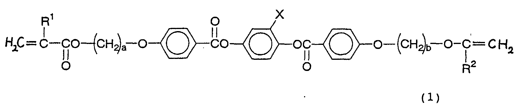
- a liquid crystal containing a compound represented by the following chemical formula (1): and a compound represented by the following chemical formula (2): in a weight ratio between 99:1 and 50:50 can be used as the nematic liquid crystal.
- R 1 , R 2 and R 3 independently represent hydrogen or methyl group
- X represents hydrogen, chlorine, bromine, iodine, an alkyl group having 1 to 4 carbon atoms, methoxy group, cyano group or nitro group
- a, b and c are an integer of 2 to 12.
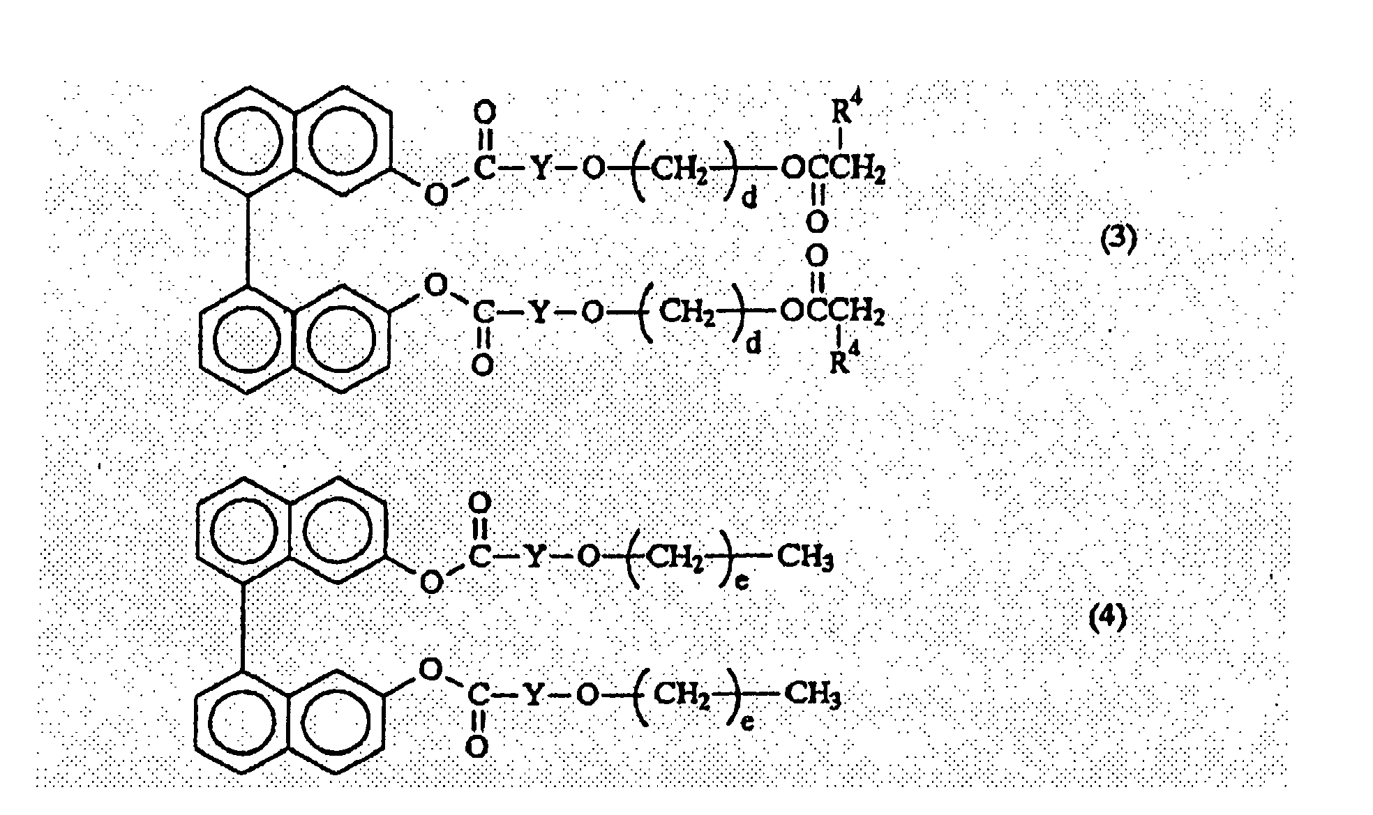
- a compound represented by the following chemical formula (3) or (4): or a chiral dopant-added liquid crystal "S-811" manufactured by Merck KGaA, Germany.
- R 4 represents hydrogen or methyl group
- d and e are an integer of 2 to 12
- Y represents a divalent group selected from the following groups (i) to (xxiv):
- a glass substrate provided with a polyimide (PI) film that has been subjected to rubbing treatment, a supporting film having the function of aligning liquid crystalline molecules, or the like is prepared as the alignment substrate 13 prepared by conducting alignment treatment.
- a liquid crystal layer is formed by the use of a radiation-curing liquid crystal having cholesteric regularity (a photo-curing chiral nematic liquid crystal, or the like). Liquid crystalline molecules in the liquid crystal layer are aligned by the alignment-regulating action of the alignment substrate 13, where the liquid crystal layer is subjected to heat treatment, if necessary.
- a predetermined amount of radiation 20 is applied to the liquid crystal layer formed on the alignment substrate 13 to three-dimensionally cross-link and cure the liquid crystal layer.
- a cholesteric layer 12 in the semi-cured state is thus formed (Fig. 2(a)).
- the radiation 20 herein used is to induce photopolymerization reaction or the like in the radiation-curing liquid crystal, and ultraviolet light, an electron beam, visible light, infrared light (heat rays), or the like can be used as the radiation.
- ultraviolet light it is preferable to add a photopolymerization initiator in the liquid crystalline material beforehand.
- the amount of the radiation 20 to be applied varies depending on whether the photopolymerization initiator has been added or not, or on the amount of the photopolymerization initiator added or the type of the radiation to be applied.
- the radiation 20 in an amount of approximately 0.01 to 10000 mJ/cm 2 , for example.
- three-dimensional crosslinking is herein meant that a photo-curing monomer, oligomer or polymer is three-dimensionally polymerized to give a network structure. If such a network structure is formed, the state of the liquid crystalline material from which the cholesteric layer 12 has been formed is optically fixed; and a film that is easy to handle as an optical film and that is stable at normal temperatures can be obtained.
- Examples of supporting films that can be used for the alignment substrate 13 include films of plastics such as polyimide, polyamideimide, polyamide, polyether imide, polyether ether ketone, polyether ketone, polyketone sulfide, polyether sulfone, polysulfone, polyphenylene sulfide, polyphenylene oxide, polyethylene terephthalate, polybutylene terephthalate, polyethylene naphthalate, polyacetal, polycarbonate, polyacrylate, acrylic resins, polyvinyl alcohol, polypropylene, cellulose, triacetyl cellulose, partially saponified triacetyl cellulose, epoxy resins, and phenol resins.
- plastics such as polyimide, polyamideimide, polyamide, polyether imide, polyether ether ketone, polyketone sulfide, polyether sulfone, polysulfone, polyphenylene sulfide, polyphenylene oxide, polyethylene terephthalate,
- plastic films may be used as a laminate of two or more films and also as uniaxially or biaxially oriented ones.
- the supporting film may be treated in advance to make its surface hydrophilic or hydrophobic.
- it may not be necessary to separately impart the function of aligning liquid crystalline molecules to the supporting film depending on the composition of the liquid crystal contained in the liquid crystalline material it is preferable to impart this function to the supporting film before applying the liquid crystalline material to the supporting film.
- an alignment layer is laminated to the supporting film, or the supporting film or the alignment layer laminated to the supporting film is rubbed. It is also possible to impart this function to the supporting film by obliquely depositing silicon oxide on the supporting film.
- Rubbing treatment is usually carried out in the following manner: a rubbing cloth made from rayon, cotton, polyamide, or the like is wrapped around a metallic roll, and this roll is rotated with its surface in contact with a film of polyimide or the like, or a film of polyimide or the like is conveyed with the roll fixed, thereby rubbing the film surface with the rubbing cloth.
- the cholesteric layer 12 in the semi-cured state, formed on the alignment substrate 13, is brought into contact with an organic solvent 21 (Fig. 2 (b)).
- an organic solvent 21 Fig. 2 (b)
- a variety of development methods such as immersion and spin shower, as well as various of coating methods such as spin coating, die coating and cast coating may be adopted.
- uncured portions of the semi-cured cholesteric layer 12 are extracted; extracted herein are uncured portions of both the nematic liquid crystal and chiral agent, which are the chief components of the cholesteric layer 12.
- a smaller amount of ultraviolet light is applied to the cholesteric layer 12, a larger part of the cholesteric layer 12 remains uncured, and vice versa.
- the semi-cured cholesteric layer 12 formed by the application of a small amount of radiation 20 is brought into contact with an organic solvent, uncured portions of the cholesteric layer 12 are extracted in a large amount, and the cholesteric layer 12 is entirely thinned. As a result, the chiral pitch becomes short, and the selective reflection wave range is shifted to the shorter wavelength side.
- the degree of shift in wavelength thus varies depending upon the state of curing (proportion of uncured portions) of the cholesteric layer 12, regardless of the conditions under which the cholesteric layer 12 is brought into contact with an organic solvent, and the selective reflection wave range of the cholesteric layer 12 is controlled by the degree of this shift (see Fig. 3).
- organic solvent 21 can be used as the organic solvent 21 in the above process as long as it can dissolve the cholesteric layer 12.
- organic solvents include: hydrocarbons such as benzene, toluene, xylene, n-butyl benzene, diethyl benzene and tetralin; ethers such as methoxybenzene, 1,2-dimethoxybenzene and diethylene glycol dimethyl ether; ketones such as acetone, methyl ethyl ketone, methyl isobutyl ketone, cyclohexanone and 2,4-pentanedione; esters such as ethyl acetate, ethylene glycol monomethyl ether acetate, propylene glycol monomethyl ether acetate, propylene glycol monoethyl ether acetate and ⁇ -butyrolactone; amide-type solvents such as 2-pyrrolidone, N-methyl-2-pyrrolidone, dimethyl
- solvents can be used either singly or in combination. Such inconveniences that the liquid crystal cannot fully be dissolved in one solvent and that one solvent is likely to dissolve the supporting film, which will be described later, can be avoided by the use of a mixture of two or more solvents.
- hydrocarbons and glycol monoether acetates are preferred as solvents to be used singly; and mixtures of ethers or ketones and glycols are preferred as solvent mixtures.
- An optical element 10 containing the cholesteric layer 12 formed on the alignment substrate 13 is thus finally obtained (Fig. 2(c)). It is preferable to subject the cholesteric layer 12 to drying and re-alignment treatment at a predetermined temperature, thereby stabilizing the optical properties of the cholesteric layer 12. It is also preferable that, after the drying and re-alignment treatment is completed, a predetermined amount of radiation (ultraviolet light or the like) be applied to the cholesteric layer 12 in the air, more preferably in an inert atmosphere, to re-cure the cholesteric layer 12.
- a predetermined amount of radiation ultraviolet light or the like
- the crystalline material for forming the cholesteric layer 12 may be made into a coating liquid by dissolving it in a solvent.
- a solvent the above-mentioned material for the organic solvent 21 can be used.
- the concentration of the solution cannot be specified sweepingly because it depends on the solubility of the liquid crystal in the solvent and the desired thickness of the liquid crystal layer to be formed. In general, however, the concentration is adjusted so that it will fall in the range of 1 to 60% by weight, preferably in the range of 3 to 40% by weight. Surface active agents, etc.
- surface active agents may be added to the liquid crystal solution in order to make it easy to apply the solution.
- surface active agents include: cationic surface active agents such as imidazoline, quaternary ammonium salts, alkylamine oxides and polyamine derivatives; anionic surface active agents such as polyoxyethylene-polyoxypropylene condensation products, primary or secondary alcohol ethoxylates, alkylphenol ethoxylates, polyethylene glycol and its esters, sodium lauryl sulfate, ammonium lauryl sulfate, amine lauryl sulfate, alkyl-substituted aromatic sulfonates, alkyl phosphates, and aliphatic or aromatic sulfonic acid-formalin condensation products; amphoteric surface active agents such as laurylamidopropylbetaine and laurylaminoacetic acid betaine; nonionic surface active agents such as polyethylene glycol fatty esters and polyoxyethylene alkyl
- the amount of a surface active agent to be added varies depending upon the type of the surface active agent, the type of the curing liquid crystal, the type of the solvent, and the type of the glass substrate or supporting film to which the liquid crystal solution is applied; and, in general, it is from 10 wt. ppm to 10% by weight, preferably from 100 wt. ppm to 5% by weight, more preferably from 0.1 to 1% by weight of the liquid crystal contained in the solution.
- the selective reflection wave range of the cholesteric layer 12 can be controlled by changing the amount of the radiation 20 to be applied to the liquid crystal layer formed on the alignment substrate 13, so that it is possible to control the selective reflection wave range of the cholesteric layer 12 with ease and high precision. It is therefore possible to easily produce an optical element 10 that comprises a cholesteric layer 12 having the desired selective reflection wave range and that is excellent in both optical stability and intensity of color.
- the radiation 20 is evenly applied to the entire surface of the liquid crystal layer formed on the alignment substrate 13.
- the present invention is not limited to this; and the radiation 20 may be applied in different amounts to different regions on the surface of the liquid crystal layer as shown in Figs. 4(a), 4(b) and 4(c) so that these regions can have different selective reflection wave ranges.
- a color filter or the like having a cholesteric layer 12 on which each pixel has selective reflection wave ranges equal to the wave ranges of red (R), green (G) and blue (B) colors.
- the cholesteric layer 12 is formed by bringing, under the specific conditions, the uniformly deposited liquid crystal layer into contact with an organic solvent, and the final thickness of the cholesteric layer 12 differs as shown in Fig. 4(c) according to the regions to which the radiation has been applied in different amounts.
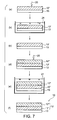
- the second embodiment of the present invention is basically the same as the first embodiment shown in Figs. 1 to 4, except that the cholesteric layer 12 is composed of a laminate of a plurality of cholesteric films 12' and 12". It is noted that like reference characters designate like or corresponding parts throughout several views and that those parts that have been explained in connection with the first embodiment will not be explained any more in detail in the description of the second embodiment.
- an optical element 10 is composed of: an alignment substrate 13 prepared by conducting alignment treatment; and a cholesteric layer 12 laminated to the alignment substrate 13.
- the cholesteric layer 12 is composed of a laminate of a plurality of cholesteric films 12' and 12" having different chiral pitches, and has a broad selective reflection wave range covering the selective reflection wave range of the cholesteric film 12' and that of the cholesteric film 12" (see Fig. 6).
- a glass substrate provided with a polyimide (PI) film that has been subjected to rubbing treatment, a supporting film having the function of aligning liquid crystalline molecules, or the like is prepared as the alignment substrate 13 prepared by conducting alignment treatment.
- a first liquid crystal layer is formed by the use of a photo-curing chiral nematic liquid crystal having cholesteric regularity. Liquid crystalline molecules in the first liquid crystal layer are aligned by the alignment-regulating action of the alignment substrate 13, where the first liquid crystal layer is subjected to heat treatment, if necessary.
- a predetermined amount (e.g., from 0.01 to 10000 mJ/cm 2 ) of radiation 20 is applied to the first liquid crystal layer formed on the alignment substrate 13 to three-dimensionally cross-link and cure the first liquid crystal layer.
- a first cholesteric film 12' is thus formed in the semi-cured state (Fig. 7(a)).
- an optical element containing the first cholesteric film 12' formed on the alignment substrate 13 (Fig. 7(c)). It is preferable to subject the first cholesteric film 12' to drying and re-alignment treatment at a predetermined temperature, thereby stabilizing the optical properties of the first cholesteric film 12'. It is also preferable that, after the drying and re-alignment treatment is completed, a predetermined amount of radiation (ultraviolet light or the like) be applied to the first cholesteric film 12' in the air, more preferably in an inert atmosphere, to re-cure the first cholesteric film 12'. Any organic solvent can be used as the organic solvent in the above process as long as it can dissolve the first cholesteric film 12'; and one of the organic solvents enumerated in the above description of the first embodiment, for example, can be used.
- a second liquid crystal layer is formed on the first cholesteric film 12' provided on the alignment substrate 13. Liquid crystalline molecules in the second crystal layer are aligned by the alignment-regulating action of the first cholesteric film 12', where the second crystal layer is subjected to heat treatment, if necessary.
- a polyimide (PI) film may be formed on the first cholesteric film 12' and rubbed. A predetermined amount of radiation 20 is applied to the second liquid crystal layer formed on the first cholesteric film 12' to three-dimensionally cross-link and cure the second liquid crystal layer. A second cholesteric film 12" is thus formed in the semi-cured state (Fig. 7 (d)).
- the semi-cured second cholesteric film 12" formed on the first cholesteric film 12' is then brought into contact with an organic solvent 21 (Fig. 7(e)).
- an optical element 10 containing the cholesteric films 12' and 12" on the alignment substrate 13 (Fig. 7 (f)). It is preferable to subject the second cholesteric film 12" to drying and re-alignment treatment at a predetermined temperature, thereby stabilizing the optical properties of the second cholesteric film 12". It is also preferable that, after the drying and re-alignment treatment is completed, a predetermined amount of radiation (ultraviolet light or the like) be applied to the second cholesteric film 12" in the air, more preferably in an inert atmosphere, to re-cure the second cholesteric film 12". Any organic solvent can be used as the organic solvent in the above process as long as it can dissolve the second cholesteric film 12"; and one of the organic solvents enumerated in the description of the first embodiment, for example, can be used.
- the liquid crystalline materials for forming the cholesteric films 12' and 12" may be made into coating liquids by dissolving them in solvents, as mentioned in the above description of the first embodiment. In this case, it is necessary to add the drying step of evaporating the solvent before three-dimensionally crosslinking each liquid crystal layer by the application of radiation 20.
- the selective reflection wave ranges of the plurality of cholesteric films 12' and 12" can be controlled by changing the amount of the radiation 20 to be applied to the liquid crystal layer formed on the alignment substrate 13 or on the first cholesteric film 12', so that it is possible to control the selective reflection wave ranges of the plurality of cholesteric films 12' and 12" with ease and high precision. It is therefore possible to easily produce an optical element 10 that comprises a cholesteric layer 12 composed of a laminate of a plurality of cholesteric films 12' and 12" having different selective reflection wave ranges and that is excellent in both optical stability and intensity of color.
- Example 1 The aforementioned first embodiment of the invention will now be explained more specifically by referring to Example 1.
- a photo-curing chiral nematic liquid crystal consisting of 80 parts by weight of a polymerizable nematic liquid crystals, 20 parts by weight of a chiral agent and 1 part by weight of a photopolymerization initiator was dissolved in toluene to obtain a 25 wt.% toluene solution of the chiral nematic liquid crystal.
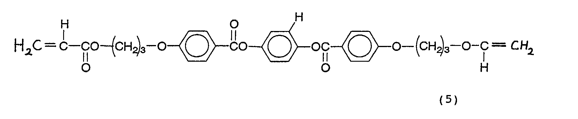
- the nematic liquid crystal used was a liquid crystal containing a compound represented by the following chemical formula (5): and a compound represented by the following chemical formula (6): in the weight ratio of 90:10. Further, a chiral dopant-added liquid crystal "S-811" (manufactured by Merck KGaA, Germany) was used as the chiral agent; and "Irg 631" (available from Ciba Specialty Chemicals K.K., Japan) was used as the photopolymerization initiator.
- S-811 manufactured by Merck KGaA, Germany
- Irg 631 available from Ciba Specialty Chemicals K.K., Japan
- a glass substrate was coated with polyimide (PI); and the polyimide film formed was rubbed in the definite direction (alignment treatment) to obtain an alignment substrate.
- PI polyimide
- the glass substrate having thereon the polyimide (PI) film that had been subjected to the rubbing treatment was set in a spin coater; and the polyimide film was spin-coated with the above-prepared toluene solution so that the thickness of the solution layer would be from about 3.0 to 5.0 ⁇ m.
- the alignment substrate coated with the toluene solution was then subjected to drying and alignment treatment with heating at 80°C for 5 minutes. It was visually confirmed that the liquid crystal layer formed on the alignment substrate was cholesteric.
- an ultraviolet light irradiator having an extra-high pressure mercury vapor lamp By the use of an ultraviolet light irradiator having an extra-high pressure mercury vapor lamp, a predetermined amount of ultraviolet light was applied to the liquid crystal layer to three-dimensionally cross-link and polymerize the liquid crystal layer. A cholesteric layer in the semi-cured state was thus formed on the alignment substrate.
- the semi-cured cholesteric layer formed on the alignment substrate was immersed in acetone for 5 minutes.
- this cholesteric layer was dried with heating at 60°C for 15 minutes; and 10000 mJ/cm 2 of ultraviolet light was applied to the cholesteric layer by an ultraviolet light irradiator having an extra-high pressure mercury vapor lamp to re-cure the cholesteric layer, thereby stabilizing the optical properties of the cholesteric layer.
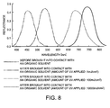
- ultraviolet light was applied in three different amounts, 1 mJ/cm 2 , 100 mJ/cm 2 and 10000 mJ/cm 2 , to form three cholesteric layers in the semi-cured state, and the selective reflection wavelengths (reflection spectra) of the finally-obtained three optical elements were measured by a spectrophotometer.
- the results are shown in Fig. 8. Shift to the shorter wavelength side was confirmed in the selective reflection wave range of each cholesteric layer after the cholesteric layer was brought into contact with the organic solvent; and the degree of this shift was found to be greater when the amount of ultraviolet light applied was smaller.
- the bandwidth of the selective reflection wave range was approximately 80 nm in all cases.
- Example 2 an optical element was produced in the same manner as that of Example 1 except that 3 parts by weight of "Irg 369” (available from Ciba Specialty Chemicals K.K., Japan) was used as the photopolymerization initiator, instead of 1 part by weight of "Irg 631.”
- Irg 369 available from Ciba Specialty Chemicals K.K., Japan
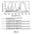
- Example 2 ultraviolet light was applied in four different amounts, 4 mJ/cm 2 , 8 mJ/cm 2 , 20 mJ/cm 2 and 400 mJ/cm 2 , to form four cholesteric layers in the semi-cured state, and the selective reflection wavelengths (reflection spectra) of the finally-obtained four optical elements were measured by a spectrophotometer. The results are shown in Fig. 9. Similar to Example 1, shift to the shorter wavelength side was confirmed in the selective reflection wave range of each cholesteric layer after the cholesteric layer was brought into contact with the organic solvent. This shift was accomplished with a smaller amount of ultraviolet light as compared with Example 1.
- a photo-curing chiral nematic liquid crystal consisting of 80 parts by weight of a polymerizable nematic liquid crystal, 20 parts by weight of a chiral agent and 1 part by weight of a photopolymerization initiator was dissolved in toluene to obtain a 25 wt.% toluene solution of the chiral nematic liquid crystal.
- the nematic liquid crystal, the chiral agent and the photopolymerization initiator used in this example were the same as those used in Example 1.
- a glass substrate was coated with polyimide (PI); and the polyimide film formed was rubbed in the definite direction (alignment treatment) to obtain an alignment substrate.
- PI polyimide
- the glass substrate having thereon the polyimide (PI) film that had been subjected to the rubbing treatment was set in a spin coater, and the polyimide film was spin-coated with the above-prepared toluene solution so that the thickness of the solution layer would be from about 3.0 to 5.0 ⁇ m.
- the alignment substrate coated with the toluene solution was then subjected to drying and alignment treatment with heating at 80°C for 5 minutes. It was visually confirmed that the layer formed on the alignment substrate was cholesteric.
- an ultraviolet light irradiator having an extra-high pressure mercury vapor lamp By the use of an ultraviolet light irradiator having an extra-high pressure mercury vapor lamp, a predetermined amount of ultraviolet light was applied to the liquid crystal layer to three-dimensionally cross-link and polymerize the liquid crystal layer. A first cholesteric film in the semi-cured state was thus formed on the alignment substrate.
- the semi-cured first cholesteric film formed on the alignment substrate was immersed in acetone for 5 minutes.
- the first cholesteric film that had been immersed in acetone was spin-coated with the above-prepared toluene solution so that the thickness of the solution layer would be from about 3.0 to 5.0 ⁇ m.
- This layer was then subjected to drying and alignment treatment with heating at 80°C for 5 minutes. It was visually observed that the layer formed on the first cholesteric film was cholesteric.
- the semi-cured second cholesteric film formed on the first cholesteric film was then immersed in acetone for 5 minutes.
- This cholesteric film was dried with heating at 60°C for 15 minutes. 10000 mJ/cm 2 of ultraviolet light was then applied to the cholesteric layer by an ultraviolet light irradiator having an extra-high pressure mercury vapor lamp to re-cure the cholesteric layer, thereby stabilizing the optical properties of the cholesteric layer.
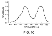
- the optical element containing the cholesteric layer composed of the laminate of the two cholesteric films, formed by applying ultraviolet light in different amounts was found to have the optical properties (broad selective reflection wave range) covering the optical properties (selective reflection wave range) of the first cholesteric film and those of the second cholesteric film, as shown in Fig. 10.
Landscapes
- Physics & Mathematics (AREA)
- Chemical & Material Sciences (AREA)
- Crystallography & Structural Chemistry (AREA)
- General Physics & Mathematics (AREA)
- Optics & Photonics (AREA)
- Polarising Elements (AREA)
- Liquid Crystal (AREA)
- Optical Filters (AREA)
- Photosensitive Polymer And Photoresist Processing (AREA)
- Materials For Photolithography (AREA)
Abstract
Description



Claims (9)
- A process of producing an optical element, comprising:wherein the amount of radiation to be applied to the liquid crystal layer in the second step is changed to control a selective reflection wave range of the cholesteric layer.the first step of forming a radiation-curing liquid crystal layer having cholesteric regularity on an alignment substrate having an aligning function;the second step of applying a predetermined amount of radiation to the liquid crystal layer formed on the alignment substrate to cure the liquid crystal layer, thereby forming a cholesteric layer in the semi-cured state; andthe third step of bringing the semi-cured cholesteric layer formed on the alignment substrate into contact with an organic solvent;
- The process according to claim 1, wherein the radiation is applied, in the second step, in different amounts to different regions on the surface of the liquid crystal layer so that these regions can have different selective reflection wave ranges.
- The process according to claim 1 or 2, wherein the radiation to be applied to the liquid crystal layer in the second step is light selected from the group consisting of ultraviolet light, an electron beam, visible light and infrared light.
- The process according to claim 1, 2 or 3, wherein the liquid crystal layer formed in the first step comprises a chiral nematic liquid crystal obtained by adding a chiral agent to a nematic liquid crystal.
- A process of producing an optical element, comprising:wherein the amount of radiation to be applied to the first or second liquid crystal layer in the second or fifth step is changed to control a selective reflection wave range of the first or second cholesteric film.the first step of forming a first radiation-curing liquid crystal layer having cholesteric regularity on an alignment substrate having an aligning function;the second step of applying a predetermined amount of radiation to the first liquid crystal layer formed on the alignment substrate to cure the first liquid crystal layer, thereby forming a first cholesteric film in the semi-cured state;the third step of bringing the semi-cured first cholesteric film formed on the alignment substrate into contact with an organic solvent;the fourth step of forming a second radiation-curing liquid crystal layer having cholesteric regularity on the first cholesteric film that has been brought into contact with the organic solvent;the fifth step of applying a predetermined amount of radiation to the second liquid crystal layer formed on the first cholesteric film to cure the second liquid crystal layer, thereby forming a second cholesteric film in the semi-cured state; andthe sixth step of bringing the semi-cured second cholesteric film formed on the first cholesteric film into contact with an organic solvent;
- The process according to claim 5, wherein the radiation to be applied to the first and second liquid crystal layer in the second and fifth steps is light selected from the group consisting of ultraviolet light, an electron beam, visible light and infrared light.
- The process according to claim 5 or 6, wherein the first and second liquid crystal layers formed in the first and fourth steps comprise a chiral nematic liquid crystal obtained by adding a chiral agent to a nematic liquid crystal.
- An optical element comprising a cholesteric layer having cholesteric regularity, wherein the cholesteric layer has a plurality of regions that are made different in thickness so that they can have different selective reflection wave ranges.
- The optical element according to claim 8, wherein the regions in the cholesteric layer have selective reflection wave ranges equal to wave ranges of red, green and blue colors to compose a pixel.
Applications Claiming Priority (2)
| Application Number | Priority Date | Filing Date | Title |
|---|---|---|---|
| JP2001324808 | 2001-10-23 | ||
| JP2001324808A JP2003131031A (en) | 2001-10-23 | 2001-10-23 | Method for manufacturing optical element and optical element |
Publications (3)
| Publication Number | Publication Date |
|---|---|
| EP1306699A2 true EP1306699A2 (en) | 2003-05-02 |
| EP1306699A3 EP1306699A3 (en) | 2003-07-23 |
| EP1306699B1 EP1306699B1 (en) | 2006-12-13 |
Family
ID=19141480
Family Applications (1)
| Application Number | Title | Priority Date | Filing Date |
|---|---|---|---|
| EP02023556A Expired - Lifetime EP1306699B1 (en) | 2001-10-23 | 2002-10-22 | Process of producing optical element and optical element |
Country Status (4)
| Country | Link |
|---|---|
| US (2) | US7118795B2 (en) |
| EP (1) | EP1306699B1 (en) |
| JP (1) | JP2003131031A (en) |
| DE (1) | DE60216703T2 (en) |
Cited By (2)
| Publication number | Priority date | Publication date | Assignee | Title |
|---|---|---|---|---|
| WO2007057807A3 (en) * | 2005-11-17 | 2007-11-01 | Koninkl Philips Electronics Nv | Vcsel with coating for polarization control |
| CN100485481C (en) * | 2004-06-04 | 2009-05-06 | 长兴化学工业股份有限公司 | Optical film and method for producing same |
Families Citing this family (11)
| Publication number | Priority date | Publication date | Assignee | Title |
|---|---|---|---|---|
| JP2005084331A (en) * | 2003-09-08 | 2005-03-31 | Fuji Photo Film Co Ltd | Display device, image display apparatus, and display method |
| JP2007519941A (en) * | 2003-11-21 | 2007-07-19 | メルク パテント ゲゼルシャフト ミット ベシュレンクテル ハフトング | Method for modifying chiral liquid crystal membrane using extractant |
| TW200628938A (en) * | 2005-02-02 | 2006-08-16 | Quanta Display Inc | Substrate of a liquid crystal display and method of forming an alignment layer |
| JP4612451B2 (en) * | 2005-03-30 | 2011-01-12 | 大日本印刷株式会社 | Photosensitive composition, optical element using the same, and method for producing the same |
| JP4670453B2 (en) * | 2005-04-19 | 2011-04-13 | セイコーエプソン株式会社 | Inorganic oxide film processing method, liquid crystal panel manufacturing method |
| JP5540473B2 (en) * | 2008-06-12 | 2014-07-02 | 凸版印刷株式会社 | Cholesteric liquid crystal display supplies |
| KR20100003565A (en) * | 2008-07-01 | 2010-01-11 | 삼성전자주식회사 | Method of manufacturing liquid crystal display |
| WO2010143682A1 (en) * | 2009-06-11 | 2010-12-16 | 富士フイルム株式会社 | Process for production of light reflection film |
| JP2011137855A (en) * | 2009-12-25 | 2011-07-14 | Dainippon Printing Co Ltd | Method for manufacturing electromagnetic wave reflection member |
| JP6765429B2 (en) * | 2016-08-30 | 2020-10-07 | 富士フイルム株式会社 | Optical laminate |
| JP6878662B1 (en) * | 2020-08-28 | 2021-06-02 | 日東電工株式会社 | Manufacturing method of oriented liquid crystal film |
Family Cites Families (24)
| Publication number | Priority date | Publication date | Assignee | Title |
|---|---|---|---|---|
| DE2805970C3 (en) * | 1978-02-13 | 1980-09-25 | Siemens Ag, 1000 Berlin Und 8000 Muenchen | Liquid crystal display device |
| US5235443A (en) | 1989-07-10 | 1993-08-10 | Hoffmann-La Roche Inc. | Polarizer device |
| US5267060A (en) | 1990-09-28 | 1993-11-30 | Rockwell International Corporation | Reflective color light filter and method of manufacture |
| JPH07112155B2 (en) | 1990-11-16 | 1995-11-29 | 株式会社東芝 | Switching constant current source circuit |
| US5221982A (en) | 1991-07-05 | 1993-06-22 | Faris Sadeg M | Polarizing wavelength separator |
| GB9121159D0 (en) | 1991-10-04 | 1991-11-13 | Marconi Gec Ltd | Colour display system |
| US5691789A (en) * | 1995-10-30 | 1997-11-25 | Li; Le | Single-layer reflective super broadband circular polarizer and method of fabrication therefor |
| TW289095B (en) | 1993-01-11 | 1996-10-21 | ||
| US5486935A (en) | 1993-06-29 | 1996-01-23 | Kaiser Aerospace And Electronics Corporation | High efficiency chiral nematic liquid crystal rear polarizer for liquid crystal displays having a notch polarization bandwidth of 100 nm to 250 nm |
| US5644415A (en) * | 1993-12-20 | 1997-07-01 | Casio Computer Co., Ltd. | Liquid crystal display device having wide field angle |
| JPH0954212A (en) | 1995-08-11 | 1997-02-25 | Sharp Corp | Retardation film, manufacturing method thereof, and liquid crystal display device |
| JPH1054905A (en) | 1996-08-12 | 1998-02-24 | Nitto Denko Corp | Multicolor reflector |
| GB2321717A (en) | 1997-01-31 | 1998-08-05 | Sharp Kk | Cholesteric optical filters |
| DE19718293A1 (en) | 1997-04-30 | 1999-03-18 | Consortium Elektrochem Ind | Process for the production of three-dimensionally cross-linked polymeric materials with broad cholesteric reflection bands and filters, reflectors and polarizers produced by this process |
| KR100655770B1 (en) | 1998-12-07 | 2006-12-12 | 코닌클리케 필립스 일렉트로닉스 엔.브이. | Polymer material pattern layer having cholesteric arrangement and method for producing same |
| EP1045272A3 (en) * | 1999-04-12 | 2004-02-25 | Matsushita Electric Industrial Co., Ltd. | Reflective color liquid crystal display device |
| JP2000345160A (en) | 1999-06-04 | 2000-12-12 | Nippon Mitsubishi Oil Corp | Liquid crystal composition and liquid crystal film using the composition |
| KR100675997B1 (en) | 1999-07-02 | 2007-01-29 | 메르크 파텐트 게엠베하 | Manufacturing method of multilayer cholesteric film |
| KR100675996B1 (en) * | 1999-07-02 | 2007-01-29 | 메르크 파텐트 게엠베하 | Manufacturing method of multilayer cholesteric film |
| JP2001159706A (en) | 1999-12-02 | 2001-06-12 | Fuji Photo Film Co Ltd | Method of manufacturing cholesteric liquid crystal color filter |
| US6714276B2 (en) * | 2000-02-08 | 2004-03-30 | Sharp Kabushiki Kaisha | Liquid crystal display device |
| JP2001242315A (en) | 2000-02-29 | 2001-09-07 | Fuji Photo Film Co Ltd | Cholesteric liquid crystal color filter, method of manufacturing the same, and display device using the same |
| JP3683172B2 (en) * | 2000-11-09 | 2005-08-17 | シャープ株式会社 | Liquid crystal display element |
| TW565712B (en) * | 2001-10-16 | 2003-12-11 | Dainippon Printing Co Ltd | Method of producing optical element by patterning liquid crystal films |
-
2001
- 2001-10-23 JP JP2001324808A patent/JP2003131031A/en not_active Withdrawn
-
2002
- 2002-10-21 US US10/274,373 patent/US7118795B2/en not_active Expired - Fee Related
- 2002-10-22 EP EP02023556A patent/EP1306699B1/en not_active Expired - Lifetime
- 2002-10-22 DE DE60216703T patent/DE60216703T2/en not_active Expired - Fee Related
-
2006
- 2006-08-30 US US11/512,166 patent/US20060292296A1/en not_active Abandoned
Cited By (2)
| Publication number | Priority date | Publication date | Assignee | Title |
|---|---|---|---|---|
| CN100485481C (en) * | 2004-06-04 | 2009-05-06 | 长兴化学工业股份有限公司 | Optical film and method for producing same |
| WO2007057807A3 (en) * | 2005-11-17 | 2007-11-01 | Koninkl Philips Electronics Nv | Vcsel with coating for polarization control |
Also Published As
| Publication number | Publication date |
|---|---|
| DE60216703D1 (en) | 2007-01-25 |
| US20060292296A1 (en) | 2006-12-28 |
| DE60216703T2 (en) | 2007-10-04 |
| EP1306699B1 (en) | 2006-12-13 |
| EP1306699A3 (en) | 2003-07-23 |
| US20030077421A1 (en) | 2003-04-24 |
| US7118795B2 (en) | 2006-10-10 |
| JP2003131031A (en) | 2003-05-08 |
Similar Documents
| Publication | Publication Date | Title |
|---|---|---|
| US7495731B2 (en) | Retardation element, display element comprising the same, and process of producing retardation element | |
| TWI547735B (en) | Liquid crystal device | |
| TWI645974B (en) | Laminated body | |
| US7897304B2 (en) | Color filter, semi-transmissive semi-reflective liquid-crystal display device, method for forming phase difference control layer, and method for manufacturing color filter | |
| CN1997920B (en) | Method for manufacturing multilayer cholesteric liquid crystal optical bodies | |
| EP1306699B1 (en) | Process of producing optical element and optical element | |
| US20060103796A1 (en) | Elliptically polarizing plate and image display apparatus using the same | |
| KR20200110182A (en) | Image display apparatus and circularly polarizing plate to be used in the image display apparatus | |
| JP2006178389A (en) | Manufacturing method of elliptically polarizing plate and image display device using elliptically polarizing plate | |
| JP2007298967A (en) | Film, film manufacturing method, and use thereof | |
| US20060033861A1 (en) | Optical device | |
| EP1445628A1 (en) | METHOD FOR MAKING CIRCULARLY−POLARIZED LIGHT CONTROL OPTICAL DEVICE | |
| JP7440523B2 (en) | Liquid crystal composition, optical film, circularly polarizing plate for organic EL display, manufacturing method of optically anisotropic layer | |
| JP5209223B2 (en) | Film, film manufacturing method, and use thereof | |
| CN116113858B (en) | Method for manufacturing optical anisotropic layers | |
| JP2008209652A (en) | Manufacturing method of elliptically polarizing plate | |
| CN109416429B (en) | Vertical alignment liquid crystal film and its manufacturing method | |
| KR100728427B1 (en) | Method for manufacturing optical device, optical device, optical film using optical device, lighting device and liquid crystal display device using optical device or optical film | |
| JP2006201746A (en) | Elliptical polarizing plate and image display device using the same | |
| WO2006090520A1 (en) | Process for producing elliptical polarization plate and image display apparatus utilizing elliptical polarization plate | |
| Parri et al. | Patterned retarder films using reactive mesogen technology | |
| JP4592046B2 (en) | Manufacturing method of optical film | |
| JP3728212B2 (en) | Circularly polarized light extracting optical element, polarized light source device, and liquid crystal display device | |
| CN118575107A (en) | Antireflection film and organic electroluminescent display device | |
| JP4251473B2 (en) | Method for producing cholesteric liquid crystal color filter |
Legal Events
| Date | Code | Title | Description |
|---|---|---|---|
| PUAI | Public reference made under article 153(3) epc to a published international application that has entered the european phase |
Free format text: ORIGINAL CODE: 0009012 |
|
| AK | Designated contracting states |
Designated state(s): AT BE BG CH CY CZ DE DK EE ES FI FR GB GR IE IT LI LU MC NL PT SE SK TR |
|
| AX | Request for extension of the european patent |
Extension state: AL LT LV MK RO SI |
|
| PUAL | Search report despatched |
Free format text: ORIGINAL CODE: 0009013 |
|
| AK | Designated contracting states |
Designated state(s): AT BE BG CH CY CZ DE DK EE ES FI FR GB GR IE IT LI LU MC NL PT SE SK TR |
|
| AX | Request for extension of the european patent |
Extension state: AL LT LV MK RO SI |
|
| 17P | Request for examination filed |
Effective date: 20031016 |
|
| AKX | Designation fees paid |
Designated state(s): DE GB NL |
|
| GRAP | Despatch of communication of intention to grant a patent |
Free format text: ORIGINAL CODE: EPIDOSNIGR1 |
|
| GRAS | Grant fee paid |
Free format text: ORIGINAL CODE: EPIDOSNIGR3 |
|
| GRAA | (expected) grant |
Free format text: ORIGINAL CODE: 0009210 |
|
| AK | Designated contracting states |
Kind code of ref document: B1 Designated state(s): DE GB NL |
|
| REG | Reference to a national code |
Ref country code: GB Ref legal event code: FG4D |
|
| REF | Corresponds to: |
Ref document number: 60216703 Country of ref document: DE Date of ref document: 20070125 Kind code of ref document: P |
|
| PLBE | No opposition filed within time limit |
Free format text: ORIGINAL CODE: 0009261 |
|
| STAA | Information on the status of an ep patent application or granted ep patent |
Free format text: STATUS: NO OPPOSITION FILED WITHIN TIME LIMIT |
|
| 26N | No opposition filed |
Effective date: 20070914 |
|
| GBPC | Gb: european patent ceased through non-payment of renewal fee |
Effective date: 20071022 |
|
| NLV4 | Nl: lapsed or anulled due to non-payment of the annual fee |
Effective date: 20080501 |
|
| PG25 | Lapsed in a contracting state [announced via postgrant information from national office to epo] |
Ref country code: DE Free format text: LAPSE BECAUSE OF NON-PAYMENT OF DUE FEES Effective date: 20080501 |
|
| PG25 | Lapsed in a contracting state [announced via postgrant information from national office to epo] |
Ref country code: NL Free format text: LAPSE BECAUSE OF NON-PAYMENT OF DUE FEES Effective date: 20080501 |
|
| PG25 | Lapsed in a contracting state [announced via postgrant information from national office to epo] |
Ref country code: GB Free format text: LAPSE BECAUSE OF NON-PAYMENT OF DUE FEES Effective date: 20071022 |