TECHNICAL FIELD
The present invention relates to an optical fiber transmission system
and an optical transmitter used in the system.
BACKGROUND ART
(SPM-GVD Degradation)
The intensity modulation- direct detection method is widely adopted
in existing fiber optic telecommunication systems. According to the
method, digital information is placed on intensity of signal light and the
intensity is directly detected by an optical power detector. Besides, the
capacity of the systems is enlarged by wavelength-division multiplexing.
In the transmission systems, chromatic dispersion (GVD: Group Velocity
Dispersion) in an optical fiber and self-phase modulation (SPM) effect in
combination induces a phenomenon called SPM-GVD effect. SPM is one
of the nonlinear optical effects arise in the optical fiber. A waveform
distortion resulting from the SPM-GVD effect is a main factor in
transmission degradation. Higher power of the signal light in the optical
fiber encourages the degradation due to the nonlinear optical effects such as
the SPM-GVD effect.
(Optical SNR Degradation and Trade-Off in the Output Power of
Repeaters)
Another main factor in transmission degradation is accumulation of
optical noises called optical SNR (Signal to Noise Ratio) degradation
attendant on optical amplifying relay. This deteriorating effect is
increased as input power to an optical amplifying repeater becomes lower.
Thus, provided that section losses between respective repeaters are constant,
there is an optimal value for the output power of the repeaters. Expressing
the performance of a transmission system in terms of bit-error-rate (BER),
BER is deteriorated by the nonlinear optical effects when the repeater
output power is excessive. On the other hand, when the repeater output
power is insufficient, BER is deteriorated by the optical SNR degradation.
In this manner, there are two limiting factors showing opposite tendencies
in the output power of the repeaters. Therefore, it is a technical subject
how to loosen the trade-off relation and how to increase allowable loss in
repeater sections.
(Chirp)
In the optical communication field, phase change according to
intensity change in the carrier (light) is referred to as chirp. SPM is also a
kind of the chirp, and its direction in most mediums like the optical fiber is
expressed as Kerr coefficient n2 > 0, that is, the direction in which a
phase-delay in the carrier is increased as instantaneous intensity gets higher.
Hereinafter the direction of the chirp is indicated by whether the chirp is in
a SPM direction or in a counter- SPM direction on the basis of the phase
shift direction of SPM. Besides, advance chirp in a transmitter is referred
to as prechirp.
In the history of the development of optical transmission techniques,
the prechirp was initially studied as one of the dispersion compensation
techniques (e.g. Saito et al., "Prechirp Technique for Disperson
Compensation for a High-Speed Long-Span Transmission", Photon.
Technol. Lett., p.74, 1991). Since the high-integrity dispersion
compensating device was not well-developed in those days, the prechirp
technique was under review as one of the means to counter the waveform
distortion due to accumulations of chromatic dispersion (GVD). However,
with the emergence of excellent dispersion compensating devices such as
dispersion compensating fiber, the prechirp technique ceased to be
employed for the dispersion compensation.
(Actual Fiber Dispersion Value and SPM-GVD Effect)
The degree of SPM-GVD degradation varies according to the
chromatic dispersion value of each optical fiber line. As is known for the
mechanism of optical soliton transmission, when an SPM chirp occurs
during the transmission of light pulses in abnormal dispersion, the pulses
are compressed. As pulse form gets sharpened due to the compression,
SPM is more easily induced. On the contrary, in the case of propagation in
normal dispersion, SPM is restrained because the pulses are spread and
flattened by the SPM chirp. Therefore, transmission lines with normal
dispersion suffer less SPM-GVD degradation unless the pulse compression
effect by SPM is in positive use as in the soliton transmission.
Incidentally, in capacity enlargement techniques by the
wavelength-division multiplexing (WDM), which have been rapidly
commercialized in recent years, there is the problem of crosstalk between
channels caused by the nonlinear effect of the optical fiber. As an
effective measure to restrain the crosstalk, in general, the dispersion value
of the optical fiber is increased to make a big difference in the propagation
velocity of the respective wavelength channels.
In the vicinity of 1.55µm band that is used most in the optical
transmission system, silica (SiO2) glass fibers possess the characteristic of
abnormal material dispersion (the shorter wavelength provides the faster
propagation velocity). The dispersion value is about +17ps/ nm/ km, and
the optical fibers that maintain this material dispersion property are called
single-mode-fiber (SMF) (ITU-T Recommendations G.652). On the other
hand, optical fibers called dispersion shift fiber are also in practical use.
In the dispersion shift fiber, large normal dispersion is generated by
structural dispersion to counteract the material dispersion. The structural
dispersion, however, only negates the material dispersion at the best, and it
is technically difficult to give the fiber a large normal dispersion value.
Additionally, in the case of producing the large normal dispersion by the
structural dispersion, the cross-sectional area of the optical fiber core gets
smaller. Accordingly, there arises a problem that the nonlinear optical
effects are easily induced.
To sum up, it is preferable that line fibers are provided with the
normal dispersion value in the view of the suppression of the SPM-GVD
degradation. On the other hand, the optical fiber with a large dispersion
value required for WDM is limited to SMF being an abnormal dispersion
fiber, which makes it more important to take measures against the
SPM-GVD degradation.
(The Operation of Two-Beam Interferometer Type Optical Modulator)
In the following, a description will be given of an LN (LiNbO3)
modulator much used in the embodiments of the present invention. The
modulator has the composition of a two-beam interferometer
(Mach-Zehnder interferometer) as shown in Fig. 10. In the modulator, two
light waves, each of which has undergone a phase shift according to an
drive signal at the phase-modulating section of each arm, interfere with one
another and become output signal light.
Fig. 11(a) - (c) are diagrams showing the operation by phasor. The
distance from the origin (the center of each diagram) indicates amplitude.
On the other hand, having set the positive direction of a real axis (real) to
zero, a phase shift amount is designated by the arc of rotation from zero.
The rotation in a clockwise direction indicates a phase delay. Thin arrows
denote the lights passing through arm 1 (t) and arm 2 (t), and heavy arrows
denote a composite vector thereof as interference output light S (t). Next,
state transition will be described by following time t1, t2 to t3. At the
point of starting point t1, the vectors of arm 1 (t1) and arm 2 (t1) are in
unity, and composite vector S (t1) is at its maximum. In other words, the
power transmittance is at its maximum in the modulator as a whole.
Fig. 11(a) is a diagram for explaining the operation of
push-pull-driven chirpless modulation. Arm 1 and arm 2 are driven by a
pair of complementary electrical signals. The pair of complementary
electrical signals are two electrical signals a sum of which is invariable.
As to the actual method for generating the pair, a pair of electrical signals
each having a polarity opposite to each other can be obtained by using a
inverting amplifier or a delay line in the case of using a narrowband signal
as a clock signal.
With the push-pull drive, the lights of both the arm shift in a balanced
manner. Consequently, the composite vector traces on the real axis, and a
phase rotation (= chirp) does not occur. When each light phase-shifts from
0 to π/2 (rad) (t1 to t2), composite vector S (t2) becomes zero. Fig. 11(a)
also illustrates the state when each light further phase-shifts to π (rad).
When the lights have passed π/2, light power transmittance is increased
again and, eventually, the composite vector shifts to composite vector S (t3)
which is the same as composite vector S (t1) in intensity and opposite in
phase.
Fig. 11(b) is a diagram showing the state where only arm 1 in Fig.
11(a) is shifted from 0 to π (rad) so that the light power transmittance is
decreased from its maximum to minimum. In Fig. 11(b), a midway point
of the shift (t2) is also illustrated. In this case, the composite vector shifts
toward zero in an arc accompanied by a phase rotation according to
intensity, namely, chirp. Thus, the chirp occurs when the ratio of the
phase shift amounts of arm 1 and arm 2 does not stand at 1 to 1.
Fig. 11(c) is a diagram showing the case where the ratio of the phase
shift amounts of arm 1 and arm 2 takes the middle of those in Figs. 11(a)
and 11(b)
As can be seen in Fig. 11(a) to (c), the ratio of the phase shift amounts
of the respective arms defines the chirp. In the following, a description
will be given of how to control the ratio of the phase shift amounts in an
actual LiNbO3 (LN) modulator in reference with Fig. 12. Fig. 12(a) to (c)
shows a frame format of a Mach-Zehnder interferometer formed on a LN
substrate, being taken on line (A) of Fig. 10. In the LN substrate, Z axis is
provided with a high electro-optic coefficient as compared to X and Y axes
with respect to crystal orientation, and the LN substrate is generally
constructed so that modulating electric field is applied along Z axis.
Fig. 12(a) is a sectional view showing the configuration of a "Z
axis-cut, X (Y) axis-propagation (two-signal driven)" modulator used in a
conventional CS-RZ transmitter. As shown in Fig. 10, the modulator has a
degree of freedom to perform independent phase shifts for the two arms.
In the conventional CS-RZ transmitter, the chirpless modulation as shown
in Fig. 11(a) is implemented by inputting a pair of complementary electrical
signals to the arms.
Fig. 12(b) is a sectional view showing the configuration of a "Z
axis-cut, X (Y) axis-propagation (one-signal driven)" modulator most
widely used today. In this configuration, electric field opposite in
direction to a HOT pole is partly applied to a waveguide beneath a GND
pole. The phase shifts in the respective arms provide opposite phases
although the amplitudes are imbalanced, resulting in the modulating
operation as shown in Fig. 11(c). With this configuration, output light
undergoes the phase shift (chirp) involved in intensity modulation.
In the general usage of the LN modulator, the modulator is operated in
such a manner that its light power transmittance is decreased from the
maximum to minimum. This configuration is preferred mainly by reason
that less drive signal amplitude (referred to as V π) is required to decrease
the light power transmittance from the maximum to minimum as compared
to the configuration of Fig. 12(a) for performing the modulation as shown in
Fig. 11(b).
Fig. 12(c) is a sectional view showing the configuration of an "X (Y)
axis-cut, Y (X) axis-propagation (one-signal driven)" modulator. The "X
(Y) axis-cut, Y (X) axis-propagation" means "X axis-cut, Y
axis-propagation" or "Y axis-cut, X axis-propagation". With this
configuration, mutually complementary phase shifts can be carried out in
the two arms by only one drive signal. In other words, the chirpless
modulation can be performed as in the case of Fig. 12(a). However, it is
impossible to perform independent phase shifts in the respective arms.
(CS - RZ)
There are differences in the degree of waveform degradation by
SPM-GVD depending on modulation methods. There has been proposed
CS- RZ (Carrier-Suppressed Return-to-Zero) modulation as a modulation
method which is less apt to cause the SPM-GVD degradation by Miyamoto
et al., NTT (Y. Miyamoto et al., "320 Gbit/s (8 × 40 Gbit/s) WDM
transmission over 367-km zero-dispersion-flattened line with 120-km
repeater spacing using carrier-suppressed return-to-zero pulse format",
Optical Amplifiers and its Applications, PDP, 1999).
Fig. 13 is a diagram showing the configuration of a modulator to
which the method is applied. The modulator is separated into a data
modulating section 131 and a clock modulating section 132. Each section
is provided with a push-pull type LiNbO3 (LN) modulator that requires two
drive signals as an optical modulator. The respective LN modulators are
driven by a pair of complementary electrical signals, and output chirpless
optical modulation signals.
In the data modulating section 131, the LN modulator is driven by a
pair of complementary data signals in NRZ (Non-Return-to-Zero) code.
In the clock modulating section 132, the LN modulator is driven by a
pair of complementary clock signals. Besides, the frequency of the signals
is set to a half of bit rate frequency. For example, in the case of a bit rate
of 40Gb/s, 20GHz clock signals are used as the drive signals. Hereinafter
a clock signal of bit rate frequency is referred to as CLK, and a clock signal
whose frequency is a half of the bit rate frequency is referred to as 1/2 CLK.
Fig. 14 is a diagram showing modulating operation when a bias point,
namely, setting at the time of 0V input, of the LN modulator used in the
clock modulating section 132 is set to the point where light becomes off.
Assuming that light input is CW (Continuous Wave) light for the sake of
simplicity, the frequency of the clock pulse of modulated output light is
twice of input clock frequency in terms of power, and the phase is reversed
with respect to each 1 bit. In the view of the spectrum of the light clock
signal, a carrier is suppressed. Thus, the light clock signal is called CS
(Carrier-Suppressed) clock signal.
By connecting the NRZ data modulating section 131 and CS clock
modulating section 132 in series, logical product between the modulators
are obtained, and digital information based on the presence of pulse is
placed on a clock pulse train whose phase is reversed with respect to each 1
bit. While CS clock modulation is carried out after data modulation in Fig.
13, the same modulated light can be attained in the opposite order.
A CS-RZ modulation signal has three symbols: 1, 0 and -1. The
signal amplitude is standardized as 1. 1 and -1 indicates reversed phase
relation. When performing direct demodulation (square-law detection) of
the signal with the use of an optical power detector, 1 and -1 are equated
with each other, thus original binary signals can be obtained.
The CS-RZ modulation induces less SPM-GVD degradation as
compared to the conventional RZ modulation. Hereinafter resistance
against the SPM-GVD waveform degradation is referred to as SPM-GVD
resistance.
The configuration of a transmitter-receiver for adopting the CS-RZ
modulation is not largely different from the configuration of a
transmitter-receiver performing the ordinal RZ modulation. Therefore,
there is no rapid progress in manufacturing technique for the
transmitter-receiver, which facilitates the introduction of the method.
PROBLEMS THAT THE INVENTION IS TO SOLVE
Although the SPM-GVD resistance can be increased by the
conventional CS-RZ modulation as compared to the ordinary RZ
modulation, further improvement in the CS-RZ modulation is desired. It is
therefore an object of the present invention to provide an optical transmitter
for adopting the CS-RZ modulation to increase the SPM-GVD resistance,
and an optical fiber transmission system having the same.
DISCLOSURE OF THE INVENTION
In accordance with an aspect of the present invention, there is
provided an optical transmitter comprising: a carrier source for generating a
carrier; a data modulating section for intensity-modulating the carrier with a
data signal; and a clock modulating section for amplitude-modulating the
carrier so that the phase of the carrier is inverted for every one-bit slot of
the data signal; wherein the carrier is given a prechirp by the carrier source
or the data modulating section.
In accordance with another aspect of the present invention, in the
optical transmitter, the direction of the prechirp is opposite to that of a chirp
resulting from self-phase modulation (SPM) effect produced in an optical
fiber line.
In accordance with another aspect of the present invention, in the
optical transmitter, the waveform of the data signal is in conformity with the
NRZ modulation format.
In accordance with another aspect of the present invention, in the
optical transmitter, the waveform of the data signal is in conformity with the
RZ modulation format.
In accordance with another aspect of the present invention, in the
optical transmitter, the data modulating section includes a chirp-giving
two-beam interferometer type optical modulator.
In accordance with another aspect of the present invention, in the
optical transmitter, the chirp-giving two-beam interferometer type optical
modulator is built up on a LiNbO3 substrate.
In accordance with another aspect of the present invention, in the
optical transmitter, the chirp-giving two-beam interferometer type optical
modulator is built up on an optical semiconductor substrate.
In accordance with another aspect of the present invention, in the
optical transmitter, the data modulating section includes a chirp-giving
electroabsorption (EA) intensity modulator.
In accordance with another aspect of the present invention, in the
optical transmitter, the clock modulating section includes a push-pull-driven
two-beam interferometer type optical modulator.
In accordance with another aspect of the present invention, in the
optical transmitter, the push-pull-driven two-beam interferometer type
optical modulator is built up on a LiNbO3 substrate.
In accordance with another aspect of the present invention, in the
optical transmitter, the push-pull-driven two-beam interferometer type
optical modulator is built up on an optical semiconductor substrate.
In accordance with another aspect of the present invention, there is
provided an optical fiber transmission system, which is an optical
amplifying relay transmission system comprising: the optical transmitter;
optical fibers for transmitting light projected from the optical transmitter; an
optical amplifying repeaters for relaying the light between the optical fibers;
and an optical receiver for receiving the light transmitted through the optical
fibers; wherein the local chromatic dispersion with respect to the
wavelength of signal light in the optical fibers is non zero; and a
dispersion-arranged transmission line, which is controlled so that the
amount of cumulative chromatic dispersion from the optical transmitter to
the optical receiver is approximately zero, is adopted.
OPERATION
In accordance with the present invention, to achieve the
above-mentioned improvement, phase modulation (prechirp) is carried out
according to intensity transformation at the data modulating section. In a
transmission line with a relatively large dispersion value, which is
becoming a commonly used WDM (Wavelength Division Multiplexing)
communication fiber, it was found out by a transmission simulation that the
SPM-GVD resistance can be increased when giving the prechirp in the
opposite direction of SPM at the data modulating section. On the other
hand, it was also realized that the prechirp performed at the CS clock
modulating section was undesirable for its increasing the SPM-GVD
degradation. Consequently, in the improved configuration of the optical
transmitter, the data modulating section is replaced by a chirp-giving type
one while the CS clock modulating section is basically unchanged from the
configuration of the prior art. Next, operation will be explained by taking
an example in which the NRZ modulation is employed as a modulation
format of the data modulating section. Incidentally, the RZ modulation is
also applicable as a modulation format.
In the following, a description will be given of the difference in the
operation of the prechirp between the data modulating section and CS clock
section. Fig. 15(a) to (c) shows conditions where various prechirps are
performed in phasor diagrams as with Fig. 11. In Fig. 15, only the vector
trace of modulated output light is plotted. Black spots indicate the
midpoint of bit slots. Since the chirp by the LN modulator is a phase shift
in proportion to light intensity, the vector trace is plotted in an arc in Fig.
15.
Fig. 15(a) is a diagram showing the case of a conventional CS-RZ
modulation signal. In the CS-RZ modulation, the signal has symbols 1 and
-1, and the chirp does not take place.
Fig. 15(b) is a diagram showing the case where the NRZ modulation is
carried out by the LN modulator, which is operated so as to give the
prechirp in the opposite direction of SPM at the NRZ modulating section
under the CS-RZ modulation setup. In this case, when the amplitude of a
signal is shifted from 1 to -1 or -1 to 1, the chirp is not given. Meanwhile,
only when the amplitude is shifted from 0 to ± 1 or ± 1 to 0, the prechirp
is given. Besides, it is also observed that the direction of the chirp
corresponds to the direction of movement of the phase according to an
increase in signal light.
Fig. 15(c) is a diagram showing the case where the clock modulation
is carried out by the LN modulator at the CS clock modulating section under
the CS-RZ modulation setup, which is operated in the same manner as in the
case of Fig. 15(b). In this case, the direction of the chirp when the
amplitude of an optical signal is shifted between 0 and 1 (0 ←→ 1) is
opposite to the direction of the chirp when it is shifted between 0 and -1 (0
←→ -1). Under such circumstances, the improvement of the SPM-GVD
resistance cannot be expected. In addition, as is evident from the phasor
diagram not being in symmetry about the origin, the deviations are produced
in the plus and minus amplitudes. Consequently, the carrier is not
sufficiently suppressed.
As is appreciated from the foregoing, in the case of adopting the
CS-RZ modulation, it is desirable that the prechirp is given at the data
modulating section, not at the CS clock modulating section.
BRIEF DESCRIPTION OF THE DRAWINGS
Fig. 1 is a block diagram showing the configuration of an optical
transmitter according to the first embodiment of the present invention;
Fig. 2 is a block diagram showing the configuration of an optical
transmitter according to the second embodiment of the present invention;
Fig. 3 is a block diagram showing the configuration of an optical
transmitter according to the third embodiment of the present invention;
Fig. 4 is a block diagram showing the configuration of an optical
transmitter according to the fourth embodiment of the present invention;
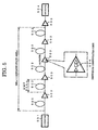
Fig. 5 is a block diagram showing a model of a transmission system
for simulating the embodiments of the present invention;
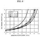
Fig. 6 is a graph showing repeater output power vs. eye opening
penalty characteristic for explaining improved points by the first to forth
embodiments of the present invention;
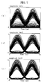
Figs. 7(a), 7(b) and 7(c) are graphs showing post-transmission eye
patterns at the repeater output power of +9dBm in Fig. 6 according to (a)
RZ modulation, (b) CS-RZ modulation and (c) chirp-giving CS-RZ
modulation, respectively;
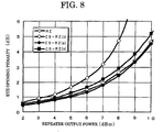
Fig. 8 is a graph showing repeater output power vs. eye opening
penalty characteristic with respect to a normal dispersion fiber for
explaining improved points in the present invention;
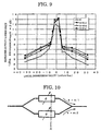
Fig. 9 is a graph showing local dispersion value vs. repeater output
upper limit for explaining improved points in the present invention;
Fig. 10 is a block diagram showing the configuration of a two-beam
interferometer type optical modulator;
Figs. 11(a), 11(b) and 11(c) are diagrams for explaining the operation
of the two-beam interferometer type optical modulator by phasor;
Figs. 12(a), 12(b) and 12(c) are cross section diagrams showing the
configuration of an LN optical modulator;
Fig. 13 is a block diagrams showing a conventional CS-RZ
modulation transmitter;
Fig. 14 is a diagrams for explaining the operation of an LN modulator
in a CS clock modulating section; and
Figs. 15(a), 15(b) and 15(c) are diagrams showing the vector trace of
modulated output light with respect to the CS-RZ modulation, to which
various prechirps are given.
BEST MODE FOR CARRYING OUT THE INVENTION
[First Embodiment]
Fig. 1 is a block diagram showing the configuration of an optical
transmitter according to the first embodiment of the present invention.
First, light at a wavelength of 1.55µm emitted from a semiconductor laser as
a light source 100 undergoes the NRZ modulation by a chirp-giving LN
modulator 103 at a data modulating section 101. The light then undergoes
the CS clock modulation by a push-pull type LN modulator 104 at a CS
clock modulating section 102. The chirp-giving LN modulator 103 has the
configuration depicted in Fig. 12(b).
In the conventional CS-RZ modulation, the data modulating section is
provided with the two-input push-pull type LN modulator 133 that is
capable of chirpless modulation. On the other hand, according to the
present invention, the LN modulator 103 applies the chirp differently from
the conventional method. Besides, while the two-input push-pull type LN
modulator 133 requires a pair of complementary drive signals to start
operations, the chirp-giving LN modulator 103 in general needs one input.
This brings side benefits that the line of the drive signal is simplified, and
the device can be produced at a lower cost.
Incidentally, according to the conventional CS-RZ moderation method,
the data modulating section 131 is driven by electrical signals in the NRZ
modulation format. Even though the NRZ modulation is adopted as a
modulation format for the data modulating section 131, definitive light
output turns out to be in the RZ modulation format by the CS clock
modulation. Meanwhile, the data modulating section 101 of the present
invention is not limited to adopting the NRZ modulation as its modulation
format, and the RZ modulation format is also available. That is, the LN
modulator 103 in the data modulating section 101 may be driven by
electrical signals in the RZ modulation format.
[Second Embodiment]
Fig. 2 is a block diagram showing the configuration of an optical
transmitter according to the second embodiment of the present invention.
In this embodiment, a data modulating section 201 is provided with an EA
modulator 203 differently from the data modulating section 101 in the first
embodiment. The letters EA stand for Electro-Absorption. This device
serves as an optical shutter, which makes a change in the band gap of an
optical semiconductor with applied electric field to take advantage of a
change in absorption edge wavelength caused thereby.
When the EA modulator 203 changes the amount of absorption by
applying electric field, generally, the refractive index also changes at the
same time. Accordingly, the light passing through the modulator 203
undergoes a phase modulation, namely, the chirp. The direction of the
chirp at the EA modulator 203 varies with reverse bias voltage
superimposed on the drive signal. Generally, it continuously shifts in a
counter- SPM direction when the bias voltage is small, and shifts in a SPM
direction when the bias voltage is large. The bias point is, however,
adjusted so that output signal light is favorably intensity-modulated, and
cannot be set arbitrarily. For the present, the direction of the chirp at
standard bias voltage in common EA modulators is opposite to that of SPM,
which is convenient for implementing the present invention in a
transmission line becoming a commonly used WDM communication fiber
with a relatively large dispersion value.
The EA modulator 203 is similar to the semiconductor laser used as
the light source 100 in composition and manufacturing process. Therefore,
they can be integrally manufactured together. Such unified modulator and
light source have already been in practical use, and make a big contribution
to reductions in cost and the miniaturization of optical transmitters. While
in the second embodiment, the integrated combination of the modulator 203
and light source 100 is not employed because of a high modulation rate of
40Gb/s and separate ones are used, it will be possible to use the integrated
ones in the configuration of the optical transmitter according to the present
invention.
Incidentally, the EA modulator 203 may also be driven by electrical
signals in the RZ modulation format as well as the NRZ modulation format.
[Third Embodiment]
Fig. 3 is a block diagram showing the configuration of an optical
transmitter according to the third embodiment of the present invention. In
the first and second embodiments, the push-pull type LN modulator 104 that
requires two electrical signal inputs is used as a chirpless optical modulator
in the clock modulating section 102. On the other hand, in this
embodiment, an LN modulator 304, which is capable of push-pull drive
with one electrical signal input, is employed. By virtue of this
construction, there is no need to coordinate the phases and amplitudes of a
pair of complementary drive signals, and reductions in cost can be realized.
The LN modulator 304 can perform push-pull drive with one drive
signal input since electric field generated by the input signal is applied to
two arms of the interferometer in opposite phases as shown in Fig. 12(c).
The two-input type LN modulator 104 used in the first and second
embodiments can carry out different phase modulations at the respective
arms with two input signals, and is capable of variable combinations of
modulations other than the push-pull drive. However, when the usage of
the modulator is limited to the push-pull drive which only requires opposite
phase modulations, the configuration of the device can be largely
simplified.
Although the one-input type chirpless modulator including an "X (Y)
axis-cut, Y (X) axis-propagation" substrate as shown in Fig. 12(c) has been
known, it has been barely commercially available because of difficulty in
manufacturing the LN substrate. Meanwhile, "Z axis-cut, X (Y)
axis-propagation" substrate as shown in Figs. 12(a) and 12(b) has been
mainly utilized. In addition, the one-input type chirpless modulator
including an "X (Y) axis-cut, Y (X) axis-propagation" substrate has not
been employed for generating CS clock signals.
The CS clock modulating section 302 provided with the one-input
type chirpless LN modulator 304 and a one-input type chirp-giving data
modulating section (e.g. the LN modulator 103 in Fig. 1 or the EA
modulator 203 in Figs. 2 and 3) makes the most simple combination and
requires one DATA signal and one clock signal (its frequency is a half of bit
rate frequency) as drive signals. This configuration saves points that need
adjustment, and is highly practical.
[Fourth Embodiment]
Fig. 4 is a block diagram showing the configuration of an optical
transmitter according to the fourth embodiment of the present invention.
This embodiment is characterized in that the device further includes an EA
modulator 403 that is driven by a clock signal of bit rate frequency for
setting the modulation to the RZ modulation format.
While in the first to third embodiments, a data electrical signal itself is
arranged in the RZ modulation format to adopt the RZ modulation as the
modulation format for the data modulating section, it is also possible to
separate roles and use the modulator 203 for data modulation and the
modulator 403 for clock modulation.
This construction solves the problem in the RZ modulation format that
it is rather difficult to realize an electric circuit because the waveform of an
electrical signal in the RZ format is not vertically symmetrical in the
direction of amplitude and a wider band is used as compared to the NRZ
modulation format. Moreover, freedoms of choice of pulse width, pulse
form, etc. are broadened by separately providing the modulator 403 for
setting the modulation to the RZ modulation format. Additionally, when
employing the modulator 403 that exclusively conducts RZ modulation
methodizing, the chirp in a direction opposite to SPM may be given by the
modulator.
Next, a description will be given of the extent of improvement in
transmission characteristics brought by the improved CS-RZ modulation
signals obtained in the first to fourth embodiments.
Fig. 5 is a block diagram showing a model of a transmission system
for simulating the embodiments of the present invention. In the following
simulation, the present invention is applied to an optical transmission
system with a bit rate of 40Gb/s, a signal light wavelength of 1.55µm, and a
transmission distance of 80km × 6 repeater spans. As for the transmission
line in the system, a dispersion-arranged transmission line is employed. In
the dispersion-arranged transmission line, SMF is used as line fibers 502,
and a dispersion compensating fiber 505 is used as a dispersion
compensating device in a repeater 503. With this construction, while the
local chromatic dispersion in the signal band is non zero, the amount of
cumulative chromatic dispersion from a transmitter 501 to a receiver 504 is
approximately zero. The transmission line runs the length of SMF-80km ×
6 repeater spans: 480km. The input power to the dispersion compensating
fiber 505 in the repeater 503 is set to -10dB lower than SMF input power
(horizontal axis).
In the following, a description will be give of the effect of the present
invention based on the result of a computer simulation by which the
SPM-GVD phenomenon can be faithfully demonstrated. Fig. 6 is a graph
showing experimental results of the relationship between repeater output
and waveform distortion in the respective modulation methods. The
horizontal axis is a repeater output power (dBm) scale, the vertical axis is
an area scale for eye opening immediately after a transmitter as a reference.
In Fig. 6, CS-RZ (0), CS-RZ (p), and CS- RZ (m) indicate the types of
modulation in terms of chirp. CS-RZ (0) represents chirpless modulation
(prior art), CS-RZ (p) represents modulation with the chirp in a counter-SPM
direction, and CS-RZ (m) represents modulation with the chirp in a
SPM direction.
It is observed that the eye is getting more deformed due to the
SPM-GVD degradation as the repeater output power gets high. In the view
of the differences among modulation methods, the method being most apt to
induce the degradation is the RZ modulation, followed by the CS- RZ (m)
modulation, CS-RZ (0) modulation, and CS-RZ (p) modulation improved by
the present invention in this order.
Figs. 7(a), 7(b) and 7(c) are graphs showing eye patterns at the
repeater output power of +9dBm with respect to the RZ modulation, CS-RZ
(0) modulation and CS-RZ (p) modulation, respectively. Extensive
improvement is achieved by adopting the CS-RZ modulation instead of the
RZ modulation. Moreover, noise at 0 level is improved by performing the
chirp in a counter- SPM direction at the data modulating section. Provided
that tolerable eye opening penalty is 2dB, the maximum output power value
is improved by approximately 1.6dB when the RZ modulation is replaced by
the CS-RZ modulation. In addition, with the chirp-giving CS-RZ
modulation, the maximum output power value is further improved by
approximately 0.4dB. That is, when adopting the chirp-giving CS-RZ
modulation instead of the RZ modulation, the maximum output power value
is improved by approximately 2dB, which represents a transmission loss of
10km, and an increase of 12.5% in terms of transmission distance
percentage.
For the purpose of confirmation, it is also given of the result in the
case of the chirp in a SPM direction. The result shows that the degradation
is more easily induced in this case than in the case of the chirpless
modulation.
Fig. 8 is a graph as with Fig. 6, but for showing simulation results
when the polarity of fiber dispersion is reversed. There is no such fiber in
a practical sense. However, it is possible to perform a thought experiment
by a simulation. In comparison with Fig. 6, there is less degradation in
every modulation method. Accordingly, less improvement results are
achieved when replacing the CS-RZ modulation with the chirp-giving
CS-RZ modulation. Herewith, it turns out that the present invention is
especially effective in the case where the dispersion of a transmission fiber
producing nonlinear effect is the abnormal dispersion. Incidentally, the
chirp in a counter- SPM direction displays superiority also in this case.
As is described above, the optimum direction of the chirp is opposite
to the direction of SPM at a local dispersion value of ± 16ps/ nm/ km.
Fig. 9 is a graph showing simulation results at another local dispersion
value. In Fig. 9, CS-RZ (0), CS-RZ (p), and CS- RZ (m) indicate the types
of modulation in terms of chirp. CS-RZ (0) represents chirpless
modulation (prior art), CS-RZ (p) represents modulation with the chirp in a
counter- SPM direction, and CS-RZ (m) represents modulation with the
chirp in a SPM direction.
Fig. 9 shows that the improvement factor of the CS-RZ modulation
over the RZ modulation is especially extensive in the range where the
absolute value of the local dispersion exceeds 6ps/ nm/ km. Additionally,
the CS-RZ modulation with the chirp in a counter- SPM direction displays
best results almost everywhere in the range.
While preferred embodiments of the present invention have been
described, such description is for illustrative purpose only, and it is to be
understood that changes and variations may be made without departing from
the spirit or scope of the invention.
For example, any type of optical intensity modulator which applies the
prechirp in a counter-SPM direction may be employed for the data
modulating section as well as the chirp-giving LN modulator or EA
modulator. It is also possible to use the combination of modulators, one
for performing intensity modulation, and the other for phase modulation.
Besides, a carrier may be prechirped at the light source through a direct
modulation technique for producing the prechirp by superimposing a clock
frequency signal on the drive current of the semiconductor laser light
source.
While the one-input or two-input driven push-pull type LN modulator
is used for the CS clock modulating section in the above embodiments, any
modulator configuration, in which the phase is reversed with respect to each
bit without chirp, may be employed.
In the above embodiments, LN (LiNbO3) is used as material for
realizing the two-beam interferometer type modulator. However, the
modulator is not limited to this structure, and may be realized by building
up a waveguide and a modulator on an optical semiconductor substrate.
This example has been disclosed in the report, C Rolland et al., "10Gbit/ s,
1.56µm multiquantum well InP/ InGaAsP Mach-Zehnder optical modulator",
Electron. Lett., p. 471, 1993. In addition, a two-beam interferometer may
be combined with a phase modulator by bulk material.
Besides, while the CS clock modulation is carried out after the data
modulation in the above embodiments, it is natural that the same result can
be obtained if the order is reversed.
The waveform of the drive signal for the CS clock modulating section
is not limited to absolute sinusoidal wave. Essential effect is not ruined
with distorted sinusoidal wave or rectangular wave if only the signal is
provided with a half of bit rate frequency.
While, in the above embodiments, one wavelength is used in
transmission, the essential effect of the present invention is not ruined by
using the wavelength-division multiplexing together.
Furthermore, while SMF is employed as a line fiber in the above
embodiments, the essential effect of the present invention is not ruined with
a line fiber having different chromatic dispersion characteristics.
INDUSTRIAL APPLICABILITY
As set forth hereinabove, in accordance with the present invention, it
is possible to obtain modulation signals with higher SPM-GVD resistance as
compared to the conventional CS-RZ modulation, thus enabling an increase
in transmission distance and an improvement in code error rate in optical
transmission systems whose performance is constrained by SPM-GVD.