EP1304703A1 - Antiscattering grid and a method of manufacturing such a grid - Google Patents
Antiscattering grid and a method of manufacturing such a grid Download PDFInfo
- Publication number
- EP1304703A1 EP1304703A1 EP02257225A EP02257225A EP1304703A1 EP 1304703 A1 EP1304703 A1 EP 1304703A1 EP 02257225 A EP02257225 A EP 02257225A EP 02257225 A EP02257225 A EP 02257225A EP 1304703 A1 EP1304703 A1 EP 1304703A1
- Authority
- EP
- European Patent Office
- Prior art keywords
- grid
- substrate
- partitions
- radiation
- cells
- Prior art date
- Legal status (The legal status is an assumption and is not a legal conclusion. Google has not performed a legal analysis and makes no representation as to the accuracy of the status listed.)
- Withdrawn
Links
Images


Classifications
-
- G—PHYSICS
- G21—NUCLEAR PHYSICS; NUCLEAR ENGINEERING
- G21K—HANDLING OF PARTICLES OR IONISING RADIATION NOT OTHERWISE PROVIDED FOR; IRRADIATION DEVICES; GAMMA RAY OR X-RAY MICROSCOPES
- G21K1/00—Arrangements for handling particles or ionising radiation, e.g. focusing or moderating
- G21K1/02—Arrangements for handling particles or ionising radiation, e.g. focusing or moderating using diaphragms, collimators
- G21K1/025—Arrangements for handling particles or ionising radiation, e.g. focusing or moderating using diaphragms, collimators using multiple collimators, e.g. Bucky screens; other devices for eliminating undesired or dispersed radiation
-
- B—PERFORMING OPERATIONS; TRANSPORTING
- B33—ADDITIVE MANUFACTURING TECHNOLOGY
- B33Y—ADDITIVE MANUFACTURING, i.e. MANUFACTURING OF THREE-DIMENSIONAL [3D] OBJECTS BY ADDITIVE DEPOSITION, ADDITIVE AGGLOMERATION OR ADDITIVE LAYERING, e.g. BY 3D PRINTING, STEREOLITHOGRAPHY OR SELECTIVE LASER SINTERING
- B33Y80/00—Products made by additive manufacturing
Definitions
- the invention relates to antiscattering grids and particularly to antiscattering grids used in X-ray imaging.
- a radiology imaging apparatus may comprise an X-ray source and an image receiver between which the object, of which it is wished to produce an image, is positioned.
- the beam emitted by the source passes through the object before reaching the detector. It is partly absorbed by the internal structure of the object so that the intensity of the beam received by the detector is attenuated.
- the overall attenuation of the beam after having passed through the object is directly related to the absorption distribution in the object.
- the image receiver may comprise an optoelectronic detector or enhancing film/screen pair sensitive to the intensity of the radiation.
- the image generated by the receiver corresponds in principle to the distribution of the overall attenuations of the rays due to having passed through the internal structures of the object.
- One part of the radiation emitted by the source is absorbed by the internal structure of the object and the other part is either transmitted (primary or direct radiation) or scattered (secondary or scattered radiation).
- the presence of scattered radiation results in the contrast of the image obtained being degraded and the signal/noise ratio being reduced.
- One solution to this problem comprises interposing one or more "antiscattering" grids between the object to be X-rayed and the image receiver.
- This grid is usually formed by a series of parallel plates made of a material that absorbs the X-rays.
- a grid identified as a "focused” grid using the terminology defined by the CEI 60627 standard relating to "X-ray imaging diagnostic equipment - characteristics of the antiscattering grids for general use and for mammography"
- all the planes of the plates intersect along the same straight line passing through the focal point of the radiation emitted by the source.
- a antiscattering grid may comprise a series of oriented parallel plates made of a material which strongly absorbs the X-rays, for example, lead, and are held together between inter-plate members made of a material more transparent to X-rays than the plates, such as, for example, aluminum or cellulose fibers (paper or wood).
- a disadvantage for such a grid is that the grid is unable to reduce the degree of radiation scattered in a direction parallel to the plane of the plates.
- the crossed grids allow two-dimensional filtering to be obtained and thus further reduce the solid angle with which a point on the receiver sees the object.
- One structural arrangement is two-dimensional filtering comprising superposing one-dimensional grids.
- US 5,307,394 describe an antiscattering device comprising the superposition of several grids.
- Each grid has parallel absorbent plates separated by openings, the plates being positioned at an angle of between 0 and 89.9° with respect to the central beam perpendicular to the plane of the receiver.
- the grids have a thickness such that the ratio of the thickness of the grid to the distance between the plates is greater than 1. This arrangement provides filtering of the rays whose angle of incidence is high.
- Another structural arrangement comprises producing two-dimensional grids directly in a one-piece support.
- US 5,389,473 describes a method of manufacturing an antiscattering grid, comprising producing a grid from a glass plate, making openings in the plate by photoetching and chemical etching (for example using hydrofluoric acid). Such a method results in an array of cells separated by partitions being formed. The partitions are then covered with a layer of material that absorbs the X-rays.
- WO 94/17533 describes an antiscattering grid comprising a lattice formed in a glass plate, the lattice comprising cells separated by partitions.
- the partitions are covered with a layer of absorbent material, not only inside the cells but also along their edges corresponding to the upper and lower surfaces of the glass plate.
- US 5,606,589 describe an antiscattering grid comprising thin metal sheets micro-etched to form a lattice. The sheets are superposed so as to form a focused grid. The sheets are held stacked together by adhesive bonding.
- US 5,814,235 describes a method of manufacturing such a grid.
- the method comprises forming, by photoetching in a metal foil, a lattice structure comprising cells separated by segments extending in transverse directions.
- the foils are then individually immersed in a bath of adhesive.
- the foils are then stacked on top of each other so as to align the segments in order to form partitions between the cells and then clamped together in position. This method makes it possible in particular to obtain strong grids.
- a disadvantage with the antiscattering grids in general is that they mask part of the image receiver and leave their impression on the image obtained.
- a solution to this problem comprises slightly shifting the grid during image acquisition.
- the image obtained comprises the superposition of images, for which the grid lies in different positions.
- An embodiment of the present invention provides a grid that is two dimensional for limiting the filtering of the direct radiation.
- An embodiment provides an antiscattering grid for radiation, particularly for an X-ray imaging apparatus, of the type comprising a substrate having a plurality of metallized partitions that together define a plurality of cells distributed over the substrate. The partitions allow passage of radiation emitted from a source lying in line with the grid, and absorbing the radiation not coming directly from this source.
- the substrate is made of a polymer material. The polymer material is less absorbent of the radiation and therefore permits more of the direct radiation to pass through. This feature permits in particular the reduction of the radiation doses administered to the object.
- the external surfaces of the substrate are not metallized, thereby allowing some of the direct radiation to pass through the substrate. This makes it possible to further increase the quality of the image without increasing the radiation doses administered to the object.
- the gird has less strict dimensioning constraints while still exhibiting superior performance.
- An embodiment is a method for the manufacture of such grids.
- An embodiment is a method of manufacturing an antiscattering grid comprising a substrate made of a polymer material, in which the substrate is formed by radiation curing of a monomer sensitive to the radiation.
- the method may comprise, for example, laser photolithography (and in particular the technique known as "stereolithography") or X-ray lithography.
- the method of manufacturing an antiscattering grid may comprise: (a) forming, for example, by stereo-lithography, a substrate having a plurality of partitions which together define a plurality of cells distributed over the said substrate; and (b) depositing a layer of metal on the surface of the substrate.
- the substrate of the grid may be formed from a wide range of low-density materials. It may, for example, comprise an epoxy resin or an acrylic resin. These materials have a density and an atomic number that are low enough to have low radiation absorption, particularly for X-rays.
- a grid may have cells with openings of about 200 ⁇ m (micrometers) to about 300 ⁇ m and comprising partitions having a thickness of about 50 ⁇ m to about 100 ⁇ m.
- Figure 1 shows schematically the principle of operation of an antiscattering grid 1 mounted in a radiology apparatus.
- the grid 1 is positioned in front of a detector screen 42 so that the radiation source 44 is located at the focal point O of the grid 1.
- One part of the direct radiation D emitted by the source 44 passes through an object 46, the image of which it is wished to obtain, without undergoing distortion.
- Another part d of the radiation is scattered by the object 46 so that it strikes the grid at an angle ⁇ to the focusing direction of the grid 1. Since the internal partitions of the grid 1 are focused, they absorb the scattered radiation d.
- Figure 2 shows more specifically the paths of the radiation, during image acquisition, through an antiscattering grid of an embodiment.
- the grid comprises a substrate 2 made of a polymer material, comprising partitions 8 which define cells 12.
- the internal walls of the cells 12 are covered with a metal layer 14.
- a part D1 of the direct radiation D passes through the grid 1 via the substrate 2, while another part D2 passes through the grid 1 via the cells 12. Because of the low density of the polymer of which the substrate 2 is formed, the radiation D1 undergoes little attenuation.
- the internal walls of the cells 12 are covered with a metal layer 14 that absorbs the scattered radiation d striking the grid 1 at too great an angle ⁇ to the focusing direction of one of the cells 12.
- An embodiment is directed to two types of grids.
- a first type of which the grids have an opening x of about 200 ⁇ m to about 300 ⁇ m and comprise partitions having a thickness e of about 50 ⁇ m to about 100 ⁇ m; and a second type of finer grids with a pitch of about 50 ⁇ m to about 100 ⁇ m and comprising partitions having a thickness e of about 20 ⁇ m to about 50 ⁇ m.
- Grids for a radiology apparatus may have a ratio of the thickness of the grid to the distance between the partitions of between 3 and 5.
- the disclosed embodiments makes it possible to obtain grids having ratios greater than 8, whether the grids are linear or crossed. This feature ensures filtering of the rays whose angle of incidence deviates, even slightly, from the direction of direct radiation and consequently results in grids having extremely high rejection properties.
- Figure 3 shows the overall shape of a substrate 2 of a focused antiscattering grid according to one embodiment.
- the substrate is in the form of a substantially planar element, of thickness e, having two principal faces, an upper face 4 and a lower face 6.
- the substrate is composed of intersecting partitions 8 defining cells 12 passing through the substrate from one of its principal faces to the other.
- the substrate 2 is "focused", that is to say by definition, the planes containing the partitions 8 between the cells 12 all have the same focal point O, as shown in Figure 4.
- the cells 12 are square in shape and define a quasi-periodic pattern (or instead one in which the pitch or the period varies continuously).
- the pitch may correspond to the distance between two successive parallel partitions.
- cells having various polyhedral shapes are possible.
- cells preferably have the shape of a parallelogram.
- a parallelogram is that category of shapes which minimizes as far as possible the surface area occupied by the partitions and therefore makes it possible to minimize the absorption of the grid.
- partitions separating the cells are not necessarily aligned. They may be parallel and offset from one cell to the next. This gives the grid some advantages. In particular, this feature makes it possible to minimize the generation of impressions of the partitions on the image obtained when these impressions are approximately parallel to the direction of displacement of the grid.
- the substrate 2 is designed by computer-aided design.
- the geometrical features of the substrate 2 are defined according to the desired properties of the grid. From these geometrical features, a polyhedral surface model is generated which can be exported to the STL (standing for stereo-lithography) format. This format allows an object to be described in the form of a polyhedron having triangular facets.
- the sections of the substrate 2 to be produced by successive cutting of parallel horizontal planes are defined.
- the distance between each section corresponds to the thickness of a layer.
- Figure 5 shows a first step in the manufacture of a substrate by stereolithography.
- a precursor fluid 22 for example photosensitive liquid acrylate or epoxy resins
- a tank 24 kept at a high pressure (between 300 kPa and 7000 kPa) by means of a pump device 26 connected to the tank 24 and in communication with the precursor fluid 22.
- the tank 24 is closed in its upper part by a window 28 (made of quartz, sapphire or silica).
- Figure 5 shows a platform 34, the principal surface of which is parallel to the free surface of the fluid 22 and is mounted on an elevator (not shown) which can be translationally actuated perpendicular to the plane of the platform 34.
- Figure 5 shows a source 32 emitting a beam through a lens 36 to an arrangement of mirrors 38.
- the source 32 is, for example, an ultraviolet laser source.
- the mirrors 38 are used to deflect the beam emitted by the source 32 onto the free surface of the precursor fluid 22.
- the mirrors are positionally controlled by a computer so as to perform a point-by-point scan of the layer of fluid 22 close to its free surface.
- the ultraviolet radiation emitted by the source 32 causes local curing of the precursor fluid 22.
- the mirrors 38 are controlled so that the beam draws on the surface of the fluid a pattern corresponding to the lower surface of the substrate 2.
- the elevator is actuated in order to lower the platform 34 supporting the cured layer by a height corresponding to the thickness of one layer (the thickness of a layer is determined by the level of viscosity of the precursor fluid chosen - it is generally less than one-tenth of a millimeter).
- the source again draws a new pattern in order to create a second layer on the first layer.
- Each cured layer is in the form of a lattice comprising segments defining openings.
- the layers are produced in succession so that the segments of two adjacent layers are superposed, thus forming the partitions of the cells of the substrate.
- the final substrate obtained is a one-piece substrate.
- Figure 6 shows an intermediate step during which a layer 52 of polymer is produced by stereo-lithography on that part 54 of the substrate that has already been produced.
- the final substrate 2 obtained is a one-piece substrate.
- the precursor fluid 22 contained in the tank 24 that has not reacted is drained off.
- the relative positions and dimensions of the openings and of the segments vary progressively from one layer to the next. In this way, it is possible to construct a substrate 2 having focused cells 12 for the purpose of obtaining a focused grid.
- the surface of the substrate 2 is metallized, by a chemical vapor deposition (CVD) process.
- CVD chemical vapor deposition
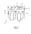
- Figure 7 Such a method is used to obtain a metal layer 14 having a thickness of the order of a few ⁇ m.
- the absorbent metals preferably used are gold (in the form of a layer from 2 ⁇ m to 5 ⁇ m in thickness), copper (in the form of a layer from about 10 ⁇ m to about 20 ⁇ m in thickness), tantalum (in the form of a layer from about 2 ⁇ m to about 10 ⁇ m in thickness) or possibly lead. These materials may be used by themselves, in combination or in association with other materials.
- PVD physical vapor deposition
- electrolysis electrolysis
- a third step those parts of the metal layer provided on or covering the upper surface 4 and the lower surface 6 of the substrate are removed.
- the metal layer can be removed by abrasion.
- the metal layer can be removed by plasma etching.
- the reactor may be of type used in the manufacture of micro electro mechanical systems (MEMS) or semiconductor integrated circuits.
- MEMS micro electro mechanical systems
- a plasma reactor of this type is available from Alcatel Micro Machining Systems (MMS) or Plasma Etch Inc.
- Plasma etching occurs in a vacuum and uses radio frequency energy to create plasma. The ions of the plasma react with the metallic layer that is to be removed.
- simple dry plasma etching may be used.
- gas contained in the reactor forms a simple plasma.
- the particle of metal located on the exposed surface of the metallic layer is removed by the impact of the ions contained in the plasma.
- plasma etching in the presence of active gas may be used.
- a reactive gas for example, SF 6, is introduced into the plasma so as to produce a combined physical and chemical etching.
- laser ablation may be used.
- the metallic layer is exposed to a focused radiation beam provided by a laser source.
- Laser ablation provides mechanical etching of the particles of metal.
- the laser source may a laser emitting in the ultraviolet band, such as Excimer laser sources.
- the laser source is controlled so as to sweep over the surface of the grid.
- the size of the laser spot generated by the radiation beam depends on the power of the source and the ablation threshold of the metal to be removed.
- the duration of the ablation process depends on the spot size, the pulse frequency of the laser source (in the case of a pulsed laser source), the thickness of the metal layer to be removed and the area of surface to be treated.
- the upper and lower surfaces can be de-coated one at a time. However, it is possible to de-coat both surfaces simultaneously using two laser source or one laser source and a beam splitter.
- Plasma etching or laser ablation provides a substantially uniform removal of the metal layer from desired surfaces of the grid and provides a substantially clean cut of the metal layer at the edges of the cell walls.
- a substantially uniform removal and cut of the metal layer may maintain a high transmission of the radiation through the grid.
- the antiscattering grid is made homogeneous and the attenuation is thus distributed uniformly, in order to reduce any artifacts that it generates on the images obtained. This is mainly so in the case of grids having a thickness of less than about 1 mm, the attenuation of which is negligible.
Landscapes
- Physics & Mathematics (AREA)
- Spectroscopy & Molecular Physics (AREA)
- Engineering & Computer Science (AREA)
- General Engineering & Computer Science (AREA)
- High Energy & Nuclear Physics (AREA)
- Measurement Of Radiation (AREA)
- Apparatus For Radiation Diagnosis (AREA)
Abstract
An antiscattering grid for an X-ray imaging apparatus of the type comprising a
substrate (2) having a plurality of metallized partitions (8) that together define
a plurality of cells (12) distributed over the substrate (2). The partitions (8)
allow passage of the X-rays (D) emitted from a source lying in line with the
grid, and absorbing the X-rays not coming directly from this source. The
substrate (2) is made of a polymer material that may be formed by radiation
curing of a monomer sensitive to this radiation. The substrate may be
substantially planar and the partitions may be oriented to form a focused grid.
Description
- The invention relates to antiscattering grids and particularly to antiscattering grids used in X-ray imaging. A radiology imaging apparatus may comprise an X-ray source and an image receiver between which the object, of which it is wished to produce an image, is positioned. The beam emitted by the source passes through the object before reaching the detector. It is partly absorbed by the internal structure of the object so that the intensity of the beam received by the detector is attenuated. The overall attenuation of the beam after having passed through the object is directly related to the absorption distribution in the object.
- The image receiver may comprise an optoelectronic detector or enhancing film/screen pair sensitive to the intensity of the radiation. The image generated by the receiver corresponds in principle to the distribution of the overall attenuations of the rays due to having passed through the internal structures of the object.
- One part of the radiation emitted by the source is absorbed by the internal structure of the object and the other part is either transmitted (primary or direct radiation) or scattered (secondary or scattered radiation). The presence of scattered radiation results in the contrast of the image obtained being degraded and the signal/noise ratio being reduced.
- One solution to this problem comprises interposing one or more "antiscattering" grids between the object to be X-rayed and the image receiver. This grid is usually formed by a series of parallel plates made of a material that absorbs the X-rays. In a grid identified as a "focused" grid (using the terminology defined by the CEI 60627 standard relating to "X-ray imaging diagnostic equipment - characteristics of the antiscattering grids for general use and for mammography"), all the planes of the plates intersect along the same straight line passing through the focal point of the radiation emitted by the source.
- A antiscattering grid may comprise a series of oriented parallel plates made of a material which strongly absorbs the X-rays, for example, lead, and are held together between inter-plate members made of a material more transparent to X-rays than the plates, such as, for example, aluminum or cellulose fibers (paper or wood). A disadvantage for such a grid is that the grid is unable to reduce the degree of radiation scattered in a direction parallel to the plane of the plates. Crossed grids having two series of absorbent plates, in which the two plates are positioned perpendicular to each other, reduce this disadvantage. The crossed grids allow two-dimensional filtering to be obtained and thus further reduce the solid angle with which a point on the receiver sees the object.
- However, the presence of inter-plate members between the plates reduces the transmission of the direct radiation through the grid. Consequently, the X-ray dose needed to obtain an image of good quality must be increased (particularly in mammography).
- There are several structural arrangements for obtaining grids without inter-plate members. One structural arrangement is two-dimensional filtering comprising superposing one-dimensional grids. US 5,307,394 describe an antiscattering device comprising the superposition of several grids. Each grid has parallel absorbent plates separated by openings, the plates being positioned at an angle of between 0 and 89.9° with respect to the central beam perpendicular to the plane of the receiver. The grids have a thickness such that the ratio of the thickness of the grid to the distance between the plates is greater than 1. This arrangement provides filtering of the rays whose angle of incidence is high.
- Another structural arrangement comprises producing two-dimensional grids directly in a one-piece support. US 5,389,473 describes a method of manufacturing an antiscattering grid, comprising producing a grid from a glass plate, making openings in the plate by photoetching and chemical etching (for example using hydrofluoric acid). Such a method results in an array of cells separated by partitions being formed. The partitions are then covered with a layer of material that absorbs the X-rays.
- WO 94/17533 describes an antiscattering grid comprising a lattice formed in a glass plate, the lattice comprising cells separated by partitions. The partitions are covered with a layer of absorbent material, not only inside the cells but also along their edges corresponding to the upper and lower surfaces of the glass plate.
- In the field of mammography, another type of two-dimensional grid has been developed. US 5,606,589 describe an antiscattering grid comprising thin metal sheets micro-etched to form a lattice. The sheets are superposed so as to form a focused grid. The sheets are held stacked together by adhesive bonding.
- US 5,814,235 describes a method of manufacturing such a grid. The method comprises forming, by photoetching in a metal foil, a lattice structure comprising cells separated by segments extending in transverse directions. The foils are then individually immersed in a bath of adhesive. The foils are then stacked on top of each other so as to align the segments in order to form partitions between the cells and then clamped together in position. This method makes it possible in particular to obtain strong grids.
- US 6,075,840 generalizes this type of grid for applications other than mammography.
- The disadvantage with the above methods is that they are based on the chemical etching of layers of materials and consequently result in a significant loss of material, and hence high costs.
- Moreover, a disadvantage with the antiscattering grids in general is that they mask part of the image receiver and leave their impression on the image obtained. A solution to this problem comprises slightly shifting the grid during image acquisition. Thus, the image obtained comprises the superposition of images, for which the grid lies in different positions.
- In certain cases, it is possible to translate the grid only in a single direction (in particular in mammography, in which the direction of displacement is parallel to the patient's thoracic cage). In this case, the impressions of the segments or of the partitions which are positioned parallel to the direction of displacement of the grid remain on the image obtained. US 5,970,118 describes an antiscattering grid formed in a glass plate in which the partitions of the cells are not parallel to the side of the grid parallel to the direction of displacement of the latter. For example, the grid may comprise cells having a square shape and oriented at 35° with respect to an edge of the grid parallel to the direction of displacement.
- An embodiment of the present invention provides a grid that is two dimensional for limiting the filtering of the direct radiation. An embodiment provides an antiscattering grid for radiation, particularly for an X-ray imaging apparatus, of the type comprising a substrate having a plurality of metallized partitions that together define a plurality of cells distributed over the substrate. The partitions allow passage of radiation emitted from a source lying in line with the grid, and absorbing the radiation not coming directly from this source. In an embodiment of the invention the substrate is made of a polymer material. The polymer material is less absorbent of the radiation and therefore permits more of the direct radiation to pass through. This feature permits in particular the reduction of the radiation doses administered to the object.
- In an embodiment, the external surfaces of the substrate are not metallized, thereby allowing some of the direct radiation to pass through the substrate. This makes it possible to further increase the quality of the image without increasing the radiation doses administered to the object.
- In an embodiment as the substrate is less absorbent of radiation the gird has less strict dimensioning constraints while still exhibiting superior performance.
- One embodiment is a method for the manufacture of such grids. An embodiment is a method of manufacturing an antiscattering grid comprising a substrate made of a polymer material, in which the substrate is formed by radiation curing of a monomer sensitive to the radiation. The method may comprise, for example, laser photolithography (and in particular the technique known as "stereolithography") or X-ray lithography.
- The method of manufacturing an antiscattering grid may comprise: (a) forming, for example, by stereo-lithography, a substrate having a plurality of partitions which together define a plurality of cells distributed over the said substrate; and (b) depositing a layer of metal on the surface of the substrate. In an embodiment of the method, the substrate of the grid may be formed from a wide range of low-density materials. It may, for example, comprise an epoxy resin or an acrylic resin. These materials have a density and an atomic number that are low enough to have low radiation absorption, particularly for X-rays.
- Forming the substrate by, for example, stereo-lithography, allows small cells to be obtained. In particular, in an embodiment of the invention, there may be two broad types of grids. A grid may have cells with openings of about 200 µm (micrometers) to about 300 µm and comprising partitions having a thickness of about 50 µm to about 100 µm. A grid having a pitch of about 50 µm to about 100 µm and comprising partitions having a thickness of about 20 µm to about 50 µm.
- The invention will now be described in greater detail, by way of example, with reference to the drawings, in which:-
- Figure 1 is a schematic representation the principles of operation of an antiscattering grid positioned in a camera of a radiology apparatus;
- Figure 2 is a sectional representation of a grid of an embodiment and illustrating the paths followed by the direct and scattered rays through the grid;
- Figure 3 is a schematic representation of a substrate comprising an antiscattering grid according to an embodiment;
- Figure 4 is a cross-sectional representation, with exaggerated proportions, of a substrate formed by an embodiment of the method for manufacturing the grid;
- Figure 5 shows schematically a first step in the manufacture of the grid, this step corresponding to the production of the substrate shown in Figure 4 by stereo-lithography;
- Figure 6 shows schematically an intermediate step in the production of the substrate, during which a layer of polymer is produced by stereo-lithography; and
- Figure 7 is a detailed diagram of the grid obtained.
-
- Figure 1 shows schematically the principle of operation of an
antiscattering grid 1 mounted in a radiology apparatus. Thegrid 1 is positioned in front of adetector screen 42 so that theradiation source 44 is located at the focal point O of thegrid 1. One part of the direct radiation D emitted by thesource 44 passes through anobject 46, the image of which it is wished to obtain, without undergoing distortion. Another part d of the radiation is scattered by theobject 46 so that it strikes the grid at an angle α to the focusing direction of thegrid 1. Since the internal partitions of thegrid 1 are focused, they absorb the scattered radiation d. - Figure 2 shows more specifically the paths of the radiation, during image acquisition, through an antiscattering grid of an embodiment. The grid comprises a
substrate 2 made of a polymer material, comprisingpartitions 8 which definecells 12. The internal walls of thecells 12 are covered with ametal layer 14. A part D1 of the direct radiation D passes through thegrid 1 via thesubstrate 2, while another part D2 passes through thegrid 1 via thecells 12. Because of the low density of the polymer of which thesubstrate 2 is formed, the radiation D1 undergoes little attenuation. - The internal walls of the
cells 12 are covered with ametal layer 14 that absorbs the scattered radiation d striking thegrid 1 at too great an angle α to the focusing direction of one of thecells 12. - An embodiment is directed to two types of grids. A first type, of which the grids have an opening x of about 200 µm to about 300 µm and comprise partitions having a thickness e of about 50 µm to about 100 µm; and a second type of finer grids with a pitch of about 50 µm to about 100 µm and comprising partitions having a thickness e of about 20µm to about 50 µm.
- Grids for a radiology apparatus, for example, in mammography, may have a ratio of the thickness of the grid to the distance between the partitions of between 3 and 5. The disclosed embodiments makes it possible to obtain grids having ratios greater than 8, whether the grids are linear or crossed. This feature ensures filtering of the rays whose angle of incidence deviates, even slightly, from the direction of direct radiation and consequently results in grids having extremely high rejection properties.
- In the case of grids of the first type mentioned above, a grid thickness e of greater than about 1.6 mm or about 2.4 mm, and less than about 3 mm, is obtained (should the ratio reach 10). In the case of grids of the second type, a grid thickness e of greater than about 0.4 mm or about 0.8 mm, and less than about 1 mm, is obtained (should the ratio reach 10).
- It may be advantageous to choose to manufacture a grid having a pitch equal to the period of the digital detector of the camera. This feature makes it possible to eliminate the gain modulations introduced by the grid and prevent a deflection generated by the superposition of the grid and of the detector from being obtained.
- Figure 3 shows the overall shape of a
substrate 2 of a focused antiscattering grid according to one embodiment. The substrate is in the form of a substantially planar element, of thickness e, having two principal faces, an upper face 4 and alower face 6. The substrate is composed of intersectingpartitions 8 definingcells 12 passing through the substrate from one of its principal faces to the other. Thesubstrate 2 is "focused", that is to say by definition, the planes containing thepartitions 8 between thecells 12 all have the same focal point O, as shown in Figure 4. - In Figure 3, the
cells 12 are square in shape and define a quasi-periodic pattern (or instead one in which the pitch or the period varies continuously). The pitch may correspond to the distance between two successive parallel partitions. - Cells having various polyhedral shapes are possible. However, in an embodiment cells preferably have the shape of a parallelogram. A parallelogram is that category of shapes which minimizes as far as possible the surface area occupied by the partitions and therefore makes it possible to minimize the absorption of the grid.
- It will also be understood that the partitions separating the cells are not necessarily aligned. They may be parallel and offset from one cell to the next. This gives the grid some advantages. In particular, this feature makes it possible to minimize the generation of impressions of the partitions on the image obtained when these impressions are approximately parallel to the direction of displacement of the grid.
- One embodiment of a substrate is described as follows. The
substrate 2 is designed by computer-aided design. The geometrical features of thesubstrate 2 are defined according to the desired properties of the grid. From these geometrical features, a polyhedral surface model is generated which can be exported to the STL (standing for stereo-lithography) format. This format allows an object to be described in the form of a polyhedron having triangular facets. - Next, the sections of the
substrate 2 to be produced by successive cutting of parallel horizontal planes are defined. The distance between each section corresponds to the thickness of a layer. - Figure 5 shows a first step in the manufacture of a substrate by stereolithography. A precursor fluid 22 (for example photosensitive liquid acrylate or epoxy resins) is contained in a
tank 24 kept at a high pressure (between 300 kPa and 7000 kPa) by means of apump device 26 connected to thetank 24 and in communication with theprecursor fluid 22. Thetank 24 is closed in its upper part by a window 28 (made of quartz, sapphire or silica). - Figure 5 shows a
platform 34, the principal surface of which is parallel to the free surface of the fluid 22 and is mounted on an elevator (not shown) which can be translationally actuated perpendicular to the plane of theplatform 34. Figure 5 shows asource 32 emitting a beam through alens 36 to an arrangement ofmirrors 38. Thesource 32 is, for example, an ultraviolet laser source. Themirrors 38 are used to deflect the beam emitted by thesource 32 onto the free surface of theprecursor fluid 22. The mirrors are positionally controlled by a computer so as to perform a point-by-point scan of the layer offluid 22 close to its free surface. - The ultraviolet radiation emitted by the
source 32 causes local curing of theprecursor fluid 22. Themirrors 38 are controlled so that the beam draws on the surface of the fluid a pattern corresponding to the lower surface of thesubstrate 2. When a first layer of polymer has been thus produced, the elevator is actuated in order to lower theplatform 34 supporting the cured layer by a height corresponding to the thickness of one layer (the thickness of a layer is determined by the level of viscosity of the precursor fluid chosen - it is generally less than one-tenth of a millimeter). Next, the source again draws a new pattern in order to create a second layer on the first layer. - Each cured layer is in the form of a lattice comprising segments defining openings. The layers are produced in succession so that the segments of two adjacent layers are superposed, thus forming the partitions of the cells of the substrate. The final substrate obtained is a one-piece substrate.
- Figure 6 shows an intermediate step during which a
layer 52 of polymer is produced by stereo-lithography on thatpart 54 of the substrate that has already been produced. Thefinal substrate 2 obtained is a one-piece substrate. - When the
substrate 2 has been completed, theprecursor fluid 22 contained in thetank 24 that has not reacted is drained off. - As shown in Figure 4, the relative positions and dimensions of the openings and of the segments vary progressively from one layer to the next. In this way, it is possible to construct a
substrate 2 having focusedcells 12 for the purpose of obtaining a focused grid. - One particular way of implementing an embodiment of the method in which point-by-point stereo-lithography is used has been described. It will be understood that it is possible to use other rapid prototyping techniques such as, for example, whole-layer stereo-lithography, in which the source illuminates the surface of the fluid through a mask defining a complementary shape of the pattern to be produced.
- In a second step, the surface of the
substrate 2 is metallized, by a chemical vapor deposition (CVD) process. The detail of agrid 1 thus obtained is shown in Figure 7. Such a method is used to obtain ametal layer 14 having a thickness of the order of a few µm. - The absorbent metals preferably used are gold (in the form of a layer from 2 µm to 5 µm in thickness), copper (in the form of a layer from about 10 µm to about 20 µm in thickness), tantalum (in the form of a layer from about 2 µm to about 10 µm in thickness) or possibly lead. These materials may be used by themselves, in combination or in association with other materials.
- It is also possible to employ other metallization processes such as, for example, physical vapor deposition (PVD) or electrolysis. It is also possible to deposit a first thin layer on the substrate by sputtering and then to deposit a second layer on the first layer by an electroplating technique.
- In a third step, those parts of the metal layer provided on or covering the upper surface 4 and the
lower surface 6 of the substrate are removed. In one embodiment the metal layer can be removed by abrasion. In another embodiment the metal layer can be removed by plasma etching. When using plasma etching the semi-finished grid is place in a plasma reactor. The reactor may be of type used in the manufacture of micro electro mechanical systems (MEMS) or semiconductor integrated circuits. A plasma reactor of this type is available from Alcatel Micro Machining Systems (MMS) or Plasma Etch Inc. Plasma etching occurs in a vacuum and uses radio frequency energy to create plasma. The ions of the plasma react with the metallic layer that is to be removed. - In an alternative embodiment, simple dry plasma etching may be used. In simple dry plasma etching, gas contained in the reactor forms a simple plasma. The particle of metal located on the exposed surface of the metallic layer is removed by the impact of the ions contained in the plasma.
- In a further alternative embodiment, plasma etching in the presence of active gas may be used. A reactive gas, for example, SF6, is introduced into the plasma so as to produce a combined physical and chemical etching.
- In a still further embodiment, laser ablation may be used. In laser ablation, the metallic layer is exposed to a focused radiation beam provided by a laser source. Laser ablation provides mechanical etching of the particles of metal. The laser source may a laser emitting in the ultraviolet band, such as Excimer laser sources. The laser source is controlled so as to sweep over the surface of the grid. The size of the laser spot generated by the radiation beam depends on the power of the source and the ablation threshold of the metal to be removed. The duration of the ablation process depends on the spot size, the pulse frequency of the laser source (in the case of a pulsed laser source), the thickness of the metal layer to be removed and the area of surface to be treated. The upper and lower surfaces can be de-coated one at a time. However, it is possible to de-coat both surfaces simultaneously using two laser source or one laser source and a beam splitter.
- The removal of the metal layer by plasma etching or laser ablation is more advantageous than removal by abrasion. Plasma etching or laser ablation provides a substantially uniform removal of the metal layer from desired surfaces of the grid and provides a substantially clean cut of the metal layer at the edges of the cell walls. A substantially uniform removal and cut of the metal layer may maintain a high transmission of the radiation through the grid.
- The described techniques for removal of the metallic layer are easy to implement through available manufacturing and industrial processes and tools with reasonable and acceptable costs.
- It is also possible, after the metallization step, to fill the
cells 12 with a polymer similar to the polymer of which thesubstrate 2 is made. Using this additional operation, the antiscattering grid is made homogeneous and the attenuation is thus distributed uniformly, in order to reduce any artifacts that it generates on the images obtained. This is mainly so in the case of grids having a thickness of less than about 1 mm, the attenuation of which is negligible. - The manufacture of a plane grid has been described, but it is also possible to produce in the same way, grids comprising a substrate made of a polymer material of different shape. For example, the thickness of the grid is not necessarily constant. Thus, grids called "roof-shaped" grids (the terminology used in the CEI standard) may be produced.
- For the sake of good order, various aspects of the invention are set out in the following clauses: -
- 1. An antiscattering grid (1) for emitted radiation comprising:
- a substrate (2) of a polymer material having a plurality of metallized partitions (8) that define a plurality of cells (12) distributed over the substrate (2);
- the partitions (8) allowing passage of the emitted radiation from a source (44) lying in line with the grid (1); and
- the partitions absorbing the radiation not coming directly from the source (44).
- 2. The grid (1) according to
clause 1 wherein the substrate (2) is made from a photocurable resin. - 3. The grid (1) according to either of the preceding clauses wherein external surfaces (4, 6) of the substrate (2) are not metallized.
- 4. The grid (1) according to one of the preceding clauses wherein the substrate has a substantially planar shape.
- 5. The grid (1) according to one of the preceding clauses wherein the partitions (8) are oriented to form a focused grid.
- 6. The grid (1) according to one of the preceding clauses wherein the cells (12) are filled with a polymer.
- 7. The grid (1) according to any one of
clauses 1 to 6 wherein the cells have an opening (x) of about 200 µm to about 300 µm and the partitions have a thickness of about 50 µm to about 100 µm. - 8. The grid (1) according to any one of
clauses 1 to 6 wherein the cells have a pitch of about 50 µm to about 100 µm and partitions having a thickness of about 20 µm to about 50 µm. - 9. The grid (1) according to any one of the preceding clauses wherein the grid is disposed in an X-ray imaging apparatus that includes a detector and the grid has a pitch equal to the period of the detector.
- 10. The grid (1) according to any one of the preceding clauses wherein the ratio of the grid thickness to the distance between partitions is a ratio of greater than 8.
- 11. The grid (1) according to any one of the preceding clauses wherein the cells have a shape of a parallelogram.
- 12. The grid (1) according to any one of the preceding clauses wherein the metallization of the partitions comprises at least one layer formed by a metal chosen from the following metals: gold, copper, tantalum, lead.
- 13. The grid (1) according to
clause 12 wherein the metallization comprises several layers, each layer being formed from a metal chosen from the following metals: gold, copper, tantalum, lead. - 14. The grid (1) according to either of
clauses 12 and clause 13 wherein the metallization has a thickness of a few micrometers. - 15. A method of manufacturing an antiscattering grid (1) comprising:
- providing a substrate (2) made of a polymer material; and
- forming the grid by radiation curing of a monomer sensitive to the radiation.
- 16. The method according to clause 15 comprises:
- forming, by curing, a substrate (2) having a plurality of partitions (8) which define a plurality of cells (12) distributed over the substrate (2); and
- providing a layer (14) of metal on a surface of the substrate (2).
- 17. The method according to clause 16 wherein the metal layer (14) provided on the surface of the substrate (2) is formed by chemical vapor deposition.
- 18. The method according to clause 16 wherein the metal layer (14) provided on the surface of the substrate (2) is formed by physical vapor deposition.
- 19. The method according to clause 16 wherein the metal layer (14) provided on the surface of the substrate (2) is formed by sputtering followed by electroplating.
- 20. The method according to any one of clauses 16 to 19 wherein:
- the metal layer is provided all of the surfaces of the substrate (2); and
- the metal on external surfaces (4, 6) of the substrate (2) is removed in order to leave only the metal (14) covering the partitions (8) inside the cells (12).
- 21. The method according to clause 20 wherein the metal layer on the external surfaces (4, 6) of the substrate (2) is removed by abrasion.
- 22. The method according to clause 20 wherein the metal layer on the external surfaces (4, 6) of the substrate (2) is removed by plasma etching.
- 23. The method according to clause 20 wherein the metal layer on the external surfaces (4, 6) of the substrate (2) is removed by laser ablation.
- 24. The method according to any one of clauses 16 to 19 wherein a metal layer (14) is provided which cover the partitions (8) inside the cells (12) but not on external surfaces (4, 6) of the substrate (2).
- 25. The method according to
clause 24 wherein the external surfaces (4, 6) of the substrate are masked during the metallization step so as to provide the metal only on the partitions (8) inside the cells (12). - 26. The method according to any one of clauses 15 to 25 where the curing technique used is photolithography.
- 27. The method according to any one of clauses 15 to 25 wherein the curing technique used is stereo-lithography.
- 28. The method according to clause 27 wherein the substrate is formed by point-by-point stereo-lithography.
- 29. The method according to clause 27 wherein the substrate is formed by whole-layer stereolithography.
- 30. The method according to any one of clauses 16 to 29 comprising filling the cells (12) with a polymer.
- 31. The grid (1) according to
clause 1 wherein the substrate (2) is formed of a material having a density and an atomic number that is low enough to have low absorption of the emitted radiation. - 32. The grid (1) according to
clause 1 wherein the substrate (2) is formed of a monomer resin sensitive to radiation, the monomer resin chosen from the following: epoxy and acrylic. - 33. The grid (1) according to
clause 1 wherein the substrate (2) has a thickness that is not constant. - 34. The grid (1) according to
clause 6 wherein the polymer filling the cells (12) is the same or different that the polymer of the substrate. - 35. The grid (1) according to any one of the preceding clauses wherein the ratio of the grid thickness to the distance between partitions is a ratio of greater than 10.
- 36. The grid (1) according to
clause 1 wherein the grid has a thickness (e) of greater than about 1.6 mm or about 2.4 mm, and less than about 3 mm. - 37. The grid (1) according to
clause 1 wherein the grid has thickness (e) of greater than about 0.4 mm or about 0.8 mm, and less than about 1 mm. - 38. The grid (1) according to
clam 1 wherein the cells (12) have a polyhedral shape. - 39. The grid (1) according to
clause 1 wherein the cells (12) have a quasi-periodic pattern. - 40. The grid (1) according to
clause 1 wherein the cells (12) have a pattern in which the pitch or the period varies continuously. - 41. The method according to clause 16 wherein the metal comprises at least one layer formed by a metal chosen from the following metals: gold, copper, tantalum, lead.
- 42. The method according to clause 15 wherein the monomer is a resin chosen from the following: epoxy and acrylic
- 43. The method according to any one of clauses 15 to 29 comprising filling the cells (12) with a polymer which is the same or different than the polymer of the substrate.
- 44. A radiology imaging apparatus comprising:
- a source (44) for emitting radiation;
- an image receiver (42) for the emitted radiation; and
- an antiscattering grid (2) according to any one of the preceding clauses disposed between the source and the image receiver.
- 45. An antiscattering grid (1) for emitted radiation comprising:
- a substantially planar substrate (2) of a polymer material having a plurality of metallized partitions (8) that define a plurality of cells (12) distributed over the substrate (2);
- the partitions (8) allowing passage of the emitted radiation from a source (44) lying in line with the grid (1);
- the partitions absorbing the radiation not coming directly from the source (44); and
- the partitions (8) are oriented to form a focused grid.
-
Claims (13)
- An antiscattering grid (1) for emitted radiation comprising:a substrate (2) of a polymer material having a plurality of metallized partitions (8) that define a plurality of cells (12) distributed over the substrate (2);the partitions (8) allowing passage of the emitted radiation from a source (44) lying in line with the grid (1); andthe partitions absorbing the radiation not coming directly from the source (44).
- The grid (1) according to claim 1 wherein external surfaces (4, 6) of the substrate (2) are not metallized.
- The grid (1) according to claim 1 or 2 wherein the substrate has a substantially planar shape.
- The grid (1) according to claim 1, 2 or 3 wherein the partitions (8) are oriented to form a focused grid.
- The grid (1) according to any one of the preceding claims wherein the ratio of the grid thickness to the distance between partitions is a ratio of greater than 8.
- The grid (1) according to any one of the preceding claims wherein the metallization of the partitions comprises at least one layer formed by a metal chosen from the following metals: gold, copper, tantalum, lead.
- A method of manufacturing an antiscattering grid (1) comprising:providing a substrate (2) made of a polymer material; andforming the grid by radiation curing of a monomer sensitive to the radiation.
- The method according to claim 7 comprises:forming, by curing, a substrate (2) having a plurality of partitions (8) which define a plurality of cells (12) distributed over the substrate (2); andproviding a layer (14) of metal on a surface of the substrate (2).
- The method according to claim 8 wherein:the metal layer is provided all of the surfaces of the substrate (2); andthe metal on external surfaces (4, 6) of the substrate (2) is removed in order to leave only the metal (14) covering the partitions (8) inside the cells (12).
- The grid (1) according to claim 1 wherein the substrate (2) is formed of a material having a density and an atomic number that is low enough to have low absorption of the emitted radiation.
- The grid (1) according to claim 1 wherein the substrate (2) is formed of a monomer resin sensitive to radiation, the monomer resin chosen from the following: epoxy and acrylic.
- The method according to claim 8 wherein the metal comprises at least one layer formed by a metal chosen from the following metals: gold, copper, tantalum, lead.
- The method according to claim 7 wherein the monomer is a resin chosen from the following: epoxy and acrylic
Applications Claiming Priority (2)
| Application Number | Priority Date | Filing Date | Title |
|---|---|---|---|
| FR0113357A FR2830976B1 (en) | 2001-10-17 | 2001-10-17 | LOW ATTENUATION ANTI-DIFFUSING GRIDS AND METHOD OF MANUFACTURING SUCH GRIDS |
| FR0113357 | 2001-10-17 |
Publications (1)
| Publication Number | Publication Date |
|---|---|
| EP1304703A1 true EP1304703A1 (en) | 2003-04-23 |
Family
ID=8868377
Family Applications (1)
| Application Number | Title | Priority Date | Filing Date |
|---|---|---|---|
| EP02257225A Withdrawn EP1304703A1 (en) | 2001-10-17 | 2002-10-17 | Antiscattering grid and a method of manufacturing such a grid |
Country Status (3)
| Country | Link |
|---|---|
| US (2) | US7368151B2 (en) |
| EP (1) | EP1304703A1 (en) |
| FR (1) | FR2830976B1 (en) |
Families Citing this family (14)
| Publication number | Priority date | Publication date | Assignee | Title |
|---|---|---|---|---|
| US7127037B2 (en) * | 2002-07-26 | 2006-10-24 | Bede Scientific Instruments Ltd. | Soller slit using low density materials |
| DE10241423B4 (en) * | 2002-09-06 | 2007-08-09 | Siemens Ag | Method of making and applying a anti-scatter grid or collimator to an X-ray or gamma detector |
| DE10241424B4 (en) * | 2002-09-06 | 2004-07-29 | Siemens Ag | Scattered radiation grid or collimator and method of manufacture |
| FR2855276B1 (en) * | 2003-05-22 | 2005-07-15 | Ge Med Sys Global Tech Co Llc | ANTI-DIFFUSING GRID HAVING AN IMPROVED MECHANICAL STRENGTH |
| EP2335252B1 (en) * | 2008-10-13 | 2013-12-11 | Philips Intellectual Property & Standards GmbH | Grid and method of manufacturing a grid for selective transmission of electromagnetic radiation, particularly x-ray radiation for mammography applications |
| US20100175854A1 (en) * | 2009-01-15 | 2010-07-15 | Luca Joseph Gratton | Method and apparatus for multi-functional capillary-tube interface unit for evaporation, humidification, heat exchange, pressure or thrust generation, beam diffraction or collimation using multi-phase fluid |
| US20120163553A1 (en) * | 2010-12-27 | 2012-06-28 | Analogic Corporation | Three-dimensional metal printing |
| US9353313B2 (en) | 2012-08-09 | 2016-05-31 | Auburn University | Microdevices and methods of manufacture |
| JP2015203571A (en) * | 2014-04-10 | 2015-11-16 | 株式会社フジキン | Manufacturing method of grid for scattered x-ray removal |
| AT14686U1 (en) | 2015-01-27 | 2016-04-15 | Plansee Se | Scatter grid |
| JP6402282B1 (en) * | 2015-09-16 | 2018-10-10 | コーニンクレッカ フィリップス エヌ ヴェKoninklijke Philips N.V. | X-ray imaging device for objects |
| EP3444826A1 (en) | 2017-08-14 | 2019-02-20 | Koninklijke Philips N.V. | Low profile anti scatter and anti charge sharing grid for photon counting computed tomography |
| US10816486B2 (en) * | 2018-03-28 | 2020-10-27 | Kla-Tencor Corporation | Multilayer targets for calibration and alignment of X-ray based measurement systems |
| US11139088B2 (en) | 2019-06-12 | 2021-10-05 | alephFS—Systems for Imaging | Grid for X-ray imaging |
Citations (6)
| Publication number | Priority date | Publication date | Assignee | Title |
|---|---|---|---|---|
| JPS59131430A (en) * | 1983-01-17 | 1984-07-28 | Nippon Telegr & Teleph Corp <Ntt> | Fabrication of self-condensing lens |
| JPS59223403A (en) * | 1983-06-03 | 1984-12-15 | Nippon Telegr & Teleph Corp <Ntt> | Production of high polymer photoconductive |
| GB2221470A (en) * | 1985-12-27 | 1990-02-07 | Fsk Kk | Adhesive sheet for semiconductor wafer processing |
| US5418833A (en) * | 1993-04-23 | 1995-05-23 | The Regents Of The University Of California | High performance x-ray anti-scatter grid |
| EP0967619A2 (en) * | 1998-06-26 | 1999-12-29 | General Electric Company | High resolution anti-scatter x-ray grid and laser fabrication method |
| JP2000319430A (en) * | 1999-05-10 | 2000-11-21 | Kawamura Inst Of Chem Res | Preparation of molded product having hydrophilic surface |
Family Cites Families (12)
| Publication number | Priority date | Publication date | Assignee | Title |
|---|---|---|---|---|
| US5008160A (en) * | 1988-07-11 | 1991-04-16 | Jenkin William C | Method of securing adherent coatings by CVD from metal carbonyls, and articles thus obtained |
| WO1994017533A1 (en) | 1993-01-27 | 1994-08-04 | Oleg Sokolov | Cellular x-ray grid |
| US5307394A (en) * | 1993-01-27 | 1994-04-26 | Oleg Sokolov | Device for producing X-ray images on objects composed of photo or X-ray sensitive materials |
| US5435902A (en) * | 1993-10-01 | 1995-07-25 | Andre, Sr.; Larry E. | Method of incremental object fabrication |
| US5389473A (en) * | 1993-11-10 | 1995-02-14 | Sokolov; Oleg | Method of producing x-ray grids |
| US5581592A (en) * | 1995-03-10 | 1996-12-03 | General Electric Company | Anti-scatter X-ray grid device for medical diagnostic radiography |
| US5606589A (en) * | 1995-05-09 | 1997-02-25 | Thermo Trex Corporation | Air cross grids for mammography and methods for their manufacture and use |
| US5814234A (en) * | 1996-08-14 | 1998-09-29 | Prosys Corporation | Integrated soil and fluid decontamination system |
| US6309581B1 (en) * | 1998-02-13 | 2001-10-30 | Milwaukee School Of Engineering | Method of making a three dimensional object |
| US6175615B1 (en) * | 1999-04-12 | 2001-01-16 | General Electric Company | Radiation imager collimator |
| US6459771B1 (en) * | 2000-09-22 | 2002-10-01 | The University Of Chicago | Method for fabricating precision focusing X-ray collimators |
| DE10147947C1 (en) * | 2001-09-28 | 2003-04-24 | Siemens Ag | Process for producing an anti-scatter grid or collimator |
-
2001
- 2001-10-17 FR FR0113357A patent/FR2830976B1/en not_active Expired - Fee Related
-
2002
- 2002-10-11 US US10/269,580 patent/US7368151B2/en not_active Expired - Lifetime
- 2002-10-17 EP EP02257225A patent/EP1304703A1/en not_active Withdrawn
-
2006
- 2006-11-15 US US11/599,796 patent/US20070076850A1/en not_active Abandoned
Patent Citations (6)
| Publication number | Priority date | Publication date | Assignee | Title |
|---|---|---|---|---|
| JPS59131430A (en) * | 1983-01-17 | 1984-07-28 | Nippon Telegr & Teleph Corp <Ntt> | Fabrication of self-condensing lens |
| JPS59223403A (en) * | 1983-06-03 | 1984-12-15 | Nippon Telegr & Teleph Corp <Ntt> | Production of high polymer photoconductive |
| GB2221470A (en) * | 1985-12-27 | 1990-02-07 | Fsk Kk | Adhesive sheet for semiconductor wafer processing |
| US5418833A (en) * | 1993-04-23 | 1995-05-23 | The Regents Of The University Of California | High performance x-ray anti-scatter grid |
| EP0967619A2 (en) * | 1998-06-26 | 1999-12-29 | General Electric Company | High resolution anti-scatter x-ray grid and laser fabrication method |
| JP2000319430A (en) * | 1999-05-10 | 2000-11-21 | Kawamura Inst Of Chem Res | Preparation of molded product having hydrophilic surface |
Non-Patent Citations (3)
| Title |
|---|
| PATENT ABSTRACTS OF JAPAN vol. 008, no. 258 (M - 340) 27 November 1984 (1984-11-27) * |
| PATENT ABSTRACTS OF JAPAN vol. 009, no. 097 (P - 352) 26 April 1985 (1985-04-26) * |
| PATENT ABSTRACTS OF JAPAN vol. 2000, no. 14 5 March 2001 (2001-03-05) * |
Also Published As
| Publication number | Publication date |
|---|---|
| US20030081731A1 (en) | 2003-05-01 |
| FR2830976A1 (en) | 2003-04-18 |
| US20070076850A1 (en) | 2007-04-05 |
| FR2830976B1 (en) | 2004-01-09 |
| US7368151B2 (en) | 2008-05-06 |
Similar Documents
| Publication | Publication Date | Title |
|---|---|---|
| US7368151B2 (en) | Antiscattering grid and a method of manufacturing such a grid | |
| KR100882035B1 (en) | An apparatus for performing scattering prevention and collimation and a method of manufacturing the apparatus | |
| US7838856B2 (en) | Collimator fabrication | |
| US6951628B2 (en) | Method for producing a scattered radiation grid or collimator | |
| US5949850A (en) | Method and apparatus for making large area two-dimensional grids | |
| EP2335252B1 (en) | Grid and method of manufacturing a grid for selective transmission of electromagnetic radiation, particularly x-ray radiation for mammography applications | |
| JP4750938B2 (en) | Finely processed X-ray image contrast grid and manufacturing method thereof | |
| JP2005345467A (en) | Method for manufacturing scattered radiation removing grid or collimator | |
| US6847701B2 (en) | X-ray detector with an applied stray radiation grid, and method for applying a stray radiation grid to an X-ray detector | |
| JP3100603B2 (en) | Method of manufacturing luminescent screen, intensifying or memory sheet for X-ray diagnosis | |
| US6177237B1 (en) | High resolution anti-scatter x-ray grid and laser fabrication method | |
| US6968041B2 (en) | Antiscatter grid or collimator | |
| CA2645204C (en) | Method for producing a collimator | |
| CN120677537A (en) | Microstructure for selective transmission of electromagnetic radiation | |
| CN122070878A (en) | Layered scattered radiation mask | |
| JPH056852A (en) | X-ray irradiation device and X-ray irradiation method | |
| JP2000155423A (en) | Method of manufacturing perforated metal mask and mask manufactured by the method | |
| JPH032599A (en) | Stimulable phosphor plate |
Legal Events
| Date | Code | Title | Description |
|---|---|---|---|
| PUAI | Public reference made under article 153(3) epc to a published international application that has entered the european phase |
Free format text: ORIGINAL CODE: 0009012 |
|
| AK | Designated contracting states |
Designated state(s): AT BE BG CH CY CZ DE DK EE ES FI FR GB GR IE IT LI LU MC NL PT SE SK TR |
|
| AX | Request for extension of the european patent |
Extension state: AL LT LV MK RO SI |
|
| 17P | Request for examination filed |
Effective date: 20031023 |
|
| AKX | Designation fees paid |
Designated state(s): DE FI IT NL SE |
|
| STAA | Information on the status of an ep patent application or granted ep patent |
Free format text: STATUS: THE APPLICATION IS DEEMED TO BE WITHDRAWN |
|
| 18D | Application deemed to be withdrawn |
Effective date: 20090501 |