BACKGROUND OF THE INVENTION
1. FIELD OF THE INVENTION
This invention relates generally to processor-based systems, and, more particularly, to
updating a directory cache in a distributed, shared-memory processor-based system.
2. DESCRIPTION OF THE RELATED ART
Businesses typically rely on network computing to maintain a competitive advantage
over other businesses. As such, developers, when designing processor-based systems for use
in network-centric environments, may take several factors into consideration to meet the
expectation of the customers, factors such as functionality, reliability, scalability, and
performance of such systems.
One example of a processor-based system used in a network-centric environment is a
mid-range server system. A single mid-range server system may have a plurality of system
boards that may, for example, be configured as one or more domains, where a domain, for
example, may act as a separate machine by running its own instance of an operating system to
perform one or more of the configured tasks.
A mid-range server, in one embodiment, may employ a distributed shared memory
system, where processors from one system board can access memory contents from another
system board. The union of all of the memories on the system boards of the mid-range server
comprises a distributed shared memory (DSM).
One method of accessing data from other system boards within a system is to broadcast
a memory request on a common bus. For example, if a requesting system board desires to
access information stored in a memory line residing in a memory of another system board, the
requesting system board typically broadcasts on the common bus its memory access request.
All of the system boards in the system may receive the same request, and the system board
whose memory address ranges match the memory address provided in the memory access
request may then respond.
The broadcast approach for accessing contents of memories in other system boards
may work adequately when a relatively small number of system boards are present in a
system. However, such an approach may be unsuitable as the number of system boards grows.
As the number of system boards grows, so does the number of memory access requests, thus to
handle this increased traffic, larger and faster buses may be needed to allow the memory
accesses to complete in a timely manner. Operating a large bus at high speeds may be
problematic because of electrical concerns, in part, due to high capacitance, inductance, and
the like. Furthermore, a larger number of boards within a system may require extra
broadcasts, which could further add undesirable delays and may require additional processing
power to handle the extra broadcasts.
Designers have proposed the use of directory caches in a distributed shared memory
systems to reduce the need for globally broadcasting memory requests. Typically, each
system board serves as home board for memory lines within a selected memory address range,
and where each system board is aware of the memory address ranges belonging to the other
system boards within the system. Each home board generally maintains its own directory
cache for memory lines that fall within its address range. Thus, when a requesting board
desires to access memory contents from another board, instead of generally broadcasting the
memory request in the system, the request is transmitted to the appropriate home board. The
home board may consult its directory cache and determine which system board is capable of
responding to the memory request.
Directory caches are generally effective in reducing the need for globally broadcasting
memory requests during memory accesses. However, implementing a directory cache that is
capable of mapping every memory location within a system board generally represents a
significant memory overhead. As such, directory caches are often designed to hold only a
subset of the total memory. When a particular directory cache is full, old entries may be
discarded or overwritten to make room for the new ones. However, updating a directory cache
to replace old entries with new ones may prove computationally expensive, particularly when
it is desirable to have access to the replaced entries in the near future.
SUMMARY OF THE INVENTION
In one aspect of the instant invention, an apparatus is provided for updating a directory
cache. The apparatus comprises a control unit adapted to detect a memory access transaction,
determine a retention value based on the type of memory access transaction, and store the
retention value in an entry associated with the memory access transaction.
In another aspect of the present invention, a method is provided for updating a
directory cache. The method comprises detecting a memory access transaction, determining a
retention value based on the type of memory access transaction, and
storing the retention value associated with the memory access transaction in the directory
cache.
In yet another aspect of the instant invention, an article comprising instructions is
provided for updating a directory cache. The instructions, when executed, may enable a
processor to perform coherence for memory transactions within a first system board set using a
first coherence scheme. The instructions, when executed, may further enable the processor to
perform coherence for memory transactions between the first system board set and a second
system board set using a second coherence scheme, wherein the second coherence scheme
employs a retention value associated with one or more entries stored in the directory cache to
identify which entry to victimize when storing a new entry. The article can comprise a carrier
medium carrying the instructions.
BRIEF DESCRIPTION OF THE DRAWINGS
The invention may be understood by reference to the following description taken in
conjunction with the accompanying drawings, in which like reference numerals identify like
elements, and in which:
DETAILED DESCRIPTION OF SPECIFIC EMBODIMENTS
Illustrative embodiments of the invention are described below. In the interest of clarity,
not all features of an actual implementation are described in this specification. It will of course
be appreciated that in the development of any such actual embodiment, numerous
implementation-specific decisions must be made to achieve the developers' specific goals,
such as compliance with system-related and business-related constraints, which will vary from
one implementation to another. Moreover, it will be appreciated that such a development effort
might be complex and time-consuming, but would nevertheless be a routine undertaking for
those of ordinary skill in the art having the benefit of this disclosure.
As will be described in more detail below, in accordance with one or more
embodiments of the present invention, a directory cache is updated to reduce the number of
cache misses. As such, the overall performance efficiency of a processor-based system may
be improved.
Referring now to Figure 1, a block diagram of a system 10 in accordance with one
embodiment of the present invention is illustrated. The system 10, in one embodiment,
includes a plurality of system control boards 15(1-2) that are coupled to a switch 20. For
illustrative purposes, lines 21(1-2) are utilized to show that the system control boards 15(1-2)
are coupled to the switch 20, although it should be appreciated that, in other embodiments, the
boards 15(1-2) may be coupled to the switch in any of a variety of ways, including by edge
connectors, cables, or other available interfaces.
In the illustrated embodiment, the system 10 includes two control boards 15(1-2), one
for managing the overall operation of the system 10 and the other to provide redundancy and
automatic failover in the event that the other board fails. Although not so limited, in the
illustrated embodiment, the first system control board 15(1) serves as a "main" system control
board, while the second system control board 15(2) serves as an alternate hot-swap replaceable
system control board. In one embodiment, during any given moment, generally one of the
two system control boards 15(1-2) actively controls the overall operations of the system 10.
If failures of the hardware or software occur on the main system control board 15(1) or
failures on any hardware control path from the main system control board 15(1) to other
system devices occur, the system controller failover software 22 automatically triggers a
failover to the alternative control board 15(2). The alternative system control board 15(2), in
one embodiment, assumes the role of the main system control board 15(1) and takes over the
main system controller responsibilities. To accomplish the transition from the main system
control board 15(1) to the alternative system control board 15(2), it may be desirable to
replicate the system controller data, configuration, and/or log files on both of the system
control boards 15(1-2).
The system 10, in one embodiment, includes a plurality of system board sets 29(1-n)
that are coupled to the switch 20, as indicated by lines 50(1-n). The system board sets 29(1-n)
may be coupled to the switch 20 in one of several ways, including edge connectors or other
available interfaces. The switch 20 may serve as a communications conduit for the plurality of
system board sets 29(1-n), half of which may be connected on one side of the switch 20 and
the other half on the opposite side of the switch 20.
The switch 20, in one embodiment, may be a 18x18 crossbar switch that allows system
board sets 29(1-n) and system control boards 15(1-2) to communicate, if desired. Thus, the
switch 20 may allow the two system control boards 15(1-2) to communicate with each other or
with other system board sets 29(1-n), as well as allow the system board sets 29(1-n) to
communicate with each other.
The system board sets 29(1-n), in one embodiment, comprise one or more boards,
including a system board 30, I/O board 35, and expander board 40. The system board 30 may
include processors and associated memories for executing, in one embodiment, applications,
including portions of an operating system. The I/O board 35 may manage I/O cards, such as
peripheral component interface cards and optical cards that are installed in the system 10. The
expander board 40, in one embodiment, generally acts as a multiplexer (e.g., 2:1 multiplexer)
to allow both the system and I/ O boards 30, 35 to interface with the switch 20, which, in some
instances, may have only one slot for interfacing with both boards 30, 35.
In one embodiment, the system 10 may be dynamically subdivided into a plurality of
system domains, where each domain may have a separate boot disk (to execute a specific
instance of the operating system, for example), separate disk storage, network interfaces,
and/or I/O interfaces. Each domain, for example, may operate as a separate machine that
performs a variety of user-configured services. For example, one or more domains may be
designated as an application server, a web server, database server, and the like. In one
embodiment, each domain may run its own operating system (e.g., Solaris operating system)
and may be reconfigured without interrupting the operation of other domains.
Figure 2 illustrates an exemplary arrangement where at least two domains are defined
in the system 10. The first domain, identified by vertical cross-sectional lines, includes the
system board set 29(n/2+2), the system board 30 of the system board set 29(1), and the I/O
board 35 of the system board set 29(2). The second domain in the illustrated embodiment
includes the system board sets 29(3), 29(n/2+1), and 29(n/2+3), as well as the I/O board 35 of
the system board set 29(1) and the system board 30 of the system board set 29(2).
As shown, a domain may be formed of an entire system board set 29(1-n), one or more
boards (e.g., system board 30, I/O board 35) from selected system board sets 29(1-n), or a
combination thereof. Although not necessary, it may be possible to define each system board
set 29(1-n) as a separate domain. For example, if each system board set 29(1-n) were its own
domain, the system 10 may conceivably have up to "n" (i.e., the number of system board sets)
different domains. When two boards (e.g., system board 30, I/O board 35) from the same
system board set 29(1-n) are in different domains, such a configuration is referred to as a "split
expander." The expander board 40 of the system board sets 29(1-n), in one embodiment,
keeps the transactions separate for each domain. No physical proximity may be needed for
boards in a domain.
Using the switch 20, inter-domain communications may be possible. For example, the
switch 20 may provide a high-speed communications path so that data may be exchanged
between the first domain and the second domain of Figure 2. In one embodiment, a separate
path for data and address through the switch 20 may be used for inter-domain
communications.
Referring now to Figure 3, a block diagram of the system board set 29(1-n) coupled to
the switch 20 is illustrated, in accordance with one embodiment of the present invention. The
system board 30 of each system board set 29(1-n) in the illustrated embodiment includes four
processors 360(1-4), with each of the processors 360(1-4) having an associated memory
361(1-4). In one embodiment, each of the processors 360(1-4) may be coupled to a respective
cache memory 362(1-4). In other embodiments, each of the processors 360(1-4) may have
more than one associated cache memories, wherein some or all of the one or more cache
memories may reside within the processors 360(1-4). In one embodiment, each cache
memory 362(1-4) may be a split cache, where a storage portion of the cache memory 362(1-4)
may be external to the processor, and a control portion (e.g., tags and flags) may be resident
inside the processors 360(1-4).
The processors 360(1-4), in one embodiment, may be able to access their own
respective memories 361(1-4) and 362(1-4), as well as access the memories associated with
other processors. In one embodiment, a different number of processors and memories may be
employed in any desirable combination, depending on the implementation. In one
embodiment, two five-port dual data switches 365(1-2) connect the processor/memory pairs
(e.g., processors 360(1-2)/memories 361(1-2) and processors 360(3-4)/memories 361(3-4)) to
a board data switch 367.
Although not so limited, the I/O board 35 of each system board set 29(1-n) in the
illustrated embodiment includes a controller 370 for managing one or more of the PCI cards
that may be installed in one or more PCI slots 372(1-p). In the illustrated embodiment, the I/O
board 35 also includes a second controller 374 for managing one or more I/O cards that may
be installed in one or more I/O slots 376(1-o). The I/O slots 376(1-o) may receive optics
cards, network cards, and the like. The I/O board 35, in one embodiment, may communicate
with the system control board 15(1-2) (see Figure 1) over an internal network (not shown).
The two controllers 370, 374 of the I/O board 35, in one embodiment, are coupled to a
data switch 378. A switch 380 in the expander board 40 receives the output signal from the
switch 378 of the I/O board 35 and from the switch 367 of the system board set 29(1-n) and
provides it to a coherency module 382, in one embodiment. Although only a data path (e.g.,
via the switch 380) is shown in the illustrated embodiment, each system board set 29(1-n), in
one embodiment, may include a separate data path, address path, and control (or "response")
path from the system boards and I/ O boards 30, 35 to the coherency module 382 of the
expander board 40.
In one embodiment, the switch 20 may include a data switch 384, address switch 386,
and response switch 388 for transmitting respective data, address, and control signals provided
by the coherency module 382 of each expander board 40 of the system board sets 29(1-n).
Thus, in one embodiment, the switch 20 may include three 18 x 18 crossbar switches that
provide a separate data path, address path, and control signal path to allow intra- and inter-domain
communications. Using separate paths for data, addresses, and control signals, may
reduce the interference among data traffic, address traffic, and control signal traffic. In one
embodiment, the switch 20 may provide a bandwidth of about 43 Gigabytes per second. In
other embodiments, a higher or lower bandwidth may be achieved using the switch 20.
It should be noted that the arrangement and/or location of various components (e.g.,
coherency module 382, processors 360(1-4), controllers 370, 374) within each system board
set 29(1-4) is matter of design choice, and thus may vary from one implementation to another.
Additionally, more or fewer components may be employed without deviating from the scope
of the present invention.
In accordance with one embodiment of the present invention, cache coherency is
performed at two different levels, one at the intra-system board set 29(1-n) level and one at the
inter-system board set 29(1-n) level. With respect to the first level, cache coherency within
each system board set 29(1-n) is performed, in one embodiment, using conventional cache
coherency snooping techniques, such as the modified, exclusive, shared, and invalid (MESI)
cache coherency protocol. As such, the processors 360(1-n) may broadcast transactions to
other devices within the system board set 29(1-n), where the appropriate device(s) may then
respond with the desired results or data.
Because the number of devices within the system board set 29(1-n) may be relatively
small, a conventional coherency snooping technique, in which requests are commonly
broadcasted to other devices, may adequately achieve the desired objective. However, because
the system 10 may contain a large number of system board sets 29(1-n), each having one or
more processors, memory accesses may require a large number of broadcasts before such
requests can be serviced. Accordingly, a second level of coherency may be performed at the
system level (between the expander boards 40) by the coherency module 382 of each expander
board 40 using, in one embodiment, the scalable shared memory (SSM) protocol.
The coherency module 382, in one embodiment, includes a control unit 389 coupled to
a home agent 390, a request agent 392, and a slave agent 394. Collectively, the agents 390,
392, 394 may operate to aid in maintaining system-wide coherency. In the illustrated
embodiment, the control unit 389 of the coherency module 382 interconnects the system board
30 and the I/O board 40 as well as interconnects the home agent 390, request agent 392, slave
agent 394 within the coherency module 382. In one embodiment, if the expander board 40 is
split between two domains (i.e., the system and the I/ O boards 30 and 35 of one system board
set 29(1-n) are in different domains), the control unit 389 of the coherency module 382 may
arbitrate the system board 30 and I/O board 35 separately, one on odd cycles, and the other on
even cycles.
The SSM protocol uses MTags embedded in the data to control what the devices under
the control of each
expander board 40 can do to a cache line. The MTags may be stored in the
caches 362(1-4) of each system board set 29(1-n). Table 1 below illustrates three types of
values that may be associated with MTags.
| MTag Type | Description |
| Invalid (gI) | No read or write allowed for this type of line. A device must ask for a new value before completing an operation with this line. |
| Shared (gS) | A read may complete, but not a write. |
| Modifiable (gM) | Both reads and writes are permitted to this line. |
As mentioned, the Mtag states are employed in the illustrated embodiment in addition
to the conventional MESI cache coherency protocol. For example, to do a write, a device
should have a copy of the line that is both M and gM. If the line is gM but not M, then the
status of the line may be promoted to M with a transaction within the expander board 40; if the
line is not gM, then a remote transaction may have to be done involving the cache coherency
module 382, which, as mentioned, employs the SSM protocol in one embodiment.
The coherency module 382, in one embodiment, controls a directory cache (DC) 396
that holds information about lines of memory that have been recently referenced using the
SSM protocol. The DC 396, in one embodiment, may be stored in a volatile memory, such as
a static random access memory (SRAM). The DC 396 may be a partial directory in that it may
not have enough entry slots to hold all of the cacheable lines that are associated with a given
expander board 40. As is described in more detail later, the coherency module 382, in one
embodiment, controls a locking module 398 that prevents access to a selected entry in the
directory cache 396 when the status of that entry, for example, is being updated.
The DC 396 may be capable of caching a predefined number of directory entries
corresponding to cache lines of the caches 362(1-4) for a given system board 30. The DC 396
may be chosen to be of a suitable size so that a reasonable number of commonly used memory
blocks may generally be cached. Although not so limited, in the illustrated embodiment, the
DC 396 is a 3-way set-associative cache, formed of three SRAMs that can be read in parallel.
An exemplary 3-wide DC entry 410 is shown in Figure 4A. The DC 396, in one embodiment,
includes a plurality of the 3-wide DC entries (collectively referred to as a "set") 410. Each
DC entry in a given set 410 may be indexed by a hash of the address.
As shown in Figure 4A, in one embodiment, each of the three DC entry fields 415(0-2)
has an associated address parity field 420(0-2) and an error correction code (ECC) field 425(0-1).
In case of errors, the ECC field 425(0-1) may allow error correction, in some instances.
Each 3-
wide DC entry 410 includes a least recently modified (LRM)
field 430 that may
identify which of the three DC entry fields 415(0-2) was least recently modified. Although
other encoding techniques may be employed, in the illustrated embodiment, three bits are used
to identify the LRM entry. An exemplary list of LRM codes employed in the illustrated
embodiment is provided in Table 2 below.
| DC Least-Recently-Modified encoding |
| LRM | Most Recent | Middle | Least Recent |
| 000 | Entry 0 | Entry 1 | Entry 2 |
| 001 | Entry 1 | Entry 0 | Entry 2 |
| 010 | Entry 2 | Entry 0 | Entry 1 |
| 011 | ***undefined state *** |
| 100 | Entry 0 | Entry 2 | Entry 1 |
| 101 | Entry 1 | Entry 2 | Entry 0 |
| 110 | Entry 2 | Entry 1 | Entry 0 |
| 111 | *** undefined state *** |
As indicated in the exemplary encoding LRM scheme of Table 2, various combinations
of bits in the LRM field 430 identifies the order in which the three entry fields 415(0-2) in the
DC 396 were modified. As an example, the digits '000' (i.e., the first entry in Table 2),
indicate that the entry field 415(2) was least recently modified, followed by the middle entry
field 415(1), and then the first entry field 415(0), which was most recently modified. As an
added example, the digits '101' indicate that the entry field 415(0) was least recently modified,
followed by the entry field 415(2), and then the entry field 415(1), which was most recently
modified. As described later, the LRM field 430, in one embodiment, is utilized in part to
determine which DC entry field 415(0-2) to victimize from a particular set 410 of the DC 396
when that set 410 is full.
In accordance with one embodiment of the present invention, two different types of
entries, a shared entry 435 and an owned entry 437, may be stored in the entry fields 415(0-2)
of the DC 396, as shown in Figures 4B-C. An owned entry 437, in one embodiment, signifies
that a particular expander board 40 has both read and write access for that particular entry. A
shared entry 435, in one embodiment, indicates that one or more expander boards 40 have
read, but not write, access for that particular entry.
The shared entry 435, in one embodiment, includes an identifier field 440, a mask field
445, and an address tag field 450. The identifier field 440, in the illustrated embodiment, is a
single bit field 440, which, if equal to bit 1, indicates that the stored cache line is shared by one
or more of the processors 360(1-4) of the system board sets 29(1-n) in the system 10. The
mask field 445, which may have up to "n" bits (i.e., one bit for each of the system board sets
29(1-n)), identifies through a series of bits which of the system boards 30 of the system board
sets 29(1-n), has a shared copy of the cache line. The address tag field 450 may store at least a
portion of the address field of the corresponding cache line, in one embodiment.
The owned entry 437 includes an identifier field 455, an owner field 460, an address
tag field 465, a valid field 470, and retention bit field 475, in one embodiment. The identifier
field 455, in the illustrated embodiment, is a single bit field 440, which, if equal to bit 0,
indicates that the stored cache line is owned by one of the processors 360(1-4) of the system
board sets 29(1-n) in the system 10. The owner field 460 is adapted to store the identity of a
particular expander board 40 of the system board sets 29(1-n) that holds the valid copy of the
cache line. The address tag field 465 may be adapted to store at least an identifying portion of
the address field of the corresponding cache line, in one embodiment. For example, the tag
field 465 may be comprised of the upper order bits of the address. The valid field 470, in one
embodiment, indicates if the corresponding entry in the DC 396 is valid. An entry in the DC
396 may be invalid at start-up, for example, when the system 10 or domain in the system 10 is
first initialized. As described in more detail below, the retention bit field 475, in one
embodiment, is adapted to indicate the desirability of retaining the corresponding entry in the
DC 396 when deciding which entry to replace in a particular set 410 (see Figure 4A) when that
set 410 in the DC 396 is full. In an alternative embodiment, if the DC 396 is a full-associative
directory cache, then the victimization may occur on a directory cache level (i.e., as opposed to
a set level).
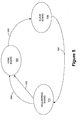
Referring now to Figure 5, a state diagram including the various communication paths
between a requesting board 510, a home board 520, and slave board 530 in servicing memory
access requests is illustrated, in accordance with one or more embodiments of the present
invention. The boards 510, 520, 530, in one embodiment, may include one or more boards
(e.g., expander board 40, system board 30, I/O board 35) of one or more control board sets
29(1-n). The term "memory access requests," as utilized herein may include, in one
embodiment, one or more of the processors 360(1-4) (see Figure 3) of a given system board
set 29(1-n) accessing one or more caches 362(1-4) or memories 361(1-4) in the system 10.
Although not so limited, for the purposes of this discussion, it is herein assumed that
one domain is configured in the system 10 that is formed of one or more complete (i.e., no
split expanders) system board sets 29(1-n). Generally, a given cache line in the system 10 is
associated with one home board 520. The requesting board 510 in the illustrated embodiment
represents a board attempting to access a selected cache line. The slave board 530 in the
illustrated embodiment represents a board that currently has a copy of a cache line that the
requesting board 510 is attempting to access. In a case where a current copy of a requested
cache line resides in the home board 520, then the home board 520 is also the slave board 530
for that transaction.
The requesting board 510 may initiate one of a variety of memory access transactions,
including request to own (RTO), request to share (RTS), WriteStream, WriteBack, and
ReadStream transactions. The one or more of the aforementioned memory access transactions
may be local or remote transactions, where local transactions may include transactions that are
broadcast locally within the system board set 29(1-n) and remote transactions may include
transactions that are directed to access cache lines from other system board sets 29(1-n).
Although not so limited, in one embodiment, an RTO request may be issued to obtain an
exclusive copy of a cache line, an RTS request to obtain a shared copy of a cache line, a
WriteBack transaction to write the cached line back to the home board, a ReadStream request
to get a snapshot copy of the cache line, and a WriteStream request to write a copy of the
cache line.
For illustrative purposes, an exemplary RTO transaction among the boards 510, 520,
and 530 is described below. For the purpose of this illustration, it is herein assumed that the
requesting board 510 is attempting to obtain write-access to a cache line owned by the home
board 520, where the latest copy of the requested cache line resides on the slave board 530.
The RTO request from the requesting board 510 is forwarded to the home board 520 via path
540. The forwarding of the RTO transaction from the requesting board 510 to the home board
520 is typically handled by the coherency module 382 (see Figure 3) of the requesting board
510 utilizing the address provided with the RTO request.
The requesting board 510 determines which of the home boards 520 has the requested
cache line by, for example, mapping the address of the cache line to the address ranges of the
caches associated with the various expander boards 40 within the system 10. When the home
board 520 receives the RTO message over the path 540, the coherency module 382 of the
home board 520 checks its directory cache 396 (see Figure 3) to determine if there is an entry
corresponding to the requested cache line. Assuming that an entry exists in the directory
cache 396, the home board 520 may reference the information stored in that entry to determine
that the slave board 530 currently has an exclusive copy of the requested cache line. It should
be noted, in one embodiment, that while the directory cache 396 of the home board 520 is
being referenced, the coherency module 382 may use the locking module 398 to at least
temporarily prevent other expander boards 40 from accessing that entry in the directory cache
396.
Based on the information stored in the directory cache 396, the home board 520 is able
to ascertain, in one embodiment, that the slave board 530 currently has an exclusive copy of
the cache line. Accordingly, the home board 520, in one embodiment, transmits a request over
a path 545 to the slave board 530 to forward a copy of the requested cache line to the
requesting board 510. In one embodiment, the slave board 530 downgrades its copy from an
exclusive copy (i.e., M-type) to an invalid copy (i.e., I-type) since, by definition, if one board
in the system 10 has an exclusive M-copy (i.e., the requesting board 510 in this case), all other
nodes should have invalid I-copies.
When the requesting board 510 receives a copy of the cache line over a path 550, it
internally notes that it now has an exclusive M-copy and acknowledges over a path 555.
When the home board 520 receives the acknowledgment message from the requesting board
510 over the path 555, the home board 520 updates its directory cache 396 to reflect that the
requesting board 510 now has the write-access to the cache line, and may use the locking
module 398 to allow other transactions involving the cache line to be serviced. The paths
540, 545, 550, and 555, in one embodiment, may be paths through the switch 20 (see Figures 1
and 3).
As other transactions occur for accessing cache lines in the home board 520, for
example, the coherency module 382 of the home board 520 routinely may update its directory
cache 396 to reflect the status of the referenced cache lines. The status of the referenced cache
lines may include information regarding the state of the cache line (e.g., M, I, S), ownership
rights, and the like. At any given time, because of the finite size of the directory cache 396, it
may be possible that a particular set 410 within the directory cache 396 may be full. When a
particular set 410 within the directory cache 396 is full, it may be desirable to discard or
overwrite old entries to store new entries. Because it may be desirable to retain some entries
in the directory cache 396 over others, a method, in accordance with one embodiment of the
present invention, for identifying entries that may be more desirable to retain than others is
illustrated in Figure 6.
In the method of Figure 6, the coherency module 382, in one embodiment, detects (at
605) a memory access transaction. As mentioned above, the memory access transaction may
include, but is not limited to, RTO, RTS, WriteStream, WriteBack, and ReadStream. The
coherency module 382, in one embodiment, determines (at 610) if an entry is to be stored (or
updated) in the directory cache 396. An entry may be stored in the directory cache 396, for
example, in response to a receipt of a memory access transaction (e.g., RTO, RTS) that may
have been initiated by the requesting board 510 (see Figure 5). However, in one embodiment,
not all of the memory access transactions may cause an entry to be created in the directory
cache 396. If it is determined (at 610) that no entry is to be stored in the directory cache 396,
then the method of Figure 6 continues (at 612) with its normal operation.
If, however, it is determined (at 610) that it is desirable to store an entry in the
directory cache 396, then the coherency module 382 determines (at 615) if the transaction
detected (at 605) is an RTO, WriteStream, or WriteBack transaction. If the transaction is one
of the three aforementioned transactions, then, in one embodiment, the coherency module 382
calculates (at 630) a retention value for the entry that is to be stored in the directory cache 396.
The retention value, in one embodiment, is indicative of whether it is desirable to victimize
one entry over another when the corresponding set 410 in the directory cache 396 is full, for
example. One way of calculating the retention value is shown in Figure 7, which is described
in more detail below. As explained earlier, the retention value of the entry stored in the
directory cache 396 may, for example, be saved in the retention bit field 475 (see Figure 4).
The coherency module 382, in one embodiment, stores (at 635) the entry and its
associated retention value in the directory cache 396. In one embodiment, a LRU value that is
associated with the entry stored (at 635) in the directory cache 396 is determined and stored (at
640). Subsequently, in one embodiment, the method of Figure 6 continues (at 612) with
normal operation.
If it is determined (at 615) that the memory access transaction is not at least one of an
RTO, WriteStream, and WriteBack transaction, then the coherency module 382, in one
embodiment, stores (at 645) the entry in the directory cache 396. Thus, although not so
limited, in the illustrated embodiment, a retention value is not calculated for an RTS
transaction, for example. The coherency module 382, in one embodiment, determines and
stores (at 640) an LRU value for the entry stored (at 645) and stores it in the directory cache
396. Subsequently, in one embodiment, the method of Figure 6 continues (at 612) with
normal operation.
Referring now to Figure 7, one embodiment of a method of calculating the retention
value of the block 630 of Figure 6 is illustrated, in accordance with the present invention. The
coherency module 382, in one embodiment, determines (at 710) whether the detected memory
access transaction (at 605 - see Figure 6) is either a WriteStream or WriteBack transaction
(i.e., as opposed to an RTO transaction). If the detected transaction is either a WriteStream or
WriteBack, then the coherency module 382 sets the retention value to zero.
Although not so limited, in the illustrated embodiment, a DC entry having a retention
value of zero is more likely to be victimized than a DC entry having a retention value of one.
A DC entry associated with a WriteStream or WriteBack transaction, in the illustrated
embodiment, is assigned a retention value of zero because such entries may be more
expendable relative to the other types of entries, as more fully explained below. Once the
retention value has been calculated, the method of Figure 7 continues to the step 635 of Figure
6, in one embodiment.
The coherency module 382, in one embodiment, determines (at 720) if the entry
desired to be stored (at 610 - see Figure 6) has a previously corresponding entry already stored
in the directory cache 396. If the directory cache 396 does not contain a previous
corresponding entry, then, in one embodiment, the coherency module 396 sets (at 715) the
retention value to zero. In this instance, since the entry that is desired to be stored (at 610 -
see Figure 6) is a new entry, it may be assigned a low retention priority relative to other entries
because the new entry may be more expendable as it may be less likely to be referenced again
once it is overwritten by another entry in the directory cache 396.
If it is determined (at 720) that a previous corresponding entry exists, then, in one
embodiment, the coherency module 382 determines (at 725) if the previously stored entry was
owned by the home board 520. If the previously stored entry is owned by the home board 520,
then the coherency module 382, in one embodiment, sets (at 715) the retention value to zero.
If it is determined (at 720) that a previous corresponding entry exists, then, in one
embodiment, the coherency module 382 determines (at 730) if the previously stored entry was
shared or owned by a board other than the home board 520. If yes, then the coherency module
382, in one embodiment, sets (at 740) the retention value to one. Although not so limited, in
the illustrated embodiment a previously stored entry that has a shared status (or "owned by
another board" status) is assigned a high retention value (i.e., one) because the cache line
associated with such an entry may be more likely to be accessed again in the near future. If
the previously stored entry was not shared or owned by a board other than the home board
520, then, in one embodiment, the retention bit value is set (at 715) to zero and the method of
Figure 7 thereafter may continue to the block 635 of Figure 6.
It should be appreciated that the method of Figure 7 provides one example of
calculating retention values, although, in other embodiments, a different scheme may be
employed, depending on the implementation. Furthermore, in alternative embodiments, the
priority given to selected memory access transactions may also vary from the described
embodiment.
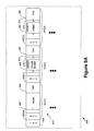
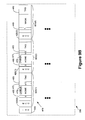
Referring now to Figures 8 and 9A-C, one embodiment of a method of victimizing one
or more entries in a particular set 410 of the directory cache 396 is illustrated. Figures 9A-C
illustrate a stylized embodiment of the directory cache 396 having a plurality of exemplary
entries 910(1-3), 920 (1-3) and 940 (1-3) stored within the set 410. In the description below,
reference to one or more of the Figures 9A-C are made whenever helpful in the understanding
of the illustrated embodiment of the method of Figure 8. For ease of illustration, a few
assumptions are made: in particular, it is herein assumed that the relevant set 410 of the
directory cache 396 of Figures 9A-C is full, the directory cache 396 is associated with the
home board 520 (see Figure 2), and the home board 520 has received a transaction for which it
is desirable to store a new entry in the filled set 410 of the directory cache 396.
In accordance with one embodiment of the present invention, and as is described in
more detail below, a stored entry in the set 410 of the directory cache 396 may be victimized
in the following order: (1) an invalid entry in the set 410 of the directory cache 396; (2) an
entry with a retention value of zero that is owned by the home board 520; (3) an entry with a
retention value of zero that has an owner other than the home board 520 or is a shared entry;
(4) an entry with a retention value of one. If more than one entry falls within one of the
above-described categories, then, in one embodiment, the LRM value in the LRM field 430
(see Figure 4) may be used to select at least one entry to victimize. It should be appreciated
that the above presented victimization order is exemplary in nature, and that, in other
embodiments, the order may vary, depending on the implementation.
In one embodiment, when accessing an entry in the directory cache 396, the coherency
module 382 may read the set 410 to which the entry belongs. Alternatively, in another
embodiment, the coherency module 382 may access the directory cache 396 on an entry-by-entry
basis. The manner in which the directory cache 396 is accessed may be implementation
specific.
Referring again to Figure 8, the coherency module 382 of the home board 520, in one
embodiment, determines (at 810) if the set 410 of the directory cache 396 contains one or more
entries 910(1-m) that are invalid. As mentioned earlier, in the illustrated embodiment, there
may be two types of entries stored in the directory cache 396: shared entries 910(1) or owned
entries 910(2-3). In one embodiment, the valid field 470 (see Figure 4) of the owned entries
437 (see Figure 4) may indicate which of the entries in the directory cache 396 are invalid.
The directory cache 396, after a reset or re-initialization, may initially contain invalidated
entries, for example. If the coherency module 382 of the home board 520 determines (at 810)
that one or more invalid entries are present in the directory cache 396, then the new entry may
be stored (at 815) in a slot occupied by one or more of the invalid entries.
For example, in Figure 9A, entry 910(2) of the directory cache 396 is an invalid entry,
as symbolically indicated by the letter "I" in the valid field 470. As such, in one embodiment,
the invalid entry 920(3) may be overwritten by the new entry. In the exemplary directory
cache 396 of the Figure 9A, the other owned entry 910(3) is a valid entry, as symbolically
represented by the letter "V" in the valid field 470 of the entry 910(3).
If there are no invalid entries in the set 410 of the directory cache 396, as is the case in
the exemplary directory cache 396 of Figure 9B, then the coherency module 382, in one
embodiment, determines (at 825) if any of the entries stored in the directory cache 396 have a
retention value of zero. For example, in the directory cache 396 of Figure 9B, the entries
920(1-2) have a retention value of zero, as indicated by the "0" stored in the retention field
465. As explained above, in the illustrated embodiment, entries having a retention value of
zero may be more expendable as compared to those with a retention value in a given set 410.
If there are one or more entries with a retention value of zero, then the coherency
module 382, in one embodiment, determines (at 830) if the owner of such an entry(or entries)
is the home board 520. If the owner is the home board 520, then the coherency module 582
may determine (at 835) whether there is more than one entry with a retention value of zero for
which the owner is the home board 520. In Figure 9B, among the entries 920(1-2) with a
retention value of zero, both of the entries 920(1-2) have the home board 520 as the owner.
If the coherency module 382 determines (at 835) that there are more than one entries
with a retention value of zero for which the owner is the home board 520, as is the case in the
directory cache 396 of Figure 9B, then the coherency module 382, in one embodiment,
identifies (at 840) one of those entries based on the LRM value associated with the entries and
overwrites that entry with the new entry. For example, in Figure 9B, entries 920(1-2) each has
a retention value of zero and the home board 520 as the owner. To determine which of the two
entries 920(1-2) to replace with the new entry, the LRM bits ("100") in the LRM field 430 are
used to determine which of the two entries 920(1-2) was least recently modified. As shown in
Table 2 above, the sequence of LRM bits "100" indicates, in the illustrated embodiment, that
the most recently modified field is 920(1), and the least recently modified field is 920(2). As
such, the field 920(2) in the illustrated example of Figure 9B would be victimized to make
room for the new entry.
If (at 835) there is not more than one entry (i.e., there is only one entry with R=0 and
Home=Home Board), then the coherency module 382, in one embodiment, replaces (at 837)
that one entry that has a retention value of zero and has the home board 520 as the owner with
the new entry.
If it is determined (at 830) that the owner of the entry (or entries) having a retention
value of zero is not the home board 520, then, in one embodiment, the coherency module 382
determines (at 845) if there are one or more entries with retention value of zero for which the
owner is not the home board 520 (i.e., some board other than the home board 520 is the owner
of that entry). If it is determined (at 845) there is only entry with the retention value equal to
zero and that has an owner that is not the home board 520, then that entry is overwritten (at
837) by the new entry.
If the coherency module 382 determines (at 845) that there are more than one entries
with a retention value of zero for which the owner is not the home board 520, then the
coherency module 382, in one embodiment, identifies (at 840) one of those entries based on
the LRM value associated with the entries and overwrites that entry with the new entry.
The coherency module 382, in one embodiment, determines (at 855) whether any of
the stored entries in the directory cache 396 have a shared status (i.e., as opposed to an
"owned" status). For example, with reference to Figure 9B, the entry 920(3) is a shared entry,
as indicated by a "1" in the identifier field 440. The "shared status," as mentioned earlier,
indicates that the entry is being shared by one or more boards 40 in the board sets 29(1-n) in
the system 10. If it is determined (at 855) that there is at least one entry with the shared status,
then the coherency module 382, in one embodiment, determines (at 860) if the directory cache
396 includes more than one shared entry. If only one shared entry exists, then the coherency
module 382 overwrites (at 865) that shared entry with the new entry. In the illustrated
example of Figure 9B, there is only one shared entry 920(1). As such, in the illustrated
example, the shared entry 920(3) may be overwritten by the new entry. If, however, more than
one shared entry exists in the directory cache 396, then the coherency module 382, in one
embodiment, identifies (at 840) one entry out of those entries based on an associated LRM
value and then overwrites the identified entry with the new entry.
The coherency module 382, in one embodiment, determines (at 870) if more than one
entry exists with a retention value of one. If there is not more than one entry in the directory
cache with a retention value of one (i.e., there is only one such entry), then the coherency
module 382 may overwrite (at 865) that entry with the new entry. If, however, it is determined
(at 870) that there is more than one entry with the retention value equal to one, then, the
coherency module 382, in one embodiment, identifies (at 840) one entry out of those entries
based on the LRM value associated with the stored entries and overwrites the identified entry
with the new entry.
For example, as shown in Figure 9C, the entries 940(1-3) have a retention value of one,
as indicated by numeral "1" stored in the retention bit field 475 of each entry 940(1-3). Since
there is more than one entry with a retention value of one, in the illustrated example, the LRM
bits ("010") in the LRM field 430 are utilized to select one of the three entries 940(1-3) to
victimize. In the illustrated embodiment, LRM bits "010" indicate that entry 940(2) is the
least recently modified (see Table 2), and, as such, entry 940(2) is overwritten by the new
entry.
The various system layers, routines, or modules may be executable control units (such
as control unit 389 (see Figure 3). Each control unit may include a microprocessor, a
microcontroller, a digital signal processor, a processor card (including one or more
microprocessors or controllers), or other control or computing devices.
The storage devices referred to in this discussion may include one or more machine-readable
storage media for storing data and instructions. The storage media may include
different forms of memory including semiconductor memory devices such as dynamic or static
random access memories (DRAMs or SRAMs), erasable and programmable read-only
memories (EPROMs), electrically erasable and programmable read-only memories
(EEPROMs) and flash memories; magnetic disks such as fixed, floppy, removable disks; other
magnetic media including tape; and optical media such as compact disks (CDs) or digital
video disks (DVDs). Instructions that make up the various software layers, routines, or
modules in the various systems may be stored in respective storage devices. The instructions
when executed by a respective control unit cause the corresponding system to perform
programmed acts.
The instructions can be provided as one or more computer programs, routines,
modules, software layers, etc. on one or more carrier media. Suitable carrier media include a
storage medium such as, by way of example only, optical, magneto optical, magnetic, solid
state, tape or disk storage media, or a transmission medium such as, by way of example only,
wired, wireless, optical or electromagnetic media forming part, for example, of a network,
point to point, or broadcast communications medium.
An aspect of the invention can provide a method, comprising: detecting a memory
access transaction; determining a retention value based on the type of memory access
transaction; and storing the retention value in an entry associated with the memory access
transaction.
Another aspect of the invention can provide an article comprising one or more
machine-readable storage media containing instructions that when executed enable a processor
to: perform coherence for memory transactions within a first system board set using a first
coherence scheme; and perform coherence for memory transactions between the first system
board set and a second system board set using a second coherence scheme, wherein the second
coherence scheme employs a retention value associated with one or more entries stored in a
directory cache to identify which entry to victimize when storing a new entry.
A further aspect of the invention can provide a directory cache, comprising: an address
field to store an address associated with an entry; a modified state field to indicate an order in
which the entry was modified relative to at least one other entry; and a retention field to store a
retention value associated with the entry, wherein the retention value indicates whether it is
desirable to retain the entry in the directory cache.
Another aspect of the invention can provide an apparatus, comprising: a directory
cache; and a control unit adapted to detect a memory access transaction, determine a retention
value based on the type of memory access transaction, and store the retention value associated
with the memory access transaction in the directory cache.
The particular embodiments disclosed above are illustrative only, as the invention may
be modified and practiced in different but equivalent manners apparent to those skilled in the
art having the benefit of the teachings herein. Furthermore, no limitations are intended to the
details of construction or design herein shown, other than as described in the claims below. It
is therefore evident that the particular embodiments disclosed above may be altered or
modified and all such variations are considered within the scope of the invention.