EP1304613A2 - Random number generating system and its method - Google Patents
Random number generating system and its method Download PDFInfo
- Publication number
- EP1304613A2 EP1304613A2 EP02023010A EP02023010A EP1304613A2 EP 1304613 A2 EP1304613 A2 EP 1304613A2 EP 02023010 A EP02023010 A EP 02023010A EP 02023010 A EP02023010 A EP 02023010A EP 1304613 A2 EP1304613 A2 EP 1304613A2
- Authority
- EP
- European Patent Office
- Prior art keywords
- random number
- data
- shift register
- number generator
- card
- Prior art date
- Legal status (The legal status is an assumption and is not a legal conclusion. Google has not performed a legal analysis and makes no representation as to the accuracy of the status listed.)
- Withdrawn
Links
Images



Classifications
-
- G—PHYSICS
- G06—COMPUTING OR CALCULATING; COUNTING
- G06F—ELECTRIC DIGITAL DATA PROCESSING
- G06F7/00—Methods or arrangements for processing data by operating upon the order or content of the data handled
- G06F7/58—Random or pseudo-random number generators
- G06F7/588—Random number generators, i.e. based on natural stochastic processes
Definitions
- the present invention relates to a random number generating system and its method.
- a conventional random number generating system there is shown a conventional random number generating system.
- a random number generating system using a linear feedback shift register hereinafter, referred to as LFSR.
- the conventional random number generator using the LFSR comprises an n-stage shift register (S i-1 , S i-2 , ---, S i-n ) 501, tap strings (C 1 , C 2 , ---, C n ) 502, and an exclusive OR (XOR) circuit group 503.
- the shift register 501 shifts preset initial value data by a single bit to the left in synchronization with a clock signal CLK.
- the tap strings 502 C 1 to C n are preset to 0 or 1.
- the conventional random number generator generates random numbers conforming to the following procedure. Note that, however, procedure (2) and procedure (3) are progressed simultaneously.
- a period of a generated random number depends upon the number of stages n of the shift register 501 and a preset value of the tap string 502.
- the conventional random number generator generates an identical random number at the same timing if an identical initial value is set, and therefore it is hard to obtain irregular random numbers in this constitution.
- a random number generating system typically, it has a random number generator for generating random numbers, wherein the random number generator generates random numbers by using data transmitted to a functional block arranged outside the random number generator.
- a semiconductor integrated circuit mounted on an IC card is described by using Fig. 1.
- Fig. 1 there is shown a block diagram of a general semiconductor integrated circuit mounted on an IC card.
- the IC card comprises a contact section 101 for exchanging data or the like with an IC card read-writer, a control section 102 for controlling the entire semiconductor integrated circuit mounted on the IC card, a read only memory (hereinafter, referred to as ROM) 103 for storing a control program or the like executed by the control section 102, a writable and readable memory (hereinafter, referred to as RAM) 104 used when the control section 102 executes the control program, an electrically erasable ROM (hereinafter, referred to as EEPROM) 105 for storing mainly variable data such as transaction data, a random number generator 106 for generating random numbers, and a data bus 107.
- EEPROM electrically erasable ROM
- the contact section 101 comprises a supply voltage terminal VDD and a ground voltage terminal GND to which a supply voltage and a ground voltage are supplied from a supply circuit (not shown) of the IC card read-writer, a clock terminal CLK to which a clock signal is supplied from a clock circuit (not shown) of the IC card read-writer, a reset terminal RES to which a reset signal is supplied from a reset circuit (not shown) of the IC card read-writer, and a data input-output terminal SIO where serial data is inputted from a data input-output circuit (not shown) of the IC card read-writer and where data from the control section 102 of the IC card is outputted as serial data to an input-output circuit of the IC card read-writer.
- the control section 102 is a CPU, where a supply voltage, a ground voltage, a clock signal, a reset signal, and data are inputted from the contact section 101 and then data is outputted to the data input-output terminal SIO of the contact section 101.
- the random number generator 106 is connected to the control section 102 and the memories (ROM 103, the RAM 104, and the EEPROM 105) via the data bus 107. Random numbers generated by the random number generator 106 are used for a password decryption or in a scramble transmission in the data bus 107.
- serial data is exchanged via the data input-output terminal (hereinafter, referred to as SIO terminal) of the IC card and the data input-output circuit of the IC card read-writer.
- This data is transaction information or the like, which is data transmitted for processing to the outside of the random number generator, for example, to the CPU.
- Data is exchanged between the IC card and the external equipment IC card read-writer in start-stop synchronization and therefore the serial data changes at asynchronous timing.
- random numbers are generated on the basis of the serial data.
- the random number generating system comprises a signal line 201 and a random number generator 202 for generating random numbers by using data of the signal line 201.
- the signal line 201 is connected to functional blocks.
- the functional blocks include the CPU, the memories (the ROM, the RAM, and the EEPROM), and the like. These CPU and the memories are not arranged anew for the random number generating system according to the present invention, but those generally mounted on an IC card.
- Data transmitted through the signal line 201 is serial data transmitted or received between the IC card and the IC card read-writer.
- the random number generator 202 is provided with a linear feedback shift register (LFSR).
- This random number generator 202 comprises a first shift register 203 and a second shift register 204 for shifting preset initial value data by a single bit to the left in synchronization with a clock signal CLK, a logic device (XOR circuit) 205 for executing a logical operation (exclusive OR) between data transmitted through the signal line 201, namely, serial data transmitted or received with the IC card read-writer via the SIO terminal of the IC card and an output of the first shift register 203 and then inputting a result of the operation to the second shift register 204, and a logic device (XOR circuit) 206 for executing a logical operation between an output of a register Bit2 of the first shift register 203 and an output of the second shift register 204 and then feeding back a result of the operation S i for the input to the first shift register 203.
- a logic device (XOR circuit) 206 for executing a logical operation between an output of a
- first shift register 203 is a 3-bit register formed by register Bit1 to register Bit3 and the second shift register 204 is a 5-bit register formed by register Bit4 to register Bit8 in this embodiment, they are not limited thereto.
- result S i of the logical operation exclusive OR
- the operation is not limited thereto, but it is also possible to execute a logical operation of outputs from arbitrary and a plurality of registers among the register Bit1 to Bit8 and then to feed back a result of the operation for the input to the first shift register 203.
- the random number generating system according to the present invention generates random numbers conforming to the following procedure. Note that, however, Procedure (2) to Procedure (4) are progressed simultaneously.
- Procedure (1) a random number generated at a use of the previous IC card and then stored in a memory is used as the initial value used for the settings of the first shift register 203 and the second shift register 204.
- Procedure (1) it is also possible to use data stored in a data storage section of the CPU arranged in the periphery of the random number generator 202 as means for setting the first shift register 203 and the second shift register 204 to the initial value.
- the randomnumber generating system executes a logical operation between data transmitted for use to the functional block (the CPU or the memories) arranged outside the random number generator such as, for example, serial data transmitted or received between the IC card and the IC card read-writer and an output of the first shift register 203 and then inputs a result of the operation to the second shift register 204, thereby enabling a generation of very irregular random numbers, and no circuit is arranged anew outside the random number generator 202, thereby preventing an increase of a consumed current and an expansion of a chip in size.
- the functional block the CPU or the memories
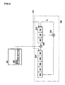
- Fig. 3 there is shown a circuit diagram illustrating a constitution of the random number generating system according to the second embodiment of the present invention.
- the random number generating system according to this embodiment differs from the random number generating system according to the first embodiment shown in Fig. 2 in that the signal line 201 in Fig. 2 is replaced with a signal line (data bus) 301.
- Other circuit components are the same as those of the random number generating system according to the first embodiment shown in Fig. 3 and therefore the same reference numerals are appended to those in the following description.
- a data bus 301 is not arranged anew according to the present invention, but conventionally arranged between functional blocks mounted on an IC card.
- the functional blocks include the CPU and the memories, the ROM, RAM, and EEPROM or the like.
- Data transmitted through the data bus 301 for connecting these functional blocks with each other varies whenever the CPU accesses the ROM, RAM, or EEPROM.
- data transmitted through the data bus is transmitted in synchronization with a clock signal, a data pattern on the data bus varies irregularly due to different access times of the memories (the ROM, RAM, EEPROM, etc.). It results in an increase of irregularity of data inputted from the data bus 301 to the logic device (XOR circuit) 205, thereby increasing irregularity of data inputted from the logic device (XOR circuit) 205 to the second shift register 204.
- Data written into memories (the ROM, RAM, and EEPROM, etc.) in the random number generating system mounted on the IC card or data read from these memories depends upon an IC card and further varies whenever the IC card is used. It results in an increase of irregularity of data inputted from the data bus 301 to the logic device 205, thereby increasing irregularity of a data value inputted from the logic device 205 to the second shift register 204.
- Procedure (3) The logic device (XOR circuit) 205 executes a logical operation (exclusive OR) between an output from the first shift register 203 and a data value transmitted through the signal line (data bus) and then inputs a result of the operation to the second shift register 204.
- a logical operation exclusive OR
- the random number generating system executes a logical operation between a data value transmitted through a data bus connecting a plurality of the functional blocks (the CPU, memories, etc.) with each other and an output from the first shift register 203 and then inputs a result of the operation to the second shift register 204, thereby generating very irregular random numbers, and no circuit is arranged anew outside the random number generator 202, thereby preventing an increase of a consumed current and an expansion of a chip in size.
- FIG. 4 there is shown a circuit diagram illustrating a random number generating system according to the third embodiment of the present invention.
- the random number generating system according to this embodiment differs from the random number generating system according to the first embodiment shown in Fig. 2 in that data inputted from the signal line 201 in Fig. 2 to the logic device (XOR circuit) 205 is replaced with data stored in a data storage section 402 of a CPU 401.
- the CPU 401 is not arranged anew according to the present invention, but generally mounted on an IC card.
- Other circuit components are the same as those of the random number generating system according to the first embodiment shown in Fig. 2, and therefore the same reference numerals are appended to those in the following description.
- the data storage section 402 is an accumulator in the CPU 401 or a general-purpose register used for an operation very frequently in case of a CPU having no accumulator.
- This accumulator or general-purpose register is not arranged anew according to the present invention, but conventionally arranged in a CPU.
- Data inputted from the accumulator (or the general-purpose register) 402 to the logic device (XOR circuit) 205 varies whenever a program is processed in the CPU 401.
- this data changes when a program processing flow is different or when data used for an operation of the CPU, namely, data inputted from external equipment or data read from a memory is different.
- data stored in the accumulator (or the general-purpose register) 402 forming the CPU varies according to data supplied from the IC card read-writer which is external equipment or data read from the memory mounted on the IC card. It results in an increase of irregularity of a data value inputted from the accumulator (or the general-purpose register) 402 to the logic device 205, thereby increasing irregularity of a data value inputted from the logic device 205 to the second shift register 204.
- Procedure (3) The logic device 205 executes a logical operation (exclusive OR) between an output from the first shift register 203 and data stored in the accumulator (or the general-purpose register) 402 of the CPU 401 and then inputs a result of the operation to the second shift register 204.
- a logical operation exclusive OR
- the random number generating system executes a logical operation between data stored in the data storage section (the accumulator or the general-purpose register) 402 forming the CPU 401 and an output from the first shift register 203 and then inputs a result of the operation to the second shift register 204, thereby generating very irregular random numbers, and no circuit is arranged anew outside the random number generator 202, thereby preventing an increase of a consumed current and an expansion of a chip in size.
- the random number generating system according to this embodiment differs from the random number generating system according to the third embodiment in that the accumulator (or the general-purpose register) 401 in the third embodiment is replaced with a PSW (program status word).
- This PSW is not arranged anew according to the present invention, but conventionally arranged in a CPU.
- Other circuit components are the same as those of the random number generating system according to the third embodiment shown in Fig. 4. Accordingly, this embodiment will be described by referring to Fig. 4.
- the PSW 402 is arranged in a control circuit in the CPU.
- This control circuit controls a memory unit (not shown) and an operation unit (not shown) arranged in the CPU according to a result of decoding of an instruction decoding unit (not shown) arranged in the PSW 402 or the CPU.
- Data stored in the PSW 402 is a control flag such as, for example, an operation carry or a zero (0) flag. This control flag varies in a complex manner and irregularly according to program processing and operational processing in the CPU 401.
- the control flag allocated to this PSW 402 such as, for example, an operation carry, a zero (o) flag, or a result of a logical operation of these plural values is inputted to the logic device 205 for use.
- the logic device 205 executes a logical operation (exclusive OR) between data stored in the PSW 402 and an output from the first shift register 203 and then inputs a result of the operation to the second shift register 204.
- Data stored in the PSW varies according to a difference of a program processing flow or to a difference of data used for operational processing by the CPU, namely, data inputted from external equipment or data read from a memory.
- Data stored in the PSW 402 arranged in the CPU in the random number generating system mounted on the IC card varies according to data supplied from the IC card read-writer which is external equipment or to data read from the memory mounted on the IC card. It results in an increase of irregularity of a data value inputted from the PSW 402 to the logic device (XOR circuit) 205, thereby increasing irregularity of a data value inputted from the logic device 205 to the second shift register 204.
- Procedure (3) The logic device 205 executes a logical operation (exclusive OR) between an output from the first shift register 203 and a data value stored in the PSW (program status word) 402 arranged in the CPU and then inputs a result of the operation to the second shift register 204.
- a logical operation exclusive OR
- the random number generating system executes a logical operation between data stored in the data storage section (PSW: program status word) 402 arranged in the CPU and an output from the first shift register 203 and then inputs a result of the operation to the second shift register 204, thereby generating very irregular random numbers, and no circuit is arranged anew outside the random number generator 202, thereby preventing an increase of a consumed current and an expansion of a chip in size.
- PSW program status word
- the system according to the present invention typically has a random number generator for generating random numbers, wherein the random number generator generates random numbers by using data transmitted to a functional block arranged outside the random number generator, thereby enabling a generation of very irregular random numbers without any increase of a consumed current nor expansion of a chip in size.
Landscapes
- Physics & Mathematics (AREA)
- General Physics & Mathematics (AREA)
- Engineering & Computer Science (AREA)
- Theoretical Computer Science (AREA)
- Computational Mathematics (AREA)
- Mathematical Analysis (AREA)
- Mathematical Optimization (AREA)
- Pure & Applied Mathematics (AREA)
- General Engineering & Computer Science (AREA)
- Tests Of Electronic Circuits (AREA)
- Semiconductor Integrated Circuits (AREA)
- Storage Device Security (AREA)
Abstract
Description
Procedure (3) : The logic device (XOR circuit) 205 executes a logical operation (exclusive OR) between an output from the first shift register 203 and a data value transmitted through the signal line (data bus) and then inputs a result of the operation to the second shift register 204.
Procedure (3) : The logic device 205 executes a logical operation (exclusive OR) between an output from the first shift register 203 and data stored in the accumulator (or the general-purpose register) 402 of the CPU 401 and then inputs a result of the operation to the second shift register 204.
Procedure (3) : The logic device 205 executes a logical operation (exclusive OR) between an output from the first shift register 203 and a data value stored in the PSW (program status word) 402 arranged in the CPU and then inputs a result of the operation to the second shift register 204.
Claims (21)
Applications Claiming Priority (2)
| Application Number | Priority Date | Filing Date | Title |
|---|---|---|---|
| JP2001319460A JP2003122560A (en) | 2001-10-17 | 2001-10-17 | Random number generation system and random number generation method |
| JP2001319460 | 2001-10-17 |
Publications (2)
| Publication Number | Publication Date |
|---|---|
| EP1304613A2 true EP1304613A2 (en) | 2003-04-23 |
| EP1304613A3 EP1304613A3 (en) | 2005-06-08 |
Family
ID=19137010
Family Applications (1)
| Application Number | Title | Priority Date | Filing Date |
|---|---|---|---|
| EP02023010A Withdrawn EP1304613A3 (en) | 2001-10-17 | 2002-10-15 | Random number generating system and its method |
Country Status (3)
| Country | Link |
|---|---|
| US (1) | US20030074380A1 (en) |
| EP (1) | EP1304613A3 (en) |
| JP (1) | JP2003122560A (en) |
Cited By (1)
| Publication number | Priority date | Publication date | Assignee | Title |
|---|---|---|---|---|
| FR2896057A1 (en) * | 2006-01-12 | 2007-07-13 | St Microelectronics Sa | Random number generating method for e.g. communication interface, involves generating oscillator signals at same median frequency and having distinct phase, and sampling state of each signal at appearance of binary signal |
Families Citing this family (2)
| Publication number | Priority date | Publication date | Assignee | Title |
|---|---|---|---|---|
| JP5231079B2 (en) | 2008-04-25 | 2013-07-10 | ルネサスエレクトロニクス株式会社 | Pseudorandom number generator and data communication device |
| CN115079999A (en) * | 2022-06-22 | 2022-09-20 | 长鑫存储技术有限公司 | Random data generation circuit and read-write training circuit |
Family Cites Families (7)
| Publication number | Priority date | Publication date | Assignee | Title |
|---|---|---|---|---|
| US4785410A (en) * | 1985-06-05 | 1988-11-15 | Clarion Co., Ltd. | Maximum length shift register sequences generator |
| EP0582083A1 (en) * | 1992-08-05 | 1994-02-09 | Motorola, Inc. | A method and apparatus for generating pseudo-random numbers |
| US5867409A (en) * | 1995-03-09 | 1999-02-02 | Kabushiki Kaisha Toshiba | Linear feedback shift register |
| JP2000222176A (en) * | 1999-02-03 | 2000-08-11 | Mitsubishi Electric Corp | Random number generation circuit, non-contact IC card and reader / writer incorporating the random number generation circuit, and test method for device incorporating the random number generation circuit |
| US6678707B1 (en) * | 2000-10-30 | 2004-01-13 | Hewlett-Packard Development Company, L.P. | Generation of cryptographically strong random numbers using MISRs |
| US6807553B2 (en) * | 2001-04-23 | 2004-10-19 | Safenet B.V. | Digital true random number generator circuit |
| US20020186086A1 (en) * | 2001-06-12 | 2002-12-12 | Dallas Semiconductor Corporation | Random number generator |
-
2001
- 2001-10-17 JP JP2001319460A patent/JP2003122560A/en active Pending
-
2002
- 2002-10-15 EP EP02023010A patent/EP1304613A3/en not_active Withdrawn
- 2002-10-17 US US10/271,562 patent/US20030074380A1/en not_active Abandoned
Cited By (3)
| Publication number | Priority date | Publication date | Assignee | Title |
|---|---|---|---|---|
| FR2896057A1 (en) * | 2006-01-12 | 2007-07-13 | St Microelectronics Sa | Random number generating method for e.g. communication interface, involves generating oscillator signals at same median frequency and having distinct phase, and sampling state of each signal at appearance of binary signal |
| EP1816560A1 (en) * | 2006-01-12 | 2007-08-08 | Stmicroelectronics Sa | Method and device for generating a random number in a USB peripheral device |
| US7958175B2 (en) | 2006-01-12 | 2011-06-07 | Stmicroelectronics Sa | Method and device for generating a random number in a USB (universal serial bus) peripheral |
Also Published As
| Publication number | Publication date |
|---|---|
| EP1304613A3 (en) | 2005-06-08 |
| US20030074380A1 (en) | 2003-04-17 |
| JP2003122560A (en) | 2003-04-25 |
Similar Documents
| Publication | Publication Date | Title |
|---|---|---|
| US7036017B2 (en) | Microprocessor configuration with encryption | |
| EP3709157B1 (en) | Random number generator | |
| US7376687B2 (en) | Pseudo-random number generator | |
| EP1073021B1 (en) | Information processing apparatus, card and information processing system | |
| EP0342832A2 (en) | Dynamic feedback arrangement scrambling technique keystream generator | |
| US20080025506A1 (en) | Memory access control apparatus and method, and communication apparatus | |
| US20120243636A1 (en) | Semiconductor device and memory system | |
| KR20040087910A (en) | Scrambler circuit, descrambler circuit, data processing device and ic card | |
| US7319758B2 (en) | Electronic device with encryption/decryption cells | |
| CN101366231A (en) | Cryptographic operation processing circuit | |
| JP5231079B2 (en) | Pseudorandom number generator and data communication device | |
| US20030074380A1 (en) | Random number generating system and its method | |
| US5828826A (en) | Processing apparatus having a nonvolatile memory to which a supply voltage is supplied through a shared terminal | |
| US8275972B2 (en) | Write data mask method and system | |
| CN102237867A (en) | Semiconductor module including module control circuit and method for controlling the same | |
| US6972609B2 (en) | Semiconductor integrated circuit device with a plurality of internal circuits operable in synchronism with internal clock | |
| US11928077B2 (en) | Data processing circuit, data storage device including the same, and operating method thereof | |
| US6505304B1 (en) | Timer apparatus which can simultaneously control a plurality of timers | |
| US7949698B2 (en) | Circuit arrangement and method for initializing a random number generator | |
| JP2006318475A (en) | Random number distribution generation system and method in a device with limited processing and storage capabilities | |
| KR100968417B1 (en) | Semiconductor memory device | |
| US7502814B2 (en) | Device and method for generating a pseudorandom sequence of numbers | |
| JP3910589B2 (en) | A data processing device that changes keys at irregular time intervals | |
| JP2007281994A (en) | Semiconductor integrated circuit | |
| JP4743783B2 (en) | Memory system |
Legal Events
| Date | Code | Title | Description |
|---|---|---|---|
| PUAI | Public reference made under article 153(3) epc to a published international application that has entered the european phase |
Free format text: ORIGINAL CODE: 0009012 |
|
| AK | Designated contracting states |
Designated state(s): AT BE BG CH CY CZ DE DK EE ES FI FR GB GR IE IT LI LU MC NL PT SE SK TR |
|
| AX | Request for extension of the european patent |
Extension state: AL LT LV MK RO SI |
|
| PUAL | Search report despatched |
Free format text: ORIGINAL CODE: 0009013 |
|
| AK | Designated contracting states |
Kind code of ref document: A3 Designated state(s): AT BE BG CH CY CZ DE DK EE ES FI FR GB GR IE IT LI LU MC NL PT SE SK TR |
|
| AX | Request for extension of the european patent |
Extension state: AL LT LV MK RO SI |
|
| 17P | Request for examination filed |
Effective date: 20051121 |
|
| AKX | Designation fees paid |
Designated state(s): DE FR GB |
|
| STAA | Information on the status of an ep patent application or granted ep patent |
Free format text: STATUS: THE APPLICATION HAS BEEN WITHDRAWN |
|
| 18W | Application withdrawn |
Effective date: 20061108 |