EP1304585A1 - Optical element having wavelength selectivity - Google Patents
Optical element having wavelength selectivity Download PDFInfo
- Publication number
- EP1304585A1 EP1304585A1 EP01949938A EP01949938A EP1304585A1 EP 1304585 A1 EP1304585 A1 EP 1304585A1 EP 01949938 A EP01949938 A EP 01949938A EP 01949938 A EP01949938 A EP 01949938A EP 1304585 A1 EP1304585 A1 EP 1304585A1
- Authority
- EP
- European Patent Office
- Prior art keywords
- lens array
- optical element
- face
- layered film
- film filter
- Prior art date
- Legal status (The legal status is an assumption and is not a legal conclusion. Google has not performed a legal analysis and makes no representation as to the accuracy of the status listed.)
- Withdrawn
Links
- 230000003287 optical effect Effects 0.000 title claims abstract description 129
- 238000004519 manufacturing process Methods 0.000 claims abstract description 17
- 239000000758 substrate Substances 0.000 claims description 10
- 238000000034 method Methods 0.000 claims description 6
- 230000008020 evaporation Effects 0.000 claims description 5
- 238000001704 evaporation Methods 0.000 claims description 5
- 238000005240 physical vapour deposition Methods 0.000 claims description 5
- 239000010408 film Substances 0.000 description 67
- 238000004544 sputter deposition Methods 0.000 description 5
- 238000000151 deposition Methods 0.000 description 3
- 230000008021 deposition Effects 0.000 description 3
- 238000010030 laminating Methods 0.000 description 2
- 239000013307 optical fiber Substances 0.000 description 2
- 239000010409 thin film Substances 0.000 description 2
- VYPSYNLAJGMNEJ-UHFFFAOYSA-N Silicium dioxide Chemical compound O=[Si]=O VYPSYNLAJGMNEJ-UHFFFAOYSA-N 0.000 description 1
- 238000003491 array Methods 0.000 description 1
- 238000010420 art technique Methods 0.000 description 1
- 230000002238 attenuated effect Effects 0.000 description 1
- 238000010586 diagram Methods 0.000 description 1
- 230000010354 integration Effects 0.000 description 1
- 238000001659 ion-beam spectroscopy Methods 0.000 description 1
- 150000002500 ions Chemical class 0.000 description 1
- 238000001755 magnetron sputter deposition Methods 0.000 description 1
- BPUBBGLMJRNUCC-UHFFFAOYSA-N oxygen(2-);tantalum(5+) Chemical compound [O-2].[O-2].[O-2].[O-2].[O-2].[Ta+5].[Ta+5] BPUBBGLMJRNUCC-UHFFFAOYSA-N 0.000 description 1
- 239000011347 resin Substances 0.000 description 1
- 229920005989 resin Polymers 0.000 description 1
- 229910052814 silicon oxide Inorganic materials 0.000 description 1
- 229910001936 tantalum oxide Inorganic materials 0.000 description 1
- 238000002834 transmittance Methods 0.000 description 1
- 238000001771 vacuum deposition Methods 0.000 description 1
- 238000007740 vapor deposition Methods 0.000 description 1
Images


Classifications
-
- G—PHYSICS
- G02—OPTICS
- G02B—OPTICAL ELEMENTS, SYSTEMS OR APPARATUS
- G02B5/00—Optical elements other than lenses
- G02B5/20—Filters
- G02B5/28—Interference filters
- G02B5/285—Interference filters comprising deposited thin solid films
-
- G—PHYSICS
- G02—OPTICS
- G02B—OPTICAL ELEMENTS, SYSTEMS OR APPARATUS
- G02B5/00—Optical elements other than lenses
- G02B5/20—Filters
- G02B5/201—Filters in the form of arrays
-
- G—PHYSICS
- G02—OPTICS
- G02B—OPTICAL ELEMENTS, SYSTEMS OR APPARATUS
- G02B6/00—Light guides; Structural details of arrangements comprising light guides and other optical elements, e.g. couplings
- G02B6/24—Coupling light guides
- G02B6/26—Optical coupling means
- G02B6/28—Optical coupling means having data bus means, i.e. plural waveguides interconnected and providing an inherently bidirectional system by mixing and splitting signals
- G02B6/293—Optical coupling means having data bus means, i.e. plural waveguides interconnected and providing an inherently bidirectional system by mixing and splitting signals with wavelength selective means
- G02B6/29346—Optical coupling means having data bus means, i.e. plural waveguides interconnected and providing an inherently bidirectional system by mixing and splitting signals with wavelength selective means operating by wave or beam interference
- G02B6/29361—Interference filters, e.g. multilayer coatings, thin film filters, dichroic splitters or mirrors based on multilayers, WDM filters
-
- G—PHYSICS
- G02—OPTICS
- G02B—OPTICAL ELEMENTS, SYSTEMS OR APPARATUS
- G02B6/00—Light guides; Structural details of arrangements comprising light guides and other optical elements, e.g. couplings
- G02B6/24—Coupling light guides
- G02B6/26—Optical coupling means
- G02B6/28—Optical coupling means having data bus means, i.e. plural waveguides interconnected and providing an inherently bidirectional system by mixing and splitting signals
- G02B6/293—Optical coupling means having data bus means, i.e. plural waveguides interconnected and providing an inherently bidirectional system by mixing and splitting signals with wavelength selective means
- G02B6/29379—Optical coupling means having data bus means, i.e. plural waveguides interconnected and providing an inherently bidirectional system by mixing and splitting signals with wavelength selective means characterised by the function or use of the complete device
- G02B6/2938—Optical coupling means having data bus means, i.e. plural waveguides interconnected and providing an inherently bidirectional system by mixing and splitting signals with wavelength selective means characterised by the function or use of the complete device for multiplexing or demultiplexing, i.e. combining or separating wavelengths, e.g. 1xN, NxM
-
- G—PHYSICS
- G02—OPTICS
- G02B—OPTICAL ELEMENTS, SYSTEMS OR APPARATUS
- G02B6/00—Light guides; Structural details of arrangements comprising light guides and other optical elements, e.g. couplings
- G02B6/24—Coupling light guides
- G02B6/26—Optical coupling means
- G02B6/32—Optical coupling means having lens focusing means positioned between opposed fibre ends
Definitions
- the present invention relates to an optical element having wavelength selectivity, and, more particularly, to an optical element which multiplexes lights of different wavelengths or demultiplexes multiplexed light wavelength by wavelength.
- Optical elements using an optical fiber and collimator lens have conventionally been used as optical communication equipment parts.
- optical communication becomes very popular from now on, miniaturization and integration of optical communication equipment parts become further essential.
- Optical communication requires a technique which demultiplexes light by selectively transmitting or reflecting light wavelength by wavelength.
- a multi-layered film filter which has high refractive-index dielectric layers and low refractive-index dielectric layers alternately laminated, e.g., an edge filter or a narrow-band filter, is known as an optical filter.
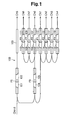
- An optical communication equipment part 100 as shown in, for example, Fig. 1 is known as a conventional optical communication equipment part which uses such an optical filter.
- the optical communication equipment part 100 demultiplexes mixed light including eight kinds of optical signals (Ch1-8) with different center wavelengths into individual optical signals.
- the optical communication equipment part 100 includes a plurality of collimator lenses 101, 102, 104 to 119, an attenuator 103 and a plurality of optical filters F1 to F9.
- Each of the collimator lenses 101, 102, 104-119 is constituted by a rod lens, and the attenuator 103 attenuates the light intensity of incident light to a predetermined value.
- An optical signal is sent among those members through an optical fiber.
- the optical signal Ch5 is let out after its light intensity is attenuated to a predetermined value by the attenuator 103.
- the optical signals Ch1-4, 6-8 are separated into transmitted light (optical signals Ch6-8) and reflected light (optical signals Ch1-4) by the optical filter F9.
- the optical signals Ch6-8 are separated into transmitted light (optical signal Ch6) and reflected light (optical signals Ch7, 8) by the optical filter F6.
- the optical signal Ch6 is let out through the collimator lens 107.
- optical signals Ch7, 8 are separated into transmitted light (optical signal Ch7) and reflected light (optical signal Ch8) by the optical filter F7.
- the optical signal Ch7 is let out through the collimator lens 109, and the optical signal Ch8 passes through the optical filter F8 and is let out through the collimator lens 111.
- the optical signals Ch1-4 as reflected light from the optical filter F9 are separated into transmitted light (optical signal Ch1) and reflected light (optical signals Ch2-4) by the optical filter F1, and the optical signal Ch1 is let out through the collimator lens 113.
- the optical signals Ch2-4 are separated into transmitted light (optical signal Ch2) and reflected light (optical signals Ch3, 4) by the optical filter F2, and the optical signal Ch2 is let out through the collimator lens 115.
- the optical signals Ch3, 4 are separated into transmitted light (optical signal Ch3) and reflected light (optical signal Ch4) by the optical filter F3. Ch3 is let out through the collimator lens 117, and the optical signal Ch4 passes through the optical filter F4 and is let out through the collimator lens 119.
- the present invention has been made and aims at providing an optical element having wavelength selectivity, which is easy to manufacture and reduces the manufacturing cost.
- an optical element having wavelength selectivity comprising a lens array having one end face and a plurality of lenses arranged on the one end face; and a multi-layered film filter formed on the one end face of the lens array.
- the multi-layered film filter includes high refractive-index dielectric layers and low refractive-index dielectric layers laminated alternately and its film thickness continuously changes in accordance with positions of the individual lenses.
- the plurality of lenses should be aligned in a line toward a second end from a first end of the one end face of the lens array and the thickness of the multi-layered film filter should linearly change toward the second end from the first end.
- the lens array should be a rod lens array including a plurality of rod lenses.
- the lens array should be a gradient index planar microlens including a single substrate and a plurality of microlenses formed in a line on the substrate.
- the plurality of microlenses should protrude from the substrate.
- the lens array should have another end face facing the one end face; and the optical element should further have a light emitting device for emitting light toward the multi-layered film filter via individual lenses of the lens array.
- the light emitting device should be integral with the lens array.
- the light emitting device should include a plurality of light sources provided in association with individual lenses of the lens array.
- the lens array should have another end face facing the one end face; and the optical element should further have a plurality of light receiving elements for respectively receiving a plurality of optical signals having different center wavelengths, obtained by demultiplexing incident light by the multi-layered film filter, via individual lenses of the lens array.
- the plurality of light receiving elements is integral with the lens array.
- a method of manufacturing an optical element having wavelength selectivity comprises a step of preparing a lens array having one end face and a plurality of lenses arranged on the one end face; and a step of directly forming a multi-layered film filter on the one end face of the lens array by a physical vapor deposition method in such a way that a thickness continuously changes in accordance with positions of the plurality of individual lenses.
- the manufacturing method should further comprise a step of arranging the lens array in such a way that the one end face of the lens array is inclined with respect to an evaporation source or a target, prior to the step of forming the multi-layered film filter.
- the manufacturing method should further comprise a step of arranging a film thickness correcting plate having a substantially trapezoidal opening portion between the lens array and the evaporation source or target, prior to the step of forming the multi-layered film filter.
- Fig. 1 is a schematic connection diagram of a conventional optical element.
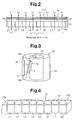
- Fig. 2 is a schematic cross-sectional view of an optical element according to a first embodiment of the present invention.
- Fig. 3 is a schematic perspective view of a deposition apparatus used in manufacturing the optical element in Fig. 2.
- Fig. 4 is a schematic perspective view of a rod lens array of the optical element in Fig. 2.
- Fig. 5 is a graph showing the characteristic of a multi-layered film filter of the optical element in Fig. 2.
- Fig. 6 is a graph showing a change in the center wavelength of the multi-layered film filter with respect to the rod lens array in Fig. 4.
- Fig. 7 is a schematic cross-sectional view of an optical element according to a second embodiment of the present invention.
- Fig. 8 is a schematic cross-sectional view of an optical element according to a third embodiment of the present invention.
- Fig. 9 is a schematic cross-sectional view of an optical element according to a fourth embodiment of the present invention.
- Fig. 10 is a schematic perspective view of a planar microlens of the optical element in Fig. 9.
- Fig. 11 is a schematic perspective view of another example of the planar microlens of the optical element in Fig. 9.
- Fig. 12 is a schematic perspective view of a film thickness correcting plate.
- Fig. 13 is a schematic perspective view of a further example of the planar microlens of the optical element in Fig. 9.
- Fig. 2 is a cross-sectional view schematically illustrating an optical element 11A according to the first embodiment of the present invention.
- the optical element 11A as shown in Fig. 2, includes a rod lens array 12 and a multi-layered film filter 13.
- the multi-layered film filter 13 is formed by alternately laminating high refractive-index dielectric layers and low refractive-index dielectric layers on one end face 14 of the rod lens array 12 in a lengthwise direction.
- the rod lens array 12 includes plural (eight in this embodiment) rod lenses L1 to L8.
- the rod lenses L1-L8 are gradient index optical elements and are arranged side by side in such a way that the optical axes of the adjoining rod lenses become in parallel.
- a resin is filled in gaps between and around the individual rod lenses L1-L8, and the rod lens array 12 is integrated by a holding plate (not shown).
- the one end face 14 of the rod lens array 12 in the lengthwise direction is flat.
- the multi-layered film filter 13 is formed on the entire surface of the one end face 14 of the rod lens array 12 in such a way that its thickness continuously changes in accordance with the positions of the individual rod lenses L1-L8.
- the film thickness of the multi-layered film filter 13 linearly increases from one end 14a of the rod lens array 12 to the other end 14b in the layout direction of the rod lenses L1-L8. That is, the thickness of the multi-layered film filter 13 increases toward the other end 14b of the rod lens array 12 from one end 14a. Therefore, the center wavelength of light which passes through the individual portions of the multi-layered film filter 13 becomes shorter as the thickness of the multi-layered film filter 13 becomes thinner. As shown in Fig. 2, the center wavelengths ( ⁇ 1 to ⁇ 8) of lights which pass the multi-layered film filter 13 at portions corresponding to the rod lenses L1-L8 are different.
- Fig. 5 shows the relationship between the wavelengths of the individual transmitted lights of the multi-layered film filter 13 and the transmittances.
- Fig. 5 shows the characteristic in a case where the multi-layered film filter 13 is an edge filter.
- the horizontal scale indicates the rod lenses L1-L8 as serial numbers 1 to 8 of the lenses
- the vertical scale indicates the ratios of the center wavelengths of other rod lenses L2-L8 to the center wavelength of the lens 1 (rod lens L1).
- the ratio of the center wavelength of the lens 3 (rod lens L3) to the center wavelength of the lens 1 is approximately 1.04 and the ratio of the center wavelength of the lens 6 (rod lens L6) to the center wavelength of the lens 1 is approximately 1.10.
- the multi-layered film filter 13 is a narrow-band filter or an edge filter formed by alternately laminating high refractive-index dielectric layers and low refractive-index dielectric layers, and is directly deposited on one end face 14 of the rod lens array 12 in vacuum by a physical vapor deposition method.
- a tantalum oxide is used for the high refractive-index dielectric layers and a silicon oxide is used for the low refractive-index dielectric layers.
- the multi-layered film filter 13 is deposited by sputtering (physical vapor deposition method) by using a deposition apparatus 15, for example, as shown in Fig. 3.
- a target 17 is attached to a target electrode 18 in a vacuum chamber 16 in the deposition apparatus 15.
- a negative voltage is applied to the target electrode 18 by a DC voltage source or an AC voltage source or a pulse voltage source.
- a vacuum exhaust system (not shown) is attached to the vacuum chamber 16.
- a single or plural rod lens arrays 12 are fixed at approximately equal intervals to the outer surface of a rotary drum 19 provided in the vacuum chamber 16.
- Fig. 3 shows a single rod lens array 12.
- Each rod lens array 12 is fixed to the outer surface of the rotary drum 19 in such a way that its lengthwise-directional one end face 14 faces the target 17 in a state inclined by an angle ⁇ with respect to the target 17.
- a negative voltage is applied to the target electrode 18 with an inactive gas of, for example, Ar fed into the chamber 16. Then, a plasma is produced in the vapor near the surface of the target electrode 18, and target atoms are emitted from the surface of the target electrode 18 by the sputtering phenomenon. The emitted target atoms are adhered and deposited on the one end face 14 of the rod lens array 12, thereby forming a thin film.
- a step of forming a thin film on the one end face 14 of the rod lens array 12 in this manner the rotary drum 19 is rotated at a predetermined speed and the one end face 14 of each rod lens array 12 passes in front of the target 17 in an inclined state. Accordingly, the distance between the one end face 14 and the target 17 (hereinafter called a target-array distance) becomes shorter toward the other end 14b from the one end 14a of the rod lens array 12. Therefore, the film that is formed on the one end face 14 becomes thicker toward the other end 14b from the one end 14a.
- the thickness of the multi-layered film filter 13 that is formed on the one end face 14 of the rod lens array 12 in this manner increases linearly toward the other end (second end) 14b from the one end (first end) 14a of the rod lens array 12 (see Fig. 2) in the layout direction of the individual rod lenses L1 to L8.
- the multi-layered film filter 13 can be deposited by, besides the sputtering method, vacuum deposition or other sputtering methods as the physical vapor deposition method.
- magnetron sputtering, ion beam sputtering and ion assist vapor deposition can be used.
- the optical element 11A of the first embodiment has the following advantages.
- Fig. 7 is a cross-sectional view schematically showing an optical element 11B according to the second embodiment of the present invention.
- the optical element 11B includes a laser diode array (light emitting device) 30 which emits light toward to the multi-layered film filter 13 via the individual rod lenses L1-L8 of the rod lens array 12 in addition to the structure of the optical element 11A of the first embodiment.
- the laser diode array 30 is provided on an other end face 24 facing the one end face 14 of the rod lens array 12 and integrated with the rod lens array 12.
- the laser diode array 30 has eight laser diodes (a plurality of light sources) LD1 to LD8 provided in association with the individual rod lenses L1-L8.
- the individual laser diodes LD1-LD8 emit laser lights of, for example, the same center wavelength.
- the half-value widths of the laser lights from the individual laser diodes LD1-LD8 may be wide. That is, according to the second embodiment, light having eight types of wavelengths ⁇ 1 to ⁇ 8 is demultiplexed by the multi-layered film filter 13 within the wavelength range of the half-value widths of the individual laser diodes LD1-LD8.
- the multi-layered film filter 13 is constructed as a narrow-band filter.
- the laser light to be output from the laser diode LD1 is made parallel by the rod lens L1 and enters the multi-layered film filter 13. Of the laser lights incident to the multi-layered film filter 13, the light that has a center wavelength of ⁇ 1 passes through the multi-layered film filter 13. Likewise, the laser lights to be output from the laser diodes LD2-LD8 are made parallel by the rod lenses L2-L8 respectively and the lights that respectively have center wavelengths of ⁇ 2- ⁇ 8 pass through the multi-layered film filter 13.
- the optical element 11B of the second embodiment has the following advantages.
- Fig. 8 is a cross-sectional view schematically showing an optical element 11C according to the third embodiment of the invention.
- the optical element 11C includes a photodetector array 40 in addition to the structure of the optical element 11A of the first embodiment.
- the photodetector array 40 detects a plurality of lights (lights with wavelengths ⁇ 1- ⁇ 8), demultiplexed by the multi-layered film filter 13, via the individual rod lenses L1-L8 of the rod lense array 12.
- the photodetector array 40 is provided on the other end face 24 facing the one end face 14 of the rod lens array 12 and is integrated with the rod lens array 12.
- the photodetector array 40 has eight photodetectors PD1 to PD8 provided in association with the rod lenses L1-L8.
- the multi-layered film filter 13 is constructed as a narrow-band filter.
- the optical element 11C of the third embodiment has the following advantages.
- Fig. 9 is a cross-sectional view schematically showing an optical element 11D according to the fourth embodiment of the present invention.
- Fig. 10 is a schematic perspective view of a planar microlens 50 of the optical element 11D.
- the optical element 11D has a gradient index planar microlens 50 in place of the rod lens array 12 of the first embodiment shown in Fig. 2.
- the planar microlens 50 has, for example, six microlenses 51 to 56, which are graded-index areas, on a single substrate 59. As shown in Figs. 9 and 10, a lengthwise-directional one end face 50a of the microlens 50 is formed as a flat face and the multi-layered film filter 13 is formed on that one end face 50a.
- the optical element 11D of the fourth embodiment has the same advantages as the first embodiment.
- the number of rod lenses of the rod lens array 12 is not limited to eight. A plurality of rod lenses may be laid out in two or more rows.
- the multi-layered film filter 13 may be formed via a film thickness correcting plate 70 (see Fig. 12) provided, for example, between the rod lens array 12 and the target 17.
- the film thickness correcting plate 70 has a substantially trapezoidal opening portion (71). In this case, a part of the surface of the target 17 which is exposed with respect to the one end face 14 is shielded by the film thickness correcting plate 70.
- the opening portion (71) is formed in a substantially trapezoidal shape and is formed in such a way that the width of the opening portion changes gradually toward the other end from the lengthwise-directional one end of the one end face 14 of the rod lens array 12.
- the target 17 and the rod lens array 12 are arranged in such a way that their lengthwise directions become the same. Therefore, the multi-layered film filter which has a film thickness according to the exposed width (the width of the opening portion) of the surface of the target 17 is formed on the lengthwise-directional one end face 14 of the rod lens array 12.
- the film thickness correcting plate 70 may be provided between the lens array 12 and an evaporation source.
- an LED array may be used as the light emitting device.
- the multi-layered film filter 13 may be formed on an other end face 50b facing the one end face 50a of the gradient index planar microlens 50.
- a gradient index planar microlens 50' shown in Fig. 11 may be used in the optical element 11D.
- Six microlenses 51' to 56' which are graded-index areas are formed in a semicolumnar shape on the substrate 59 of the microlens 50'.
- the multi-layered film filter 13 is formed on one of both end faces 50a', 50b' of the substrate 59. Both end faces 50a', 50b' are formed flat.
- a gradient index planar microlens 60 shown in Fig. 13 may be used in the optical element 11D.
- six substantially hemispherical microlenses 61 to 66 are protrusively formed on one end face 60a of a substrate 69 of the planar microlens 60.
Landscapes
- Physics & Mathematics (AREA)
- General Physics & Mathematics (AREA)
- Optics & Photonics (AREA)
- Optical Couplings Of Light Guides (AREA)
- Semiconductor Lasers (AREA)
- Light Receiving Elements (AREA)
- Optical Filters (AREA)
Abstract
An optical element having wavelength selectivity,
which is easy to manufacture and reduces the manufacturing
cost. The optical element comprises a lens array (12)
having one end face and a plurality of lenses (L1-L8)
arranged on the one end face, and a multi-layered film
filter (13) formed on the one end face (14) of the lens
array. The multi-layered film filter includes high
refractive-index dielectric layers and low refractive-index
dielectric layers laminated alternately and its film
thickness continuously changes in accordance with positions
of the individual lenses. The center wavelength of
transmitted light from the multi-layered film filter varies
in accordance with the position of the lens array. In a
case where mixed light enters the multi-layered film filter
from the individual lenses, the mixed light is
demultiplexed into lights of different center wavelengths
by the multi-layered film filter that has difference
thicknesses.
Description
The present invention relates to an optical element
having wavelength selectivity, and, more particularly, to
an optical element which multiplexes lights of different
wavelengths or demultiplexes multiplexed light wavelength
by wavelength.
Optical elements using an optical fiber and
collimator lens have conventionally been used as optical
communication equipment parts. When optical communication
becomes very popular from now on, miniaturization and
integration of optical communication equipment parts become
further essential. Optical communication requires a
technique which demultiplexes light by selectively
transmitting or reflecting light wavelength by wavelength.
A multi-layered film filter which has high refractive-index
dielectric layers and low refractive-index dielectric
layers alternately laminated, e.g., an edge filter or a
narrow-band filter, is known as an optical filter.
An optical communication equipment part 100 as shown
in, for example, Fig. 1 is known as a conventional optical
communication equipment part which uses such an optical
filter. The optical communication equipment part 100
demultiplexes mixed light including eight kinds of optical
signals (Ch1-8) with different center wavelengths into
individual optical signals.
As shown in Fig. 1, the optical communication
equipment part 100 includes a plurality of collimator
lenses 101, 102, 104 to 119, an attenuator 103 and a
plurality of optical filters F1 to F9. Each of the
collimator lenses 101, 102, 104-119 is constituted by a rod
lens, and the attenuator 103 attenuates the light intensity
of incident light to a predetermined value. An optical
signal is sent among those members through an optical fiber.
Mixed light which has entered the optical
communication equipment part 100 is first separated into
transmitted light (optical signal Ch5) and reflected light
(optical signals Ch1-4, 6-8) by the optical filter F5. The
optical signal Ch5 is let out after its light intensity is
attenuated to a predetermined value by the attenuator 103.
The optical signals Ch1-4, 6-8 are separated into
transmitted light (optical signals Ch6-8) and reflected
light (optical signals Ch1-4) by the optical filter F9.
The optical signals Ch6-8 are separated into transmitted
light (optical signal Ch6) and reflected light (optical
signals Ch7, 8) by the optical filter F6. The optical
signal Ch6 is let out through the collimator lens 107.
Meanwhile, the optical signals Ch7, 8 are separated into
transmitted light (optical signal Ch7) and reflected light
(optical signal Ch8) by the optical filter F7. The optical
signal Ch7 is let out through the collimator lens 109, and
the optical signal Ch8 passes through the optical filter F8
and is let out through the collimator lens 111.
The optical signals Ch1-4 as reflected light from the
optical filter F9 are separated into transmitted light
(optical signal Ch1) and reflected light (optical signals
Ch2-4) by the optical filter F1, and the optical signal Ch1
is let out through the collimator lens 113. The optical
signals Ch2-4 are separated into transmitted light (optical
signal Ch2) and reflected light (optical signals Ch3, 4) by
the optical filter F2, and the optical signal Ch2 is let
out through the collimator lens 115. The optical signals
Ch3, 4 are separated into transmitted light (optical signal
Ch3) and reflected light (optical signal Ch4) by the
optical filter F3. Ch3 is let out through the collimator
lens 117, and the optical signal Ch4 passes through the
optical filter F4 and is let out through the collimator
lens 119.
The prior art technique illustrated in Fig. 1 has the
following problems.
Paying attention to the conventional problems, the
present invention has been made and aims at providing an
optical element having wavelength selectivity, which is
easy to manufacture and reduces the manufacturing cost.
To achieve the above-described object, according to a
first aspect of the present invention, there is provided an
optical element having wavelength selectivity, comprising a
lens array having one end face and a plurality of lenses
arranged on the one end face; and a multi-layered film
filter formed on the one end face of the lens array. The
multi-layered film filter includes high refractive-index
dielectric layers and low refractive-index dielectric
layers laminated alternately and its film thickness
continuously changes in accordance with positions of the
individual lenses.
It is preferable that the plurality of lenses should
be aligned in a line toward a second end from a first end
of the one end face of the lens array and the thickness of
the multi-layered film filter should linearly change toward
the second end from the first end.
It is preferable that the lens array should be a rod
lens array including a plurality of rod lenses.
It is preferable that the lens array should be a
gradient index planar microlens including a single
substrate and a plurality of microlenses formed in a line
on the substrate.
It is preferable that the plurality of microlenses
should protrude from the substrate.
It is preferable that the lens array should have
another end face facing the one end face; and the optical
element should further have a light emitting device for
emitting light toward the multi-layered film filter via
individual lenses of the lens array.
It is preferable that the light emitting device
should be integral with the lens array.
It is preferable that the light emitting device
should include a plurality of light sources provided in
association with individual lenses of the lens array.
It is preferable that the lens array should have
another end face facing the one end face; and the optical
element should further have a plurality of light receiving
elements for respectively receiving a plurality of optical
signals having different center wavelengths, obtained by
demultiplexing incident light by the multi-layered film
filter, via individual lenses of the lens array.
It is preferable that the plurality of light
receiving elements is integral with the lens array.
According to a second aspect of the present invention,
there is provided a method of manufacturing an optical
element having wavelength selectivity. The manufacturing
method comprises a step of preparing a lens array having
one end face and a plurality of lenses arranged on the one
end face; and a step of directly forming a multi-layered
film filter on the one end face of the lens array by a
physical vapor deposition method in such a way that a
thickness continuously changes in accordance with positions
of the plurality of individual lenses.
It is preferable that the manufacturing method should
further comprise a step of arranging the lens array in such
a way that the one end face of the lens array is inclined
with respect to an evaporation source or a target, prior to
the step of forming the multi-layered film filter.
It is preferable that the manufacturing method should
further comprise a step of arranging a film thickness
correcting plate having a substantially trapezoidal opening
portion between the lens array and the evaporation source
or target, prior to the step of forming the multi-layered
film filter.
To better understand the present invention together
with the object and features of the present invention, the
following description of representative embodiments
together with the accompanying drawings will be referred to.
Fig. 1 is a schematic connection diagram of a
conventional optical element.
Fig. 2 is a schematic cross-sectional view of an
optical element according to a first embodiment of the
present invention.
Fig. 3 is a schematic perspective view of a
deposition apparatus used in manufacturing the optical
element in Fig. 2.
Fig. 4 is a schematic perspective view of a rod lens
array of the optical element in Fig. 2.
Fig. 5 is a graph showing the characteristic of a
multi-layered film filter of the optical element in Fig. 2.
Fig. 6 is a graph showing a change in the center
wavelength of the multi-layered film filter with respect to
the rod lens array in Fig. 4.
Fig. 7 is a schematic cross-sectional view of an
optical element according to a second embodiment of the
present invention.
Fig. 8 is a schematic cross-sectional view of an
optical element according to a third embodiment of the
present invention.
Fig. 9 is a schematic cross-sectional view of an
optical element according to a fourth embodiment of the
present invention.
Fig. 10 is a schematic perspective view of a planar
microlens of the optical element in Fig. 9.
Fig. 11 is a schematic perspective view of another
example of the planar microlens of the optical element in
Fig. 9.
Fig. 12 is a schematic perspective view of a film
thickness correcting plate.
Fig. 13 is a schematic perspective view of a further
example of the planar microlens of the optical element in
Fig. 9.
Fig. 2 is a cross-sectional view schematically
illustrating an optical element 11A according to the first
embodiment of the present invention. The optical element
11A, as shown in Fig. 2, includes a rod lens array 12 and a
multi-layered film filter 13. The multi-layered film
filter 13 is formed by alternately laminating high
refractive-index dielectric layers and low refractive-index
dielectric layers on one end face 14 of the rod lens array
12 in a lengthwise direction.
As shown in Fig. 4, the rod lens array 12 includes
plural (eight in this embodiment) rod lenses L1 to L8. The
rod lenses L1-L8 are gradient index optical elements and
are arranged side by side in such a way that the optical
axes of the adjoining rod lenses become in parallel. A
resin is filled in gaps between and around the individual
rod lenses L1-L8, and the rod lens array 12 is integrated
by a holding plate (not shown). The one end face 14 of the
rod lens array 12 in the lengthwise direction is flat.
The multi-layered film filter 13 is formed on the
entire surface of the one end face 14 of the rod lens array
12 in such a way that its thickness continuously changes in
accordance with the positions of the individual rod lenses
L1-L8. Specifically, the film thickness of the multi-layered
film filter 13 linearly increases from one end 14a
of the rod lens array 12 to the other end 14b in the layout
direction of the rod lenses L1-L8. That is, the thickness
of the multi-layered film filter 13 increases toward the
other end 14b of the rod lens array 12 from one end 14a.
Therefore, the center wavelength of light which passes
through the individual portions of the multi-layered film
filter 13 becomes shorter as the thickness of the multi-layered
film filter 13 becomes thinner. As shown in Fig. 2,
the center wavelengths (λ1 to λ8) of lights which pass the
multi-layered film filter 13 at portions corresponding to
the rod lenses L1-L8 are different.
Fig. 5 shows the relationship between the wavelengths
of the individual transmitted lights of the multi-layered
film filter 13 and the transmittances. Fig. 5 shows the
characteristic in a case where the multi-layered film
filter 13 is an edge filter. In Fig. 6, the horizontal
scale indicates the rod lenses L1-L8 as serial numbers 1 to
8 of the lenses, and the vertical scale indicates the
ratios of the center wavelengths of other rod lenses L2-L8
to the center wavelength of the lens 1 (rod lens L1). For
example, the ratio of the center wavelength of the lens 3
(rod lens L3) to the center wavelength of the lens 1 is
approximately 1.04 and the ratio of the center wavelength
of the lens 6 (rod lens L6) to the center wavelength of the
lens 1 is approximately 1.10.
The multi-layered film filter 13 is a narrow-band
filter or an edge filter formed by alternately laminating
high refractive-index dielectric layers and low refractive-index
dielectric layers, and is directly deposited on one
end face 14 of the rod lens array 12 in vacuum by a
physical vapor deposition method. Here, for example, a
tantalum oxide is used for the high refractive-index
dielectric layers and a silicon oxide is used for the low
refractive-index dielectric layers.
The multi-layered film filter 13 is deposited by
sputtering (physical vapor deposition method) by using a
deposition apparatus 15, for example, as shown in Fig. 3.
A target 17 is attached to a target electrode 18 in a
vacuum chamber 16 in the deposition apparatus 15. A
negative voltage is applied to the target electrode 18 by a
DC voltage source or an AC voltage source or a pulse
voltage source. A vacuum exhaust system (not shown) is
attached to the vacuum chamber 16. A single or plural rod
lens arrays 12 are fixed at approximately equal intervals
to the outer surface of a rotary drum 19 provided in the
vacuum chamber 16. Fig. 3 shows a single rod lens array 12.
Each rod lens array 12 is fixed to the outer surface
of the rotary drum 19 in such a way that its lengthwise-directional
one end face 14 faces the target 17 in a state
inclined by an angle α with respect to the target 17.
After the internal space of the vacuum chamber 16 is
set to a high vacuum state by the vacuum exhaust system, a
negative voltage is applied to the target electrode 18 with
an inactive gas of, for example, Ar fed into the chamber 16.
Then, a plasma is produced in the vapor near the surface of
the target electrode 18, and target atoms are emitted from
the surface of the target electrode 18 by the sputtering
phenomenon. The emitted target atoms are adhered and
deposited on the one end face 14 of the rod lens array 12,
thereby forming a thin film.
In a step of forming a thin film on the one end face
14 of the rod lens array 12 in this manner, the rotary drum
19 is rotated at a predetermined speed and the one end face
14 of each rod lens array 12 passes in front of the target
17 in an inclined state. Accordingly, the distance between
the one end face 14 and the target 17 (hereinafter called a
target-array distance) becomes shorter toward the other end
14b from the one end 14a of the rod lens array 12.
Therefore, the film that is formed on the one end face 14
becomes thicker toward the other end 14b from the one end
14a. The thickness of the multi-layered film filter 13
that is formed on the one end face 14 of the rod lens array
12 in this manner increases linearly toward the other end
(second end) 14b from the one end (first end) 14a of the
rod lens array 12 (see Fig. 2) in the layout direction of
the individual rod lenses L1 to L8.
Note that the multi-layered film filter 13 can be
deposited by, besides the sputtering method, vacuum
deposition or other sputtering methods as the physical
vapor deposition method. To acquire a high weather
resistance by the multi-layered film filter 13, magnetron
sputtering, ion beam sputtering and ion assist vapor
deposition can be used.
The optical element 11A of the first embodiment has
the following advantages.
Fig. 7 is a cross-sectional view schematically
showing an optical element 11B according to the second
embodiment of the present invention. The optical element
11B includes a laser diode array (light emitting device) 30
which emits light toward to the multi-layered film filter
13 via the individual rod lenses L1-L8 of the rod lens
array 12 in addition to the structure of the optical
element 11A of the first embodiment. The laser diode array
30 is provided on an other end face 24 facing the one end
face 14 of the rod lens array 12 and integrated with the
rod lens array 12. The laser diode array 30 has eight
laser diodes (a plurality of light sources) LD1 to LD8
provided in association with the individual rod lenses L1-L8.
The individual laser diodes LD1-LD8 emit laser lights
of, for example, the same center wavelength. The half-value
widths of the laser lights from the individual laser
diodes LD1-LD8 may be wide. That is, according to the
second embodiment, light having eight types of wavelengths
λ1 to λ8 is demultiplexed by the multi-layered film filter
13 within the wavelength range of the half-value widths of
the individual laser diodes LD1-LD8. The multi-layered
film filter 13 is constructed as a narrow-band filter.
The laser light to be output from the laser diode LD1
is made parallel by the rod lens L1 and enters the multi-layered
film filter 13. Of the laser lights incident to
the multi-layered film filter 13, the light that has a
center wavelength of λ1 passes through the multi-layered
film filter 13. Likewise, the laser lights to be output
from the laser diodes LD2-LD8 are made parallel by the rod
lenses L2-L8 respectively and the lights that respectively
have center wavelengths of λ2-λ8 pass through the multi-layered
film filter 13.
The optical element 11B of the second embodiment has
the following advantages.
Fig. 8 is a cross-sectional view schematically
showing an optical element 11C according to the third
embodiment of the invention. The optical element 11C
includes a photodetector array 40 in addition to the
structure of the optical element 11A of the first
embodiment. The photodetector array 40 detects a plurality
of lights (lights with wavelengths λ1-λ8), demultiplexed by
the multi-layered film filter 13, via the individual rod
lenses L1-L8 of the rod lense array 12. The photodetector
array 40 is provided on the other end face 24 facing the
one end face 14 of the rod lens array 12 and is integrated
with the rod lens array 12. The photodetector array 40 has
eight photodetectors PD1 to PD8 provided in association
with the rod lenses L1-L8. The multi-layered film filter
13 is constructed as a narrow-band filter.
The optical element 11C of the third embodiment has
the following advantages.
Fig. 9 is a cross-sectional view schematically
showing an optical element 11D according to the fourth
embodiment of the present invention. Fig. 10 is a
schematic perspective view of a planar microlens 50 of the
optical element 11D. The optical element 11D has a
gradient index planar microlens 50 in place of the rod lens
array 12 of the first embodiment shown in Fig. 2.
The planar microlens 50 has, for example, six
microlenses 51 to 56, which are graded-index areas, on a
single substrate 59. As shown in Figs. 9 and 10, a
lengthwise-directional one end face 50a of the microlens 50
is formed as a flat face and the multi-layered film filter
13 is formed on that one end face 50a.
The optical element 11D of the fourth embodiment has
the same advantages as the first embodiment.
It should be apparent to those skilled in the art
that the present invention may be embodied in other
substituting examples without departing from the spirit and
scope of the present invention.
In the first embodiment, the number of rod lenses of
the rod lens array 12 is not limited to eight. A plurality
of rod lenses may be laid out in two or more rows.
In the first embodiment, the multi-layered film
filter 13 may be formed via a film thickness correcting
plate 70 (see Fig. 12) provided, for example, between the
rod lens array 12 and the target 17. The film thickness
correcting plate 70 has a substantially trapezoidal opening
portion (71). In this case, a part of the surface of the
target 17 which is exposed with respect to the one end face
14 is shielded by the film thickness correcting plate 70.
Specifically, the opening portion (71) is formed in a
substantially trapezoidal shape and is formed in such a way
that the width of the opening portion changes gradually
toward the other end from the lengthwise-directional one
end of the one end face 14 of the rod lens array 12. The
target 17 and the rod lens array 12 are arranged in such a
way that their lengthwise directions become the same.
Therefore, the multi-layered film filter which has a film
thickness according to the exposed width (the width of the
opening portion) of the surface of the target 17 is formed
on the lengthwise-directional one end face 14 of the rod
lens array 12. That is, the film thickness of the multi-layered
film filter which faces a portion at which the
width of the opening of the surface of the target 17 is
narrow is thin, and the film thickness of the multi-layered
film filter which faces a portion at which the width of the
opening is wide is thick. The film thickness correcting
plate 70 may be provided between the lens array 12 and an
evaporation source.
In the second embodiment, an LED array may be used as
the light emitting device.
In the fourth embodiment, the multi-layered film
filter 13 may be formed on an other end face 50b facing the
one end face 50a of the gradient index planar microlens 50.
In the fourth embodiment, a gradient index planar
microlens 50' shown in Fig. 11 may be used in the optical
element 11D. Six microlenses 51' to 56' which are graded-index
areas are formed in a semicolumnar shape on the
substrate 59 of the microlens 50'. In this case, the
multi-layered film filter 13 is formed on one of both end
faces 50a', 50b' of the substrate 59. Both end faces 50a',
50b' are formed flat.
In the fourth embodiment, a gradient index planar
microlens 60 shown in Fig. 13 may be used in the optical
element 11D. For example, six substantially hemispherical
microlenses 61 to 66 are protrusively formed on one end
face 60a of a substrate 69 of the planar microlens 60.
Claims (13)
- An optical element having wavelength selectivity, characterized by:a lens array having one end face and a plurality of lenses (L1-L8) arranged on the one end face; anda multi-layered film filter (13) which is formed on the one end face (14) of the lens array and includes high refractive-index dielectric layers and low refractive-index dielectric layers laminated alternately and whose film thickness continuously changes in accordance with positions of the individual lenses.
- The optical element according to Claim 1, characterized in that the plurality of lenses are aligned in a line toward a second end from a first end of the one end face of the lens array and the film thickness of the multi-layered film filter linearly changes toward the second end from the first end.
- The optical element according to Claim 1 or 2, characterized in that the lens array is a rod lens array including a plurality of rod lenses.
- The optical element according to Claim 1 or 2, characterized in that the lens array is a gradient index planar microlens (50, 60) including a single substrate (59, 69) and a plurality of microlenses (51-56, 61-66) formed in a line on the substrate.
- The optical element according to Claim 4, characterized in that the plurality of microlenses (61-66) protrude from the substrate.
- The optical element according to any one of Claims 1 to 5, characterized in that the lens array has an other end face (24) facing the one end face; and
the optical element further has a light emitting device (30) formed on the other end face for emitting light toward the multi-layered film filter via individual lenses of the lens array. - The optical element according to Claim 6, characterized in that the light emitting device is integral with the lens array.
- The optical element according to Claim 6 or 7, characterized in that the light emitting device includes a plurality of light sources (LD1-LD8) provided in association with individual lenses of the lens array.
- The optical element according to any one of Claims 1 to 5, characterized in that the lens array has an other end face facing the one end face; and
the optical element further has a plurality of light receiving elements (PD1-PD8) formed on the other end face for respectively receiving a plurality of optical signals having different center wavelengths, obtained by demultiplexing input light by the multi-layered film filter, via individual lenses of the lens array. - The optical element according to Claim 9, characterized in that the plurality of light receiving elements are integral with the lens array.
- A method of manufacturing an optical element having wavelength selectivity, characterized by:a step of preparing a lens array (12) having one end face and a plurality of lenses (L1-L8) arranged on the one end face; anda step of directly forming a multi-layered film filter on the one end face of the lens array by a physical vapor deposition method in such a way that the film thickness continuously changes in accordance with positions of the plurality of individual lenses.
- The optical element manufacturing method according to Claim 11, further characterized by:a step of arranging the lens array in such a way that the one end face of the lens array is inclined with respect to an evaporation source or a target, prior to the step of forming the multi-layered film filter.
- The optical element manufacturing method according to Claim 12, further characterized by:a step of arranging a film thickness correcting plate (70) having a substantially trapezoidal opening portion (71) between the lens array and the evaporation source or target, prior to the step of forming the multi-layered film filter.
Applications Claiming Priority (5)
| Application Number | Priority Date | Filing Date | Title |
|---|---|---|---|
| JP2000214379 | 2000-07-14 | ||
| JP2000214379 | 2000-07-14 | ||
| JP2000278268 | 2000-09-13 | ||
| JP2000278268A JP2002090523A (en) | 2000-07-14 | 2000-09-13 | Optical element with wavelength selectivity |
| PCT/JP2001/006010 WO2002006861A1 (en) | 2000-07-14 | 2001-07-11 | Optical element having wavelength selectivity |
Publications (1)
| Publication Number | Publication Date |
|---|---|
| EP1304585A1 true EP1304585A1 (en) | 2003-04-23 |
Family
ID=26596068
Family Applications (1)
| Application Number | Title | Priority Date | Filing Date |
|---|---|---|---|
| EP01949938A Withdrawn EP1304585A1 (en) | 2000-07-14 | 2001-07-11 | Optical element having wavelength selectivity |
Country Status (7)
| Country | Link |
|---|---|
| US (1) | US20020135878A1 (en) |
| EP (1) | EP1304585A1 (en) |
| JP (1) | JP2002090523A (en) |
| CN (1) | CN1386205A (en) |
| CA (1) | CA2384998A1 (en) |
| TW (1) | TW578017B (en) |
| WO (1) | WO2002006861A1 (en) |
Families Citing this family (8)
| Publication number | Priority date | Publication date | Assignee | Title |
|---|---|---|---|---|
| JP4657515B2 (en) * | 2001-08-01 | 2011-03-23 | 株式会社フジクラ | Method for manufacturing optical collimator component with dielectric multilayer film |
| CN101047463B (en) * | 2006-10-25 | 2012-05-23 | 浙江大学 | Multi-channel wavelength space decomplex film device based on two-end thickness decreasing structure |
| JP5659889B2 (en) * | 2011-03-11 | 2015-01-28 | セイコーエプソン株式会社 | Inclined structure and method for manufacturing spectroscopic sensor |
| US8841831B2 (en) * | 2012-03-13 | 2014-09-23 | Panasonic Corporation | Light emitting device, and illumination apparatus and luminaire using same |
| JP5701286B2 (en) * | 2012-12-28 | 2015-04-15 | 富士フイルム株式会社 | Liquid crystal display |
| CN111033319B (en) * | 2017-09-29 | 2022-03-04 | 日本电产株式会社 | Lens, lens unit, and image pickup apparatus |
| WO2020188676A1 (en) * | 2019-03-18 | 2020-09-24 | 三菱電機株式会社 | Lidar device and air conditioner |
| JP7275946B2 (en) * | 2019-07-10 | 2023-05-18 | セイコーエプソン株式会社 | Optical filters and electronics |
Family Cites Families (11)
| Publication number | Priority date | Publication date | Assignee | Title |
|---|---|---|---|---|
| JPS55155204U (en) * | 1979-04-24 | 1980-11-08 | ||
| JPS5945408A (en) * | 1982-09-08 | 1984-03-14 | Ulvac Corp | Production of optical filter |
| JPS59104603A (en) * | 1982-12-08 | 1984-06-16 | Hoya Corp | Beam splitter |
| US5872655A (en) * | 1991-07-10 | 1999-02-16 | Optical Coating Laboratory, Inc. | Monolithic linear variable filter and method of manufacture |
| JPH0749417A (en) * | 1993-08-06 | 1995-02-21 | Fujitsu Ltd | Interference filter assembly |
| JP2000505595A (en) * | 1996-02-13 | 2000-05-09 | オプティカル コーポレーション オブ アメリカ | External cavity semiconductor laser with monolithic prism assembly |
| US5835517A (en) * | 1996-10-04 | 1998-11-10 | W. L. Gore & Associates, Inc. | WDM multiplexer-demultiplexer using Fabry-Perot filter array |
| US6054703A (en) * | 1998-03-20 | 2000-04-25 | Syscan, Inc. | Sensing module for accelerating signal readout from image sensors |
| US6064522A (en) * | 1998-06-23 | 2000-05-16 | Lucent Technologies Inc | Miniature mass producible non-reciprocal devices |
| US6057925A (en) * | 1998-08-28 | 2000-05-02 | Optical Coating Laboratory, Inc. | Compact spectrometer device |
| US6542306B2 (en) * | 2001-03-16 | 2003-04-01 | Optical Coating Laboratories, Inc. | Compact multiple channel multiplexer/demultiplexer devices |
-
2000
- 2000-09-13 JP JP2000278268A patent/JP2002090523A/en active Pending
-
2001
- 2001-07-11 CA CA002384998A patent/CA2384998A1/en not_active Abandoned
- 2001-07-11 EP EP01949938A patent/EP1304585A1/en not_active Withdrawn
- 2001-07-11 CN CN01802031A patent/CN1386205A/en active Pending
- 2001-07-11 US US10/070,708 patent/US20020135878A1/en not_active Abandoned
- 2001-07-11 WO PCT/JP2001/006010 patent/WO2002006861A1/en not_active Ceased
- 2001-07-12 TW TW090117158A patent/TW578017B/en not_active IP Right Cessation
Non-Patent Citations (1)
| Title |
|---|
| See references of WO0206861A1 * |
Also Published As
| Publication number | Publication date |
|---|---|
| US20020135878A1 (en) | 2002-09-26 |
| TW578017B (en) | 2004-03-01 |
| JP2002090523A (en) | 2002-03-27 |
| WO2002006861A1 (en) | 2002-01-24 |
| CA2384998A1 (en) | 2002-01-24 |
| CN1386205A (en) | 2002-12-18 |
Similar Documents
| Publication | Publication Date | Title |
|---|---|---|
| EP1336873A1 (en) | Optical element having wavelength selectivity | |
| KR100271565B1 (en) | Wavelength demultiplexer and manufacturing method thereof | |
| US20140133862A1 (en) | Receiver optical module installing optical demultiplexer and method to produce optical demultiplexer | |
| CN104348083B (en) | wavelength monitor and optical module | |
| JP2020021013A (en) | WDM optical module, WDM optical module, and optical module | |
| US9391709B2 (en) | Optical transmitter module | |
| US9772449B2 (en) | Wavelength multiplexer/demultiplexer and optical module | |
| US20160187585A1 (en) | Optical fitler subassembly for compact wavelength demultiplexing device | |
| US9720190B2 (en) | Optical module and method for manufacturing optical module | |
| US20110026123A1 (en) | Wavelength-division apparatus and wavelength combining apparatus | |
| US7215885B2 (en) | Wavelength division element and optical module | |
| JP2010191231A (en) | Optical module | |
| US20180275347A1 (en) | Compact structure of integrated WDM device | |
| US20020135878A1 (en) | Optical element having wavelength selectivity | |
| US20040208452A1 (en) | Arrangement for multiplexing and/or demultiplexing optical signals having a plurality of wavelengths | |
| JP5983479B2 (en) | Optical element | |
| US20030002101A1 (en) | Device and method for multiplexing and/or demultiplexing optical signals of a plurality of wavelengths | |
| WO2002006872A1 (en) | Optical waveguide device having wavelength selectivity | |
| JP2017097072A (en) | Optical splitter, and optical receiver module, and manufacturing method thereof | |
| US7738750B2 (en) | Compact, low-loss optical wavelength multiplexer/demultiplexer | |
| CN111812778A (en) | Multiplexing and demultiplexing device | |
| US6816643B2 (en) | Wavelength tunable demultiplexing filter device, wavelength tunable multiplexing filter device, and wavelength routing device | |
| KR20140107747A (en) | Wavelength Division Multiplexer using Planar optical waveguide and Thin film filter | |
| JP2014123054A (en) | Optical module | |
| CN115480348A (en) | Integrated light source module |
Legal Events
| Date | Code | Title | Description |
|---|---|---|---|
| PUAI | Public reference made under article 153(3) epc to a published international application that has entered the european phase |
Free format text: ORIGINAL CODE: 0009012 |
|
| 17P | Request for examination filed |
Effective date: 20030110 |
|
| AK | Designated contracting states |
Designated state(s): AT BE CH CY DE DK ES FI FR GB GR IE IT LI LU MC NL PT SE TR |
|
| AX | Request for extension of the european patent |
Extension state: AL LT LV MK RO SI |
|
| STAA | Information on the status of an ep patent application or granted ep patent |
Free format text: STATUS: THE APPLICATION HAS BEEN WITHDRAWN |
|
| 18W | Application withdrawn |
Effective date: 20030613 |