EP1303829B1 - Miniature sensor chip, especially for fingerprint sensors - Google Patents
Miniature sensor chip, especially for fingerprint sensors Download PDFInfo
- Publication number
- EP1303829B1 EP1303829B1 EP01938854A EP01938854A EP1303829B1 EP 1303829 B1 EP1303829 B1 EP 1303829B1 EP 01938854 A EP01938854 A EP 01938854A EP 01938854 A EP01938854 A EP 01938854A EP 1303829 B1 EP1303829 B1 EP 1303829B1
- Authority
- EP
- European Patent Office
- Prior art keywords
- electrically conductive
- conductive layer
- sensor
- sensor chip
- layer
- Prior art date
- Legal status (The legal status is an assumption and is not a legal conclusion. Google has not performed a legal analysis and makes no representation as to the accuracy of the status listed.)
- Expired - Lifetime
Links
Images

Classifications
-
- G—PHYSICS
- G06—COMPUTING OR CALCULATING; COUNTING
- G06V—IMAGE OR VIDEO RECOGNITION OR UNDERSTANDING
- G06V40/00—Recognition of biometric, human-related or animal-related patterns in image or video data
- G06V40/10—Human or animal bodies, e.g. vehicle occupants or pedestrians; Body parts, e.g. hands
- G06V40/12—Fingerprints or palmprints
- G06V40/1335—Combining adjacent partial images (e.g. slices) to create a composite input or reference pattern; Tracking a sweeping finger movement
-
- G—PHYSICS
- G06—COMPUTING OR CALCULATING; COUNTING
- G06V—IMAGE OR VIDEO RECOGNITION OR UNDERSTANDING
- G06V40/00—Recognition of biometric, human-related or animal-related patterns in image or video data
- G06V40/10—Human or animal bodies, e.g. vehicle occupants or pedestrians; Body parts, e.g. hands
- G06V40/12—Fingerprints or palmprints
- G06V40/13—Sensors therefor
- G06V40/1306—Sensors therefor non-optical, e.g. ultrasonic or capacitive sensing
Definitions
- This invention relates to a sensor chip, especially for measuring structures in a finger surface.
- Fingerprint sensors based on capacitive coupling of an AC signal from the groove pattern of the finger to an array (matrix) of sensor elements being known from international patent application WO 98/58342 .
- US patent 5,963,679 describes a similar sensor with a different measuring principle and a two dimensional sensor matrix.
- the senor For special applications, e.g. when being mounted in a cellular phone or a lap-top PC, it is important that the sensor is made as small and light as possible. Such a miniature sensor may also be made a very cost effective is production techniques suitable for mass production are used.
- Noise considerations are important when positioning the electronic interrogation circuit, often a costumer specified silicon circuit ("ASIC") as close to the capacitance sensitive elements in the sensor array as possible, so that the length of the electrical conductors between the silicon circuit and the sensor elements is minimized.
- ASIC costumer specified silicon circuit
- the object of this invention is to secure a cost effective and miniaturized sensor solution based on a naked silicon chip (ASIC) with a multi layer metallization having a surface defining the interface toward the users fingers.
- ASIC naked silicon chip
- the principle is based the fact that the array of imaging sensor elements is positioned in one of the upper metal layers on a silicon surface.
- the silicon surface is provided with a number of metal layers with conductor leads, being separated by thin dielectric layers.
- a so called sandwich structure with extra layers of metal and dielectrics on top of the other layers.
- the present invention relates to a simplified solution being characterized as disclosed in claim 1.
- the senor thus may be produced using standard processes for IC production, this will give a very cost efficient sensor being suitable for mass production.
- the sensor chip according to the invention preferably consists of a naked silicon chip 6 in a housing 7 without a cover (or possibly on a circuit board or ceramic substrate) with a number of layers of metal or another electrically conductive material such as polysilicon, and a dielectric constituting the interface toward the users fingers.
- the principle is based on imaging sensor elements constituting a part of the third or fourth upper layer of the electrically conductive layers 1 on the silicon circuit, and that the conductor leads, from the elements then is routed individually down to the amplifier circuits on the surface of the silicon chip.
- the present solution may be produced industrially by standard methods for ASIC production and packing, as the silicon chip is mounted in a ceramic or plastic based housing without a lid, or on a circuit board or a ceramic substrate.
- the silicon chip is coupled electrically to the circuit board or housing with so called wire bonding.
- the three or four upper metal layers on the ASIC must be used for different structures with a given electric function as for example illustrated in fig. 1 .
- the layers provided on the substrate shown in figures 1 and 2 shows examples of the construction of an the ASICs upper layers with metal and dielectric, respectively, and will be explained below.
- the process for realizing the metal and dielectric layers on the silicon chip is well known technology, but the functionality of the individual layers and the combination of these is covered by the present invention, especially aimed at fingerprint sensors, as a variant of the sensor described in international patent application WO98/58342 which comprises an essentially linear sensor array 8, as shown in figure 3 .
- Figures 2 and 3 also show secondary sensor groups which may be used for velocity calculations, as described in the abovementioned patent.
- a line shaped sensor has the great advantage that it needs far less room and less individual channels than a two dimensional sensor with the same resolution, so that it may be made at a much lower cost.
- the electrical layer 1 constitutes the imaging sensor elements 8.
- the sensor elements may be positioned as shown in figure 3 , as a variant of the patented solution in international patent application No PCT/N098/00182 .
- the dielectric layer 2, in figure 1 functions as an insulation layer between the conductor leads in the electrically conductive layer 1 and the earth plane in the electrically conductive layer 3.
- the layer also constitutes a part of the total dielectric thickness (insulation) between the finger and the sensor element.
- the electrically conductive layer 3 constitutes an earthed plane shielding the conductor leads etc against direct coupling of AC signal from the finger and from the modulation ring 5.
- the earthed layer 3 will preferably be shaped so as to cover all conductor leads on the underlying first electrically conductive layer 1, but must have windows over the sensor elements 8.
- the openings in the earth plane 3 over the sensor elements 8 contributes with a "lens" effect to shape the electric field and thus the capacitive coupling between the finger and the sensor elements, and the shape of the sensor element 8 and the opening in the second electrically conductive layer 3 may be optimized to maximize the signal strength without going on accord with the geometric resolution of the sensor.
- the earthed shielding structure may be made using two electrically conductive layers being insulated from each other by a dielectric layer. This will provide an improved shielding and lens effect compared to the use of one layer.
- the second dielectric layer 4 may insulate between the earth plane 3 and outer electrically conductive layer 5, and the second dielectric layer 4 functions as an AC coupling of the signal to the electronics.
- the layer 4 also constitutes (as mentioned above) a part of the total dielectric thickness (insulation) between the finger and the sensor element 8. Since the outer electrically conductive layer 5 of electrical reasons does not cover the area over the sensor elements 8 the finger will come into contact with the second dielectric layer 4. Thus this layer must be hard and wear resistant to withstand wear and breakage, as well as chemical influences from the surrounding environment and from the users fingers and other objects. This may be obtained using hard, impenetrable dielectrics such as Si 3 N 4 and SiO 2 .
- the first electrically conductive layer 1 may in some cases be constituted by a coupling between a separate electronic circuit and the first dielectric layer, so that they may be produced separately. These two parts may be produced with so called flip-chip technology.
- the chip being sketched in figure 1 comprises a lower electrically conductive layer 11 making a common earth plane for the circuit.
- the outer electrically conductive layer 5 is the top layer having the purpose of provide a stimulation signal, as mentioned in international patent application No PCT/NO98/00182 , into the finger for securing the signal quality, and as illustrated in figure 4 .
- This therefore must be electrically conductive with good coupling to the finger. It must also be hard and wear resistant to withstand wear and breakage, as well as chemical influences from the surroundings and the users fingers. Chrome is a possible metal for this purpose.
- the outer electrical conductive layer is coupled to a drive circuit for controlling frequency and amplitude of the stimulation signal.
- Such an stimulation electrode may be combined with for example a capacitive activation cell being capable of detecting when a finger touches the sensor, and thus be used to control the activation of the sensor from a hibernation mode to active use, to minimize the power consumption of the sensor.
- An impedance activation cell may e.g. be made from as an interdigitated finger structure consisting of two not mutually interconnected "cam structures" (electrodes) 10 being shown in figure 4 .
- a conductive object e.g. a finger comes close to this structure the impedance between the electrodes will increase, and this change may be detected e.g. by a oscillating circuit operating with low power consumption.
- one of the electrodes is coupled to earth as long as it is in hibernation mode it will provide an effective protection from ESD discharges from a finger or some other charged objects close to the sensor, as the discharge will pass directly to earth. Even if one of these electrodes is not coupled to earth the structures in the outer electrically conductive layer 10 will have an important function for ESD protection if ESD protecting circuits are coupled between the structures in this layer and earth.
- An alternative method for coupling of a stimulation frequency into the finger is to cover the conductive material with a thin dielectric film so that the coupling is made purely capacitive. This may have the advantage that the coupling is more equal from person to person and being independent of the dampness of the finger.
- the amplifiers and other signal treatment electronics on the chip will vary from element to element, it may be of great importance to be able to calibrate the response from each sensor element. This may be obtained using a transversal electrode close to the line of sensor elements or the conductors leading to them, e.g. as part of the earthed layer 3 or another electrically conductive layer below it. By providing a calibration signal on this electrode the sensor elements will be excited capacitively without the presence of a finger or other electrically conductive object close to the sensor. Based on the resulting signals from the amplifier and signal treatment electronics it will then be possible to equalize the response from each sensor element.
- the present invention consists of a device which in a unique way provides the required advantages for a solid state fingerprint sensor. Corresponding technology may also be used in other applications requiring recognition of finger movements over a surface, e.g. for navigation/mouse purposes.
Landscapes
- Engineering & Computer Science (AREA)
- Human Computer Interaction (AREA)
- Physics & Mathematics (AREA)
- General Physics & Mathematics (AREA)
- Multimedia (AREA)
- Theoretical Computer Science (AREA)
- Measurement Of Length, Angles, Or The Like Using Electric Or Magnetic Means (AREA)
- Image Input (AREA)
- Investigating Or Analyzing Materials By The Use Of Fluid Adsorption Or Reactions (AREA)
- Measurement Of The Respiration, Hearing Ability, Form, And Blood Characteristics Of Living Organisms (AREA)
- Transforming Light Signals Into Electric Signals (AREA)
- Investigating Or Analyzing Materials By The Use Of Electric Means (AREA)
- Measuring Pulse, Heart Rate, Blood Pressure Or Blood Flow (AREA)
- Measurement Of Velocity Or Position Using Acoustic Or Ultrasonic Waves (AREA)
- Air Bags (AREA)
Abstract
Description
- This invention relates to a sensor chip, especially for measuring structures in a finger surface.
- Fingerprint sensors based on capacitive coupling of an AC signal from the groove pattern of the finger to an array (matrix) of sensor elements being known from international patent application
WO 98/58342 US patent 5,963,679 describes a similar sensor with a different measuring principle and a two dimensional sensor matrix. - For special applications, e.g. when being mounted in a cellular phone or a lap-top PC, it is important that the sensor is made as small and light as possible. Such a miniature sensor may also be made a very cost effective is production techniques suitable for mass production are used.
- Noise considerations are important when positioning the electronic interrogation circuit, often a costumer specified silicon circuit ("ASIC") as close to the capacitance sensitive elements in the sensor array as possible, so that the length of the electrical conductors between the silicon circuit and the sensor elements is minimized.
- The abovementioned requirements related to size and electronic functionality may be difficult to realize using standard packing techniques in which the silicon circuit is mounted in a plastic based or ceramic housing. At the same time as the housing effectively protects the sensor from the outer influences, such a solution may result in a sensor with relative large dimensions, while the housing "legs" gives an unsuitable interface to the finger.
- In addition to these general problems it is strongly desirable to provide components adding extra functionality to the interface toward the user, to secure optimal signal quality. Thus it would be a great advantage if such components may be integrated into the sensor itself.
- The object of this invention is to secure a cost effective and miniaturized sensor solution based on a naked silicon chip (ASIC) with a multi layer metallization having a surface defining the interface toward the users fingers. The principle is based the fact that the array of imaging sensor elements is positioned in one of the upper metal layers on a silicon surface.
- In a standard production process for ASICs the silicon surface is provided with a number of metal layers with conductor leads, being separated by thin dielectric layers. In addition there may be built a so called sandwich structure with extra layers of metal and dielectrics on top of the other layers. By laying the functional structures for detection of the fingers pattern in the upper layers of the ASIC a miniature sensor as described above may be produced.
- In
US patent No. 6,069,970 ,5,862,248 and5,963,679 fingerprint sensors are described being based on the abovementioned techniques. These solutions do, however, differ substantially in construction, so that the functions of each layer are different. These solutions relates to very complex two dimensional sensor structures in which the impedance is measured locally with drive electrodes for each pixel. This is, however, making strict requirements to the electronic circuitry in general. - The present invention relates to a simplified solution being characterized as disclosed in claim 1.
- Using a stimulation electrode in electrical contact with the finger an impedance measurement is obtained through the finger and the surface to a sensor electrode. This, in addition to the substantially linear sensor structure, thus provides a largely simplified sensor relative to the known solutions for example being simple to produce and implement in small, mobile apparatuses.
- Since the sensor thus may be produced using standard processes for IC production, this will give a very cost efficient sensor being suitable for mass production.
- The invention will be described below with reference to the enclosed drawings, illustrating the invention by way of example.
- Fig. 1
- shows a cross section of the layered construction of metal and dielectrics layers on the upper side of the sensor (schematically).
- Fig. 2
- shows a perspective drawing of the upper side of the sensor and of how the sensor chip may be mounted in a package (schematically).
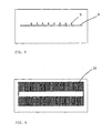
- Fig. 3
- shows a sketch of the sensor point distribution according to a preferred embodiment of the invention.
- Fig. 4
- shows a combined modulation electrode and activation cell for positioning on the sensor chip according to the invention.
- As is evident from the drawings the sensor chip according to the invention preferably consists of a
naked silicon chip 6 in ahousing 7 without a cover (or possibly on a circuit board or ceramic substrate) with a number of layers of metal or another electrically conductive material such as polysilicon, and a dielectric constituting the interface toward the users fingers. The principle is based on imaging sensor elements constituting a part of the third or fourth upper layer of the electrically conductive layers 1 on the silicon circuit, and that the conductor leads, from the elements then is routed individually down to the amplifier circuits on the surface of the silicon chip. - The present solution may be produced industrially by standard methods for ASIC production and packing, as the silicon chip is mounted in a ceramic or plastic based housing without a lid, or on a circuit board or a ceramic substrate. The silicon chip is coupled electrically to the circuit board or housing with so called wire bonding.
- In order to provide the necessary functionality for the capacitance based measuring principle the three or four upper metal layers on the ASIC must be used for different structures with a given electric function as for example illustrated in
fig. 1 . The figure shows a possible solution is not limiting relative to other combinations of layers. - The layers provided on the substrate shown in
figures 1 and 2 shows examples of the construction of an the ASICs upper layers with metal and dielectric, respectively, and will be explained below. The process for realizing the metal and dielectric layers on the silicon chip is well known technology, but the functionality of the individual layers and the combination of these is covered by the present invention, especially aimed at fingerprint sensors, as a variant of the sensor described in international patent applicationWO98/58342 linear sensor array 8, as shown infigure 3 .Figures 2 and3 also show secondary sensor groups which may be used for velocity calculations, as described in the abovementioned patent. A line shaped sensor has the great advantage that it needs far less room and less individual channels than a two dimensional sensor with the same resolution, so that it may be made at a much lower cost. - In
figure 1 the electrical layer 1 constitutes theimaging sensor elements 8. As mentioned the sensor elements may be positioned as shown infigure 3 , as a variant of the patented solution in international patent application NoPCT/N098/00182 - The
dielectric layer 2, infigure 1 , functions as an insulation layer between the conductor leads in the electrically conductive layer 1 and the earth plane in the electricallyconductive layer 3. The layer also constitutes a part of the total dielectric thickness (insulation) between the finger and the sensor element. - The electrically
conductive layer 3 constitutes an earthed plane shielding the conductor leads etc against direct coupling of AC signal from the finger and from themodulation ring 5. Theearthed layer 3 will preferably be shaped so as to cover all conductor leads on the underlying first electrically conductive layer 1, but must have windows over thesensor elements 8. The openings in theearth plane 3 over thesensor elements 8 contributes with a "lens" effect to shape the electric field and thus the capacitive coupling between the finger and the sensor elements, and the shape of thesensor element 8 and the opening in the second electricallyconductive layer 3 may be optimized to maximize the signal strength without going on accord with the geometric resolution of the sensor. - Alternatively the earthed shielding structure may be made using two electrically conductive layers being insulated from each other by a dielectric layer. This will provide an improved shielding and lens effect compared to the use of one layer.
- The second
dielectric layer 4 may insulate between theearth plane 3 and outer electricallyconductive layer 5, and the seconddielectric layer 4 functions as an AC coupling of the signal to the electronics. Thelayer 4 also constitutes (as mentioned above) a part of the total dielectric thickness (insulation) between the finger and thesensor element 8. Since the outer electricallyconductive layer 5 of electrical reasons does not cover the area over thesensor elements 8 the finger will come into contact with the seconddielectric layer 4. Thus this layer must be hard and wear resistant to withstand wear and breakage, as well as chemical influences from the surrounding environment and from the users fingers and other objects. This may be obtained using hard, impenetrable dielectrics such as Si3N4 and SiO2. - The first electrically conductive layer 1 may in some cases be constituted by a coupling between a separate electronic circuit and the first dielectric layer, so that they may be produced separately. These two parts may be produced with so called flip-chip technology.
- In addition the other electrically conductive layers the chip being sketched in
figure 1 comprises a lower electricallyconductive layer 11 making a common earth plane for the circuit. - The outer electrically
conductive layer 5 is the top layer having the purpose of provide a stimulation signal, as mentioned in international patent application NoPCT/NO98/00182 figure 4 . This therefore must be electrically conductive with good coupling to the finger. It must also be hard and wear resistant to withstand wear and breakage, as well as chemical influences from the surroundings and the users fingers. Chrome is a possible metal for this purpose. - Preferably the outer electrical conductive layer is coupled to a drive circuit for controlling frequency and amplitude of the stimulation signal.
- Such an stimulation electrode may be combined with for example a capacitive activation cell being capable of detecting when a finger touches the sensor, and thus be used to control the activation of the sensor from a hibernation mode to active use, to minimize the power consumption of the sensor.
- An impedance activation cell may e.g. be made from as an interdigitated finger structure consisting of two not mutually interconnected "cam structures" (electrodes) 10 being shown in
figure 4 . When a conductive object, e.g. a finger comes close to this structure the impedance between the electrodes will increase, and this change may be detected e.g. by a oscillating circuit operating with low power consumption. - If one of the electrodes is coupled to earth as long as it is in hibernation mode it will provide an effective protection from ESD discharges from a finger or some other charged objects close to the sensor, as the discharge will pass directly to earth. Even if one of these electrodes is not coupled to earth the structures in the outer electrically
conductive layer 10 will have an important function for ESD protection if ESD protecting circuits are coupled between the structures in this layer and earth. - An alternative method for coupling of a stimulation frequency into the finger is to cover the conductive material with a thin dielectric film so that the coupling is made purely capacitive. This may have the advantage that the coupling is more equal from person to person and being independent of the dampness of the finger.
- As the characteristics of the amplifiers and other signal treatment electronics on the chip will vary from element to element, it may be of great importance to be able to calibrate the response from each sensor element. This may be obtained using a transversal electrode close to the line of sensor elements or the conductors leading to them, e.g. as part of the earthed
layer 3 or another electrically conductive layer below it. By providing a calibration signal on this electrode the sensor elements will be excited capacitively without the presence of a finger or other electrically conductive object close to the sensor. Based on the resulting signals from the amplifier and signal treatment electronics it will then be possible to equalize the response from each sensor element. - The present invention consists of a device which in a unique way provides the required advantages for a solid state fingerprint sensor. Corresponding technology may also be used in other applications requiring recognition of finger movements over a surface, e.g. for navigation/mouse purposes.
Claims (8)
- Sensor chip for measuring structures in a finger surface, the sensor chip comprising sensor element forming an essentially linear array and secondary sensor group for velocity calculations in a way known per se, and a silicon chip comprising electronic circuitry, including a number of interrogation electrodes for capacitance measurements, said sensor chip being characterized in that the sensor chip is provided with a first electrically conductive layer, said first electrically conductive layer (1) comprising said sensor elements (8) defining positions of sensors in the sensor chip, said sensor elements (8) being coupled to the interrogation electrodes in the silicon chip (6) and the sensor chip further comprising:a first dielectric layer (2) substantially covering the first electrically conductive layer (1),a second electrically conductive layer (3) comprising openings formed therein over the sensor elements (8), on the first dielectric layer (2) and a second dielectric layer (4) on this, on which an outer electrically conductive layer (5) is mounted, said second electrically conductive layer (3) constituting an earth plane,the outer electrically conductive layer (5) being for electric contact with said structures in said finger surface, and not covering the area over the sensor elements (8),the silicon chip thus being adapted to measure the capacitance between the outer electrically conductive layer (5) and said interrogation electrodes through the sensor elements (8).
- Sensor chip according to claim 1, wherein the first electrically conductive layer (1) is capacitively coupled to the interrogation electrodes.
- Sensor chip according to claim 1, wherein the outer electrically conductive layer (5) is coupled to a drive circuit for controlling the frequency and amplitude of a stimulation signal of the outer electrically conductive layer (5).
- Sensor chip according to claim 1, wherein the second electrically conductive layer (3) constitutes an essentially continuous layer with openings defined over the sensor electrodes in the first electrically conductive layer.
- Sensor chip according to claim 1, wherein the thickness of the two dielectric layers (2, 4) is equal to or less than the distance between the centres of electrical contact points in the first electrically conductive layer (1).
- Sensor chip according to claim 1, comprising a lower electrically conductive layer (11) positioned under the electronic chip.
- Sensor chip according to claim 1, wherein the outer electrically conductive layer (5) is electrically coupled to an electrical modulator in the electronic chip.
- Sensor chip according to claim 1, wherein the outer electrically conductive layer (5) comprises a structure changing impedance, such as a capacitance when coming close to an electrically conductive object, which together with a suitable electrical circuit is adapted to activate the sensor.
Applications Claiming Priority (3)
| Application Number | Priority Date | Filing Date | Title |
|---|---|---|---|
| NO20003003 | 2000-06-09 | ||
| NO20003003A NO315016B1 (en) | 2000-06-09 | 2000-06-09 | Miniature sensor |
| PCT/NO2001/000239 WO2001099036A2 (en) | 2000-06-09 | 2001-06-08 | Miniature sensor chip, especially for fingerprint sensors |
Publications (2)
| Publication Number | Publication Date |
|---|---|
| EP1303829A2 EP1303829A2 (en) | 2003-04-23 |
| EP1303829B1 true EP1303829B1 (en) | 2008-08-13 |
Family
ID=19911249
Family Applications (1)
| Application Number | Title | Priority Date | Filing Date |
|---|---|---|---|
| EP01938854A Expired - Lifetime EP1303829B1 (en) | 2000-06-09 | 2001-06-08 | Miniature sensor chip, especially for fingerprint sensors |
Country Status (10)
| Country | Link |
|---|---|
| US (2) | US7283651B2 (en) |
| EP (1) | EP1303829B1 (en) |
| JP (1) | JP4818564B2 (en) |
| AT (1) | ATE404934T1 (en) |
| AU (1) | AU2001264430A1 (en) |
| DE (1) | DE60135346D1 (en) |
| DK (1) | DK1303829T3 (en) |
| ES (1) | ES2312443T3 (en) |
| NO (1) | NO315016B1 (en) |
| WO (1) | WO2001099036A2 (en) |
Families Citing this family (29)
| Publication number | Priority date | Publication date | Assignee | Title |
|---|---|---|---|---|
| NO315016B1 (en) * | 2000-06-09 | 2003-06-23 | Idex Asa | Miniature sensor |
| NO315017B1 (en) * | 2000-06-09 | 2003-06-23 | Idex Asa | Sensor chip, especially for measuring structures in a finger surface |
| ATE336753T1 (en) | 2001-12-07 | 2006-09-15 | Idex Asa | SENSOR FOR WET AND DRY FINGERS MEASUREMENTS |
| NO316796B1 (en) * | 2002-03-01 | 2004-05-10 | Idex Asa | Sensor module for painting structures in a surface, especially a finger surface |
| FI115109B (en) | 2003-01-22 | 2005-02-28 | Nokia Corp | Sensor arrangement and mobile communicator comprising a sensor arrangement |
| FI20030102A0 (en) | 2003-01-22 | 2003-01-22 | Nokia Corp | Device for verification of a person |
| US7474772B2 (en) | 2003-06-25 | 2009-01-06 | Atrua Technologies, Inc. | System and method for a miniature user input device |
| US7587072B2 (en) | 2003-08-22 | 2009-09-08 | Authentec, Inc. | System for and method of generating rotational inputs |
| FI121352B (en) * | 2003-12-18 | 2010-10-15 | Upm Kymmene Corp | Radio frequency technology based sensor arrangement and method |
| US7697729B2 (en) | 2004-01-29 | 2010-04-13 | Authentec, Inc. | System for and method of finger initiated actions |
| US8131026B2 (en) | 2004-04-16 | 2012-03-06 | Validity Sensors, Inc. | Method and apparatus for fingerprint image reconstruction |
| US8447077B2 (en) * | 2006-09-11 | 2013-05-21 | Validity Sensors, Inc. | Method and apparatus for fingerprint motion tracking using an in-line array |
| DE602005022900D1 (en) | 2004-10-04 | 2010-09-23 | Validity Sensors Inc | FINGERPRINTER CONSTRUCTIONS WITH ONE SUBSTRATE |
| US7831070B1 (en) | 2005-02-18 | 2010-11-09 | Authentec, Inc. | Dynamic finger detection mechanism for a fingerprint sensor |
| US8231056B2 (en) | 2005-04-08 | 2012-07-31 | Authentec, Inc. | System for and method of protecting an integrated circuit from over currents |
| JP4943807B2 (en) * | 2006-10-18 | 2012-05-30 | 日本電信電話株式会社 | Impedance detection device, impedance detection method, biometric recognition device, and fingerprint authentication device |
| NO20093601A1 (en) * | 2009-12-29 | 2011-06-30 | Idex Asa | surface Sensor |
| US8421890B2 (en) | 2010-01-15 | 2013-04-16 | Picofield Technologies, Inc. | Electronic imager using an impedance sensor grid array and method of making |
| US8791792B2 (en) | 2010-01-15 | 2014-07-29 | Idex Asa | Electronic imager using an impedance sensor grid array mounted on or about a switch and method of making |
| US8866347B2 (en) | 2010-01-15 | 2014-10-21 | Idex Asa | Biometric image sensing |
| US9437478B2 (en) * | 2010-05-11 | 2016-09-06 | Xintec Inc. | Chip package and method for forming the same |
| US9425134B2 (en) | 2010-05-11 | 2016-08-23 | Xintec Inc. | Chip package |
| WO2013155224A1 (en) | 2012-04-10 | 2013-10-17 | Picofield Technologies Inc. | Biometric sensing |
| NO20131423A1 (en) | 2013-02-22 | 2014-08-25 | Idex Asa | Integrated fingerprint sensor |
| US10095906B2 (en) | 2014-02-21 | 2018-10-09 | Idex Asa | Sensor employing overlapping grid lines and conductive probes for extending a sensing surface from the grid lines |
| US9779280B2 (en) | 2014-12-24 | 2017-10-03 | Idex Asa | Fingerprint sensor employing an integrated noise rejection structure |
| US10613243B2 (en) * | 2017-04-27 | 2020-04-07 | Franklin Sensors Inc. | Apparatus and methods for obscured feature detection |
| US10895657B2 (en) * | 2017-01-13 | 2021-01-19 | Franklin Sensors Inc. | Apparatus and methods for obscured feature detection with uniform electric fields |
| WO2018169107A1 (en) * | 2017-03-17 | 2018-09-20 | 전용원 | Fingerprint recognition sensor and system for improving sensing offset |
Citations (1)
| Publication number | Priority date | Publication date | Assignee | Title |
|---|---|---|---|---|
| WO1998058342A1 (en) * | 1997-06-16 | 1998-12-23 | Sintef | Method and apparatus for measuring structures in a fingerprint |
Family Cites Families (21)
| Publication number | Priority date | Publication date | Assignee | Title |
|---|---|---|---|---|
| US5399898A (en) * | 1992-07-17 | 1995-03-21 | Lsi Logic Corporation | Multi-chip semiconductor arrangements using flip chip dies |
| US5371404A (en) * | 1993-02-04 | 1994-12-06 | Motorola, Inc. | Thermally conductive integrated circuit package with radio frequency shielding |
| TW303441B (en) * | 1995-03-29 | 1997-04-21 | Trw Inc | |
| US6049620A (en) * | 1995-12-15 | 2000-04-11 | Veridicom, Inc. | Capacitive fingerprint sensor with adjustable gain |
| US5963679A (en) * | 1996-01-26 | 1999-10-05 | Harris Corporation | Electric field fingerprint sensor apparatus and related methods |
| JP4024335B2 (en) * | 1996-01-26 | 2007-12-19 | ハリス コーポレイション | Integrated circuit device having an opening exposing die of integrated circuit and manufacturing method thereof |
| US5956415A (en) * | 1996-01-26 | 1999-09-21 | Harris Corporation | Enhanced security fingerprint sensor package and related methods |
| US6020749A (en) * | 1996-11-12 | 2000-02-01 | Hewlett-Packard Company | Method and apparatus for performing testing of double-sided ball grid array devices |
| US5920640A (en) * | 1997-05-16 | 1999-07-06 | Harris Corporation | Fingerprint sensor and token reader and associated methods |
| US5940526A (en) * | 1997-05-16 | 1999-08-17 | Harris Corporation | Electric field fingerprint sensor having enhanced features and related methods |
| US6259804B1 (en) * | 1997-05-16 | 2001-07-10 | Authentic, Inc. | Fingerprint sensor with gain control features and associated methods |
| JP3592487B2 (en) * | 1997-07-02 | 2004-11-24 | 日本電信電話株式会社 | Fingerprint recognition integrated circuit |
| US6483931B2 (en) * | 1997-09-11 | 2002-11-19 | Stmicroelectronics, Inc. | Electrostatic discharge protection of a capacitve type fingerprint sensing array |
| JP3102395B2 (en) * | 1997-11-27 | 2000-10-23 | 日本電気株式会社 | Fingerprint detection device |
| NO307065B1 (en) * | 1998-02-26 | 2000-01-31 | Idex As | fingerprint Sensor |
| EP0941696A1 (en) * | 1998-03-03 | 1999-09-15 | Siemens Aktiengesellschaft | Fingertipsensor with integrated bushbutton switch |
| US6026564A (en) * | 1998-04-10 | 2000-02-22 | Ang Technologies Inc. | Method of making a high density multilayer wiring board |
| US7184581B2 (en) * | 2000-06-09 | 2007-02-27 | Idex Asa | System for real time finger surface pattern measurement |
| NO315017B1 (en) * | 2000-06-09 | 2003-06-23 | Idex Asa | Sensor chip, especially for measuring structures in a finger surface |
| NO315016B1 (en) * | 2000-06-09 | 2003-06-23 | Idex Asa | Miniature sensor |
| NO316796B1 (en) * | 2002-03-01 | 2004-05-10 | Idex Asa | Sensor module for painting structures in a surface, especially a finger surface |
-
2000
- 2000-06-09 NO NO20003003A patent/NO315016B1/en not_active IP Right Cessation
-
2001
- 2001-06-08 JP JP2002503804A patent/JP4818564B2/en not_active Expired - Fee Related
- 2001-06-08 EP EP01938854A patent/EP1303829B1/en not_active Expired - Lifetime
- 2001-06-08 DK DK01938854T patent/DK1303829T3/en active
- 2001-06-08 WO PCT/NO2001/000239 patent/WO2001099036A2/en not_active Ceased
- 2001-06-08 AT AT01938854T patent/ATE404934T1/en active
- 2001-06-08 DE DE60135346T patent/DE60135346D1/en not_active Expired - Lifetime
- 2001-06-08 ES ES01938854T patent/ES2312443T3/en not_active Expired - Lifetime
- 2001-06-08 AU AU2001264430A patent/AU2001264430A1/en not_active Abandoned
- 2001-06-08 US US10/297,745 patent/US7283651B2/en not_active Expired - Fee Related
-
2007
- 2007-08-13 US US11/837,760 patent/US7518382B2/en not_active Expired - Lifetime
Patent Citations (1)
| Publication number | Priority date | Publication date | Assignee | Title |
|---|---|---|---|---|
| WO1998058342A1 (en) * | 1997-06-16 | 1998-12-23 | Sintef | Method and apparatus for measuring structures in a fingerprint |
Also Published As
| Publication number | Publication date |
|---|---|
| US7518382B2 (en) | 2009-04-14 |
| DK1303829T3 (en) | 2008-12-15 |
| US20030161511A1 (en) | 2003-08-28 |
| NO20003003D0 (en) | 2000-06-09 |
| US7283651B2 (en) | 2007-10-16 |
| AU2001264430A1 (en) | 2002-01-02 |
| NO20003003L (en) | 2001-12-10 |
| EP1303829A2 (en) | 2003-04-23 |
| WO2001099036A3 (en) | 2002-04-25 |
| JP4818564B2 (en) | 2011-11-16 |
| NO315016B1 (en) | 2003-06-23 |
| JP2003535668A (en) | 2003-12-02 |
| ATE404934T1 (en) | 2008-08-15 |
| WO2001099036A2 (en) | 2001-12-27 |
| DE60135346D1 (en) | 2008-09-25 |
| ES2312443T3 (en) | 2009-03-01 |
| US20080030207A1 (en) | 2008-02-07 |
Similar Documents
| Publication | Publication Date | Title |
|---|---|---|
| US7518382B2 (en) | Miniature sensor chip, especially for finger print sensors | |
| EP1303828B1 (en) | Sensor Unit, especially for Fingerprint Sensors | |
| US8487624B2 (en) | Surface sensor | |
| EP1581111B1 (en) | Sensor module for measuring surfaces | |
| KR100751069B1 (en) | Improved sensing arrangement | |
| WO2004008161A1 (en) | Capacitive two dimensional sensor | |
| KR20160032132A (en) | Surface sensor | |
| JP7439920B2 (en) | sensor device | |
| NO318882B1 (en) | Substrate multiplexing |
Legal Events
| Date | Code | Title | Description |
|---|---|---|---|
| PUAI | Public reference made under article 153(3) epc to a published international application that has entered the european phase |
Free format text: ORIGINAL CODE: 0009012 |
|
| 17P | Request for examination filed |
Effective date: 20030108 |
|
| AK | Designated contracting states |
Designated state(s): AT BE CH CY DE DK ES FI FR GB GR IE IT LI LU MC NL PT SE TR |
|
| AX | Request for extension of the european patent |
Extension state: AL LT LV MK RO SI |
|
| RIN1 | Information on inventor provided before grant (corrected) |
Inventor name: TSCHUDI, JON Inventor name: NYSAETHER, JON Inventor name: JOHANSEN, IB-RUNE Inventor name: VERMESAN, OVIDIU |
|
| RAP1 | Party data changed (applicant data changed or rights of an application transferred) |
Owner name: IDEX ASA |
|
| RIN1 | Information on inventor provided before grant (corrected) |
Inventor name: TSCHUDI, JON Inventor name: VERMESAN, OVIDIU Inventor name: NYSAETHER, JON Inventor name: JOHANSEN, IB-RUNE |
|
| 17Q | First examination report despatched |
Effective date: 20061219 |
|
| RAP1 | Party data changed (applicant data changed or rights of an application transferred) |
Owner name: IDEX ASA |
|
| GRAP | Despatch of communication of intention to grant a patent |
Free format text: ORIGINAL CODE: EPIDOSNIGR1 |
|
| GRAS | Grant fee paid |
Free format text: ORIGINAL CODE: EPIDOSNIGR3 |
|
| GRAA | (expected) grant |
Free format text: ORIGINAL CODE: 0009210 |
|
| AK | Designated contracting states |
Kind code of ref document: B1 Designated state(s): AT BE CH CY DE DK ES FI FR GB GR IE IT LI LU MC NL PT SE TR |
|
| AX | Request for extension of the european patent |
Extension state: AL LT LV MK RO SI |
|
| REG | Reference to a national code |
Ref country code: GB Ref legal event code: FG4D |
|
| REG | Reference to a national code |
Ref country code: CH Ref legal event code: EP |
|
| REG | Reference to a national code |
Ref country code: IE Ref legal event code: FG4D |
|
| REF | Corresponds to: |
Ref document number: 60135346 Country of ref document: DE Date of ref document: 20080925 Kind code of ref document: P |
|
| REG | Reference to a national code |
Ref country code: SE Ref legal event code: TRGR |
|
| REG | Reference to a national code |
Ref country code: CH Ref legal event code: NV Representative=s name: DR. GRAF & PARTNER INTELLECTUAL PROPERTY |
|
| REG | Reference to a national code |
Ref country code: DK Ref legal event code: T3 |
|
| LTIE | Lt: invalidation of european patent or patent extension |
Effective date: 20080813 |
|
| REG | Reference to a national code |
Ref country code: ES Ref legal event code: FG2A Ref document number: 2312443 Country of ref document: ES Kind code of ref document: T3 |
|
| PG25 | Lapsed in a contracting state [announced via postgrant information from national office to epo] |
Ref country code: PT Free format text: LAPSE BECAUSE OF FAILURE TO SUBMIT A TRANSLATION OF THE DESCRIPTION OR TO PAY THE FEE WITHIN THE PRESCRIBED TIME-LIMIT Effective date: 20090113 |
|
| PLBE | No opposition filed within time limit |
Free format text: ORIGINAL CODE: 0009261 |
|
| STAA | Information on the status of an ep patent application or granted ep patent |
Free format text: STATUS: NO OPPOSITION FILED WITHIN TIME LIMIT |
|
| 26N | No opposition filed |
Effective date: 20090514 |
|
| PG25 | Lapsed in a contracting state [announced via postgrant information from national office to epo] |
Ref country code: MC Free format text: LAPSE BECAUSE OF NON-PAYMENT OF DUE FEES Effective date: 20090630 |
|
| REG | Reference to a national code |
Ref country code: CH Ref legal event code: PFA Owner name: IDEX ASA Free format text: IDEX ASA#SNAROYVEIEN 30#1330 FORNEBU (NO) -TRANSFER TO- IDEX ASA#SNAROYVEIEN 30#1330 FORNEBU (NO) |
|
| PG25 | Lapsed in a contracting state [announced via postgrant information from national office to epo] |
Ref country code: GR Free format text: LAPSE BECAUSE OF FAILURE TO SUBMIT A TRANSLATION OF THE DESCRIPTION OR TO PAY THE FEE WITHIN THE PRESCRIBED TIME-LIMIT Effective date: 20081114 |
|
| PG25 | Lapsed in a contracting state [announced via postgrant information from national office to epo] |
Ref country code: LU Free format text: LAPSE BECAUSE OF NON-PAYMENT OF DUE FEES Effective date: 20090608 |
|
| PG25 | Lapsed in a contracting state [announced via postgrant information from national office to epo] |
Ref country code: TR Free format text: LAPSE BECAUSE OF FAILURE TO SUBMIT A TRANSLATION OF THE DESCRIPTION OR TO PAY THE FEE WITHIN THE PRESCRIBED TIME-LIMIT Effective date: 20080813 |
|
| PG25 | Lapsed in a contracting state [announced via postgrant information from national office to epo] |
Ref country code: CY Free format text: LAPSE BECAUSE OF FAILURE TO SUBMIT A TRANSLATION OF THE DESCRIPTION OR TO PAY THE FEE WITHIN THE PRESCRIBED TIME-LIMIT Effective date: 20080813 |
|
| PGFP | Annual fee paid to national office [announced via postgrant information from national office to epo] |
Ref country code: IE Payment date: 20140624 Year of fee payment: 14 |
|
| PGFP | Annual fee paid to national office [announced via postgrant information from national office to epo] |
Ref country code: CH Payment date: 20140617 Year of fee payment: 14 Ref country code: FI Payment date: 20140617 Year of fee payment: 14 Ref country code: AT Payment date: 20140702 Year of fee payment: 14 |
|
| PGFP | Annual fee paid to national office [announced via postgrant information from national office to epo] |
Ref country code: DK Payment date: 20140625 Year of fee payment: 14 |
|
| PGFP | Annual fee paid to national office [announced via postgrant information from national office to epo] |
Ref country code: BE Payment date: 20140624 Year of fee payment: 14 |
|
| PGFP | Annual fee paid to national office [announced via postgrant information from national office to epo] |
Ref country code: ES Payment date: 20140704 Year of fee payment: 14 |
|
| PGFP | Annual fee paid to national office [announced via postgrant information from national office to epo] |
Ref country code: IT Payment date: 20140630 Year of fee payment: 14 |
|
| REG | Reference to a national code |
Ref country code: DK Ref legal event code: EBP Effective date: 20150630 |
|
| PG25 | Lapsed in a contracting state [announced via postgrant information from national office to epo] |
Ref country code: FI Free format text: LAPSE BECAUSE OF NON-PAYMENT OF DUE FEES Effective date: 20150608 Ref country code: IT Free format text: LAPSE BECAUSE OF NON-PAYMENT OF DUE FEES Effective date: 20150608 |
|
| REG | Reference to a national code |
Ref country code: CH Ref legal event code: PL |
|
| REG | Reference to a national code |
Ref country code: AT Ref legal event code: MM01 Ref document number: 404934 Country of ref document: AT Kind code of ref document: T Effective date: 20150608 |
|
| REG | Reference to a national code |
Ref country code: IE Ref legal event code: MM4A |
|
| PG25 | Lapsed in a contracting state [announced via postgrant information from national office to epo] |
Ref country code: LI Free format text: LAPSE BECAUSE OF NON-PAYMENT OF DUE FEES Effective date: 20150630 Ref country code: CH Free format text: LAPSE BECAUSE OF NON-PAYMENT OF DUE FEES Effective date: 20150630 Ref country code: IE Free format text: LAPSE BECAUSE OF NON-PAYMENT OF DUE FEES Effective date: 20150608 |
|
| REG | Reference to a national code |
Ref country code: FR Ref legal event code: PLFP Year of fee payment: 16 |
|
| PG25 | Lapsed in a contracting state [announced via postgrant information from national office to epo] |
Ref country code: AT Free format text: LAPSE BECAUSE OF NON-PAYMENT OF DUE FEES Effective date: 20150608 |
|
| REG | Reference to a national code |
Ref country code: ES Ref legal event code: FD2A Effective date: 20160728 |
|
| PG25 | Lapsed in a contracting state [announced via postgrant information from national office to epo] |
Ref country code: DK Free format text: LAPSE BECAUSE OF NON-PAYMENT OF DUE FEES Effective date: 20150630 |
|
| PG25 | Lapsed in a contracting state [announced via postgrant information from national office to epo] |
Ref country code: ES Free format text: LAPSE BECAUSE OF NON-PAYMENT OF DUE FEES Effective date: 20150609 |
|
| REG | Reference to a national code |
Ref country code: FR Ref legal event code: PLFP Year of fee payment: 17 |
|
| PG25 | Lapsed in a contracting state [announced via postgrant information from national office to epo] |
Ref country code: BE Free format text: LAPSE BECAUSE OF NON-PAYMENT OF DUE FEES Effective date: 20150630 |
|
| REG | Reference to a national code |
Ref country code: FR Ref legal event code: PLFP Year of fee payment: 18 |
|
| PGFP | Annual fee paid to national office [announced via postgrant information from national office to epo] |
Ref country code: NL Payment date: 20180613 Year of fee payment: 18 Ref country code: DE Payment date: 20180530 Year of fee payment: 18 |
|
| PGFP | Annual fee paid to national office [announced via postgrant information from national office to epo] |
Ref country code: FR Payment date: 20180524 Year of fee payment: 18 |
|
| PGFP | Annual fee paid to national office [announced via postgrant information from national office to epo] |
Ref country code: SE Payment date: 20180612 Year of fee payment: 18 |
|
| PGFP | Annual fee paid to national office [announced via postgrant information from national office to epo] |
Ref country code: GB Payment date: 20180606 Year of fee payment: 18 |
|
| REG | Reference to a national code |
Ref country code: DE Ref legal event code: R119 Ref document number: 60135346 Country of ref document: DE |
|
| REG | Reference to a national code |
Ref country code: SE Ref legal event code: EUG |
|
| PG25 | Lapsed in a contracting state [announced via postgrant information from national office to epo] |
Ref country code: SE Free format text: LAPSE BECAUSE OF NON-PAYMENT OF DUE FEES Effective date: 20190609 |
|
| REG | Reference to a national code |
Ref country code: NL Ref legal event code: MM Effective date: 20190701 |
|
| GBPC | Gb: european patent ceased through non-payment of renewal fee |
Effective date: 20190608 |
|
| PG25 | Lapsed in a contracting state [announced via postgrant information from national office to epo] |
Ref country code: GB Free format text: LAPSE BECAUSE OF NON-PAYMENT OF DUE FEES Effective date: 20190608 Ref country code: DE Free format text: LAPSE BECAUSE OF NON-PAYMENT OF DUE FEES Effective date: 20200101 Ref country code: NL Free format text: LAPSE BECAUSE OF NON-PAYMENT OF DUE FEES Effective date: 20190701 |
|
| PG25 | Lapsed in a contracting state [announced via postgrant information from national office to epo] |
Ref country code: FR Free format text: LAPSE BECAUSE OF NON-PAYMENT OF DUE FEES Effective date: 20190630 |