EP1303011A1 - Electrical connector with reduced crosstalk - Google Patents
Electrical connector with reduced crosstalk Download PDFInfo
- Publication number
- EP1303011A1 EP1303011A1 EP02022112A EP02022112A EP1303011A1 EP 1303011 A1 EP1303011 A1 EP 1303011A1 EP 02022112 A EP02022112 A EP 02022112A EP 02022112 A EP02022112 A EP 02022112A EP 1303011 A1 EP1303011 A1 EP 1303011A1
- Authority
- EP
- European Patent Office
- Prior art keywords
- contacts
- ground
- connector
- contact
- pair
- Prior art date
- Legal status (The legal status is an assumption and is not a legal conclusion. Google has not performed a legal analysis and makes no representation as to the accuracy of the status listed.)
- Granted
Links
Images









Classifications
-
- H—ELECTRICITY
- H01—ELECTRIC ELEMENTS
- H01R—ELECTRICALLY-CONDUCTIVE CONNECTIONS; STRUCTURAL ASSOCIATIONS OF A PLURALITY OF MUTUALLY-INSULATED ELECTRICAL CONNECTING ELEMENTS; COUPLING DEVICES; CURRENT COLLECTORS
- H01R13/00—Details of coupling devices of the kinds covered by groups H01R12/70 or H01R24/00 - H01R33/00
- H01R13/646—Details of coupling devices of the kinds covered by groups H01R12/70 or H01R24/00 - H01R33/00 specially adapted for high-frequency, e.g. structures providing an impedance match or phase match
- H01R13/6473—Impedance matching
-
- H—ELECTRICITY
- H01—ELECTRIC ELEMENTS
- H01R—ELECTRICALLY-CONDUCTIVE CONNECTIONS; STRUCTURAL ASSOCIATIONS OF A PLURALITY OF MUTUALLY-INSULATED ELECTRICAL CONNECTING ELEMENTS; COUPLING DEVICES; CURRENT COLLECTORS
- H01R13/00—Details of coupling devices of the kinds covered by groups H01R12/70 or H01R24/00 - H01R33/00
- H01R13/648—Protective earth or shield arrangements on coupling devices, e.g. anti-static shielding
- H01R13/658—High frequency shielding arrangements, e.g. against EMI [Electro-Magnetic Interference] or EMP [Electro-Magnetic Pulse]
- H01R13/6591—Specific features or arrangements of connection of shield to conductive members
- H01R13/6592—Specific features or arrangements of connection of shield to conductive members the conductive member being a shielded cable
-
- H—ELECTRICITY
- H01—ELECTRIC ELEMENTS
- H01R—ELECTRICALLY-CONDUCTIVE CONNECTIONS; STRUCTURAL ASSOCIATIONS OF A PLURALITY OF MUTUALLY-INSULATED ELECTRICAL CONNECTING ELEMENTS; COUPLING DEVICES; CURRENT COLLECTORS
- H01R13/00—Details of coupling devices of the kinds covered by groups H01R12/70 or H01R24/00 - H01R33/00
- H01R13/646—Details of coupling devices of the kinds covered by groups H01R12/70 or H01R24/00 - H01R33/00 specially adapted for high-frequency, e.g. structures providing an impedance match or phase match
- H01R13/6461—Means for preventing cross-talk
- H01R13/6471—Means for preventing cross-talk by special arrangement of ground and signal conductors, e.g. GSGS [Ground-Signal-Ground-Signal]
-
- H—ELECTRICITY
- H01—ELECTRIC ELEMENTS
- H01R—ELECTRICALLY-CONDUCTIVE CONNECTIONS; STRUCTURAL ASSOCIATIONS OF A PLURALITY OF MUTUALLY-INSULATED ELECTRICAL CONNECTING ELEMENTS; COUPLING DEVICES; CURRENT COLLECTORS
- H01R13/00—Details of coupling devices of the kinds covered by groups H01R12/70 or H01R24/00 - H01R33/00
- H01R13/648—Protective earth or shield arrangements on coupling devices, e.g. anti-static shielding
- H01R13/658—High frequency shielding arrangements, e.g. against EMI [Electro-Magnetic Interference] or EMP [Electro-Magnetic Pulse]
- H01R13/6581—Shield structure
-
- H—ELECTRICITY
- H01—ELECTRIC ELEMENTS
- H01R—ELECTRICALLY-CONDUCTIVE CONNECTIONS; STRUCTURAL ASSOCIATIONS OF A PLURALITY OF MUTUALLY-INSULATED ELECTRICAL CONNECTING ELEMENTS; COUPLING DEVICES; CURRENT COLLECTORS
- H01R13/00—Details of coupling devices of the kinds covered by groups H01R12/70 or H01R24/00 - H01R33/00
- H01R13/648—Protective earth or shield arrangements on coupling devices, e.g. anti-static shielding
- H01R13/658—High frequency shielding arrangements, e.g. against EMI [Electro-Magnetic Interference] or EMP [Electro-Magnetic Pulse]
- H01R13/6581—Shield structure
- H01R13/6585—Shielding material individually surrounding or interposed between mutually spaced contacts
- H01R13/6589—Shielding material individually surrounding or interposed between mutually spaced contacts with wires separated by conductive housing parts
Definitions
- This invention relates to an electrical connector, which will simply be referred to as "connector”, and in particular, to a connector for use in a high-speed signal transmission system.
- a connector for the high-speed signaling or the differential signaling
- a connector has a pair of contacts for receiving/transmitting a pair of signals opposite in voltage, that is, a pair of positive and negative voltage signals.
- the differential signaling is often used in the high-speed transmission system in order to achieve excellent noise immunity.
- the paired contacts will be called a "differential pair of contacts”.
- the paired signals will be called a "differential pair of signals”.
- a differential pair of signals are transmitted through a pair of signal lines, for example, a pair of coaxial cables, twin (parallel) coaxial cable, or a twin (twisted) axial cable (Twinax cable), from or to a connector.
- a pair of center conductors which are center conductors of the pair of coaxial cables (namely, a pair of positive and negative signal lines), are connected to the differential pair of contacts in the connector.
- a pair of outer conductors of the pair of coaxial cables are bundled and are connected to a ground contact in the connector.
- twin coaxial cable In the case of using a twin (parallel) coaxial cable, the pair of inner conductors of the twin coaxial cable are connected to differential pair of contacts in the connector, while an outer conductor of the twin coaxial cable is connected to a ground contact in the connector.
- twinax cable In use of the twinax cable, twisted twin conductors are connected to the differential pair of contacts, respectively, while a drain line is connected to the ground contact.
- a connector usually comprises a plurality of contacts arranged in rows of contacts and each row may include two differential pairs of contacts.
- a single ground contact is generally arranged between two differential pairs of contacts, in order to minimize interference between two differential pairs of signals passing through the two differential pairs of contacts and to minimize the number of contacts in a connector. That is, a differential pair of contacts, a ground contact and another differential pair of contacts are arranged in that order so that the ground contact is shared by the different pairs of contacts.
- pin (contact) assignments there is an existing connector compliant to the physical interconnect specification of the DVI (Digital Video Interface) made by the DDWG (Digital Display Working Group whose URL is "http://www.ddwg.org/").
- a connector compliant to the DVI specification supports Transmission Minimized Differential Signaling (TMDS) so that a differential pair of contacts receive/transmit a pair of positive and negative signals, that is, a differential pair of signals, under the TMDS.
- TMDS Transmission Minimized Differential Signaling
- the present inventors point out here that the above-mentioned pin assignments are non-symmetric ones and that one contact of a differential pair of contacts is farther than the other of the differential pair of contacts from a corresponding ground contact.
- an imbalance on impedance might arise from the non-symmetric pin assignments and, if arising, it makes electrical path lengths of a differential pair of positive and negative signals different from each other because the physical path lengths of the differential pair of signals are usually the same. If there is a large difference in electrical path lengths of a differential pair of signals, a critical difference occurs between transmission delays of the differential pair of signals so that the differential pair of signals do not suitably work any longer. Therefore, an impedance imbalance arising from the non-symmetric pin assignments should be compensated.
- an output impedance of a connector, especially, on every contact is normally predefined in order to make an impedance matching between it and an input impedance of a mating connector on every contact. This requirement has to be met on compensating the imbalance mentioned above.
- a connector for connecting at least first and second signal lines and a ground line with a mating connector fitable to said connector, said connector comprising a ground plate (1), an insulator (30), first and second contacts (21) being to be connected with said first and second signal lines, respectively, and a ground contact (22) being to be connected with said ground line, said ground plate (1) being electrically connected with said ground contact (22), said insulator (30) supporting therein said first and second contacts (21) and said ground contact (22) in accordance with predetermined pin assignments where said first and second contacts (21) and said ground contact (22) are arranged in the same row so that said first contact (21, 108) is positioned farther than said second contact (21, 108) from said ground contact (22, 106), said connector being characterized by provision of a conductive finger portion (3) disposed in the proximity of said first contact (21, 108), said conductive finger portion (3) being electrically connected with said ground plate (1).
- said insulator (30) has first to third through holes (35) and an additional hole (34), said first to third through holes (35) being arranged in the same horizontal line so as to receive said first and second contacts (21), and said ground contact (22) inserted thereinto, respectively, in accordance with said predetermined pin assignments, said additional hole (34) accommodating therein said conductive finger portion (3) and being located above or below said first through hole (35) in the insulator (30).
- a connector according to an embodiment of the present invention is used in a system for transmitting high-frequency signals between a personal computer and its monitor.
- the connector 10 comprises a plurality of contacts 21, 22, and 24, an insulator housing 30 supporting therein the contacts 21, 22 and 24, a shell 11 surrounding the contacts 21, 22 and 24 and the insulator housing 30, and ground plates 1 (1a, 1b, 1c).
- the front end of the connector 10 in a Z-direction is formed with a fitting portion for a mating connector, which is not shown. That is, the Z-direction is an insertion direction of the connector for the mating connector.
- cables carrying the high-speed signals are fixed on the rear side of the connector 10 in the Z-direction. The installation of the cables is described later with reference to further drawings.
- a key 23 is provided, as a positioning means on the insertion for the mating connector, in the fitting portion of the front side in the Z-direction.
- the key 23 may be omitted, depending on the strength of the shell 11, the contacts 21, 22, 24 and so on.
- the connector 10 has twenty-four contacts 21, 22, 24.
- the contacts depicted with the reference numeral 21 are signal contacts for receiving or transmitting the differential pair of signals in the high-speed signal transmission system. That is, two adjacent contacts 21 form a differential pair of contacts.
- the contacts depicted with the reference numeral 22 are ground contacts and are connected to corresponding ones of the ground plates 1, respectively.
- the contacts depicted with the reference numeral 24 are contacts which are used for a particular purpose other than high-speed signal transmission and a ground thereof.
- a Y-direction is from the bottom to the top of the connector 10
- an X-direction is from the left side to the right side of the connector 10 as seen from the front side of the connector 10.
- a unique reference numeral is also assigned to every contact in Fig. 10, the unique reference numeral of each contact being shown in the parentheses corresponding to the contact.
- the contacts 21, 22, 24 are arranged in three rows, namely, a top row, a middle row, and a bottom row, each of which comprises eight contacts 101 to 108, 109 to 116, and 117 to 124. In other words, those contacts are arranged in eight columns each column including three contacts.
- the top row comprises three contacts 24 (101 to 103), four signal contacts 21 (104, 105, 107, 108) and one ground contact 22 (106).
- the two adjacent ones of signal contacts 21 (104, 105) are a differential pair of contacts, while the other two adjacent ones of the signal contacts 21 (107, 108) are another differential pair of contacts.
- the middle row comprises three contacts 24 (109 to 111), four signal contacts 21 (112, 113, 115, 116) and one ground contact 22 (114). Among them, two adjacent ones of the signal contacts 21 (112, 113) are a differential pair of contacts, while the other two adjacent signal contacts 21 (115, 116) are another differential pair of contacts. These two differential pairs of contacts 21 (112, 113, 115, 116) share the ground contact 22 (114) disposed therebetween.
- the bottom row comprises six signal contacts 21 (117, 118, 120, 121, 123, 124) and two ground contacts 22 (119, 122).
- two adjacent ones of the signal contacts 21 are a differential pair of contacts and one of the ground contacts 22 (119) corresponds to the differential pair of contacts.
- another two adjacent ones of the signal contacts 21 120, 121) are another differential pair of contacts, while the other two adjacent ones of the signal contacts 21 (123, 124) are yet another pair of contacts.
- These two differential pairs of contacts 21 120, 121, 123, 124) share the other one of ground contact 22 (122) disposed therebetween.
- the connector 10 further comprises seven conductive finger portions, conductive tab portion, or thin or narrow conductive members 3, which are shown by broken lines in Fig. 10. Every conductive finger portion 3 is electrically connected through the ground plates 1 to the ground contacts 22 (106, 114, 118, 122). In addition, each conductive finger portion 3 is arranged in the proximity of the signal contact 21 (104, 108, 112, 116, 117, 120, 124) which is positioned farther than the other signal contact 21 (105, 107, 113, 115, 118, 121, 123) from the ground contact 22 (106, 114, 119, 122) in each of the differential pairs of contacts.
- each of the illustrated conductive finger portions 3 is located below the corresponding signal contact 21 (104, 108, 112, 116, 117, 120, 124), but may be located above thereof.
- the conductive finger portions 3 compensate the impedance imbalance arising from the pin assignments of the signal contacts 21 mentioned above, by adjusting the impedance of the signal contacts (104, 108, 112, 116, 117, 120, 124) to the substantially same level as that of the respective the other signal contacts (105, 107, 113, 115, 118, 121, 123).
- the shell 11 comprises a front tubular portion 13 for being fitted with the mating connector installed for example on a board of an electronic device not shown, a rear tubular portion 14 having a shape of a rectangular tube, and two flange portions 12 outwardly projecting opposite to each other in the X-direction from a joint portion between the front tubular portion 13 and the rear tubular portion 14.
- the flange portions 12 have circular holes 12a for screws used for fixing and ensuring the connection between the connector 10 and the mating connector.
- the front tubular portion 13 has dimples 13a in its top and bottom outer surfaces, which serve to insure the electrical connection between the shell 11 of the connector 10 and a shell of the mating connector.
- the rear tubular portion 14 is provided with edge portions 14a, 14a, 14b, 14b on the top, the bottom, and the opposite sides at the end portion thereof, those edge portions being bent toward the inside and then slightly divergent rearwardly.
- the rear tubular portion 14 is also provided with five openings 14c in the top and the bottom walls thereof.
- the rear tubular portion 14 is provided with hook portions 14c1 in the top and the bottom walls by making five U-shaped incisions or lance slits in the top and the bottom walls (e.g. see Fig. 12).
- the hook portions 14c1 are bent toward the insulator housing installed in the rear tubular portion 14, so that the openings 14c are formed in the top and bottom walls of the rear tubular portion 14 as mentioned above. Resultantly, the bent hook portions 14c1 are accommodated in recess portions 30a (see Fig. 9 and 11) of the insulator housing 30 thereby to fix the insulator housing 30 to the shell 11.
- the insulator housing 30 comprises a guide housing 31 and ground plate supporters 32, 33.
- the guide housing 31 has a plate-like shape, in which the contacts 21, 22, 24, the key 23 and so on are press-fitted and held.
- the guide housing 31 has a plurality of through holes 35 (clearly shown in Fig. 7), a plurality of additional holes 34 (clearly shown in Figs. 5 and 8), and five recess portions 30a (clearly shown in Figs. 9 and 11).
- the recess portions 30a are for accommodating therein the hook portions 14c1 of the rear tubular portion 14, as mentioned above.
- the insulator housing 30 with the ground plates 1 and the contacts 21, 22, 24 e.g. see Fig. 11
- the shell 11 e.g. Fig. 12
- the hook portions 14c1 are bent toward the inside so that the insulator housing 30 is fixed in the shell 11.
- the through holes 35 are arranged in three rows each comprising eight holes. That is, the through holes 35 have the same arrangement as the contacts 21, 22, 24 described above. In the through holes 35, the contacts 21, 22, 24 are inserted from the rear side of the guide housing 31, so as to be suitably supported by the guide housing 31.
- the additional holes 34 are formed below the through holes 35 corresponding to the signal contacts 21 (104, 108, 112, 116, 117, 120, 124) which are positioned away from the respective ground contacts 22 (106, 114, 119, 122), as clearly shown in Fig. 10.
- the conductive finger portions 3 are inserted from the rear side of the guide housing 31, so as to be suitably fitted in the guide housing 31.
- the additional holes 34 of the present embodiment are through holes.
- the ground plate supporters 32, 33 are disposed with a space left threrebetween on the back of the guide housing 31 and extend rearward (left-downward on the drawing sheet of Fig. 11) from the guide housing 31 in parallel to each other.
- the ground plates 1 (1a, 1b, 1c) bridge the ground plate supporters 32, 33 and are supported at the opposite sides of the ground plates by the ground plate supporters.
- the ground plate supporters 32, 33 are formed integrally with the guide housing 31.
- the guide housing 31 and the ground plate supporters 32, 33 are made for example of synthetic resin.
- the contacts 21 and 24 have tail or terminating portions 21a (21a1, 21a2, 21a3) and 24a, respectively.
- the tail portions 21a (21a1, 21a2, 21a3) and 24a are formed longer as being in the lower row of the three rows of contacts 21 and 24 (e.g. see Fig. 8).
- the tail portions 21a (21 a1, 21a2, 21a3) and 24a are formed with increasing lengths in the order from the top to the bottom row of the three rows of contacts 21 and 24.
- Each of the ground contacts 22 has first to third portions 22a, 22b, 22c1 to 22c3, as shown in Fig. 7.
- the first portion 22a extends straightly in the Z-direction and is supported by the through holes 35 as described above.
- the second portion 22b extends from the first portion 22a to make an obtuse angle with the first portion 22a as shown in Fig. 7.
- the third portion 22c1, 22c2, 22c3 extends from the second portion 22b to make an obtuse angle with the second portion 22b.
- the first and third portions 22a, 22c1, 22c2, 22c3 are substantially parallel to each other.
- the obtuse angle made by the first and second portions 22a, 22b is substantially equal to the obtuse angle made by the second and the third portions 22b, 22c1, 22c2, 22c3.
- the third portions 22c1, 22c2, 22c3 of the ground contacts 22 are formed longer as being in the lower row of the three contact rows (e.g. see Fig. 7).
- contacts 21 and 22 are arranged in three rows and eight columns of a matrix.
- any number of contacts 21 and 22 can be arranged in different number of rows and columns, as desired in designing of connector. Further, different rows can have different number of contacts 21 and 22.
- the ground plates 1 (1a, 1b, 1c) comprise cable holders 2, depressed portions 4, and bulges 5.
- the third portions 22c1 to 22c3 of the ground contacts 22 are disposed on the depressed portions 4, the third portions 22c1 to 22c3 of the ground contacts 22 are disposed.
- the depressed portions 4 serve as banks to accommodate therein the solder material when the third portions 22c1 to 22c3 are connected to the ground plates 1a to 1c by soldering.
- Each of the bulges 5 is formed in the respective ground plate 1a to 1c so that a predetermined space becomes left between the bulge 5 and a corresponding one of the contacts 21, 24 when the connector 10 is assembled.
- the tail portion 21a1, 21a2, 21a3 straightly extends in parallel to the ground plate 1, and the predetermined space is set between tail portion 21a1, 21a2, 21a3 and the ground plate 1 for the same reason.
- the bulge 5 serves to mount thereon at least one coaxial cable, especially, an inner insulator of the coaxial cable when the coaxial cable is connected to the connector 10.
- the bulge 5 has a predetermined height so as to adjust a center conductor of the coaxial connector to its position in which the center conductor can be connected to the contact 21 suitably.
- each of the cable holders 2 has a cross-section of a half-loop, especially, a half of a substantial hexagon cylinder extending in the Z-direction.
- Each of the cable holders 2 is formed by making two slits in the ground plate 1 at positions spaced therebetween in the Z-direction and then pulling up the center of the portion sandwiched by the slits.
- Each of the cable holders 2 holds two coaxial cables and positions the heights of the coaxial cables in cooperation with a corresponding one of the bulges 5.
- a pair of coaxial cables 50 are inserted into the cable holder 2 from the rear side of the connector 10 with outer covers 53 of the coaxial cables 50 being partially removed. Then, the coaxial cables 50 are held at the outer covers 53 remained thereon by the cable holder 2, while the inner insulators 54 of the coaxial cables 50 are mounted on the bulge 5 so that the coaxial cables 50 are fixed in the Y-direction and center conductor 52 of the coaxial cables 50 are adjusted to their positions in which the center conductors 52 can be suitably connected the respective contacts 21, as shown in Fig. 18.
- Two outer conductors 51 of the coaxial cables 50 are bundled and connected to a corresponding one of the third portions 22c1 to 22c3 of the ground contacts 22 by soldering.
- the depressed portion 4 receives the solder material 7 so that the solder material 7 does not have a bad influence on the impedance of the signal contacts 21 positioned nearer to the ground contact 22, as shown in Fig. 17.
- the center conductors 52 are soldered to two corresponding signal contacts 21, respectively, with soldering material 6, as shown in Fig. 17.
- the ground plate 1 is designed to substantially form a microstrip line together with the contact 21, the center conductor 52 of the coaxial cable 50, and the atmosphere (usually, the air) surrounding the connector 10.
- the atmosphere serves as a dielectric portion of the microstrip line. Therefore, the impedance of the signal line is kept suitably.
- a twin axial cable may be adopted as the carries of the pair of high-speed signals.
- a drain line of the twin axial cable is connected to the ground contact 22.
- a single cable holder 2 has been explained to hold two coaxial cables 50 but it may hold one coaxial cable.
- ground contact 22 is formed integrally with the ground plate 1.
- the ground plate 1 with the ground contact 22 is shown in Figs. 21 and 22, which can be used in correspondence with the ground contacts 22 of the top and the middle rows.
- each of the third portions of the ground contacts 22 forms a part of the ground plate 1.
Landscapes
- Details Of Connecting Devices For Male And Female Coupling (AREA)
- Coupling Device And Connection With Printed Circuit (AREA)
Abstract
Description
- This invention relates to an electrical connector, which will simply be referred to as "connector", and in particular, to a connector for use in a high-speed signal transmission system.
- In the prior art of a connector for the high-speed signaling or the differential signaling, a connector has a pair of contacts for receiving/transmitting a pair of signals opposite in voltage, that is, a pair of positive and negative voltage signals. The differential signaling is often used in the high-speed transmission system in order to achieve excellent noise immunity. The paired contacts will be called a "differential pair of contacts". Similarly, the paired signals will be called a "differential pair of signals".
- A differential pair of signals are transmitted through a pair of signal lines, for example, a pair of coaxial cables, twin (parallel) coaxial cable, or a twin (twisted) axial cable (Twinax cable), from or to a connector. In the case of using coaxial cables, a pair of center conductors, which are center conductors of the pair of coaxial cables (namely, a pair of positive and negative signal lines), are connected to the differential pair of contacts in the connector. A pair of outer conductors of the pair of coaxial cables are bundled and are connected to a ground contact in the connector. In the case of using a twin (parallel) coaxial cable, the pair of inner conductors of the twin coaxial cable are connected to differential pair of contacts in the connector, while an outer conductor of the twin coaxial cable is connected to a ground contact in the connector. In use of the twinax cable, twisted twin conductors are connected to the differential pair of contacts, respectively, while a drain line is connected to the ground contact.
- It should be here considered that a connector usually comprises a plurality of contacts arranged in rows of contacts and each row may include two differential pairs of contacts. In this case, a single ground contact is generally arranged between two differential pairs of contacts, in order to minimize interference between two differential pairs of signals passing through the two differential pairs of contacts and to minimize the number of contacts in a connector. That is, a differential pair of contacts, a ground contact and another differential pair of contacts are arranged in that order so that the ground contact is shared by the different pairs of contacts. As an example of such pin (contact) assignments, there is an existing connector compliant to the physical interconnect specification of the DVI (Digital Video Interface) made by the DDWG (Digital Display Working Group whose URL is "http://www.ddwg.org/"). Specifically, a connector compliant to the DVI specification supports Transmission Minimized Differential Signaling (TMDS) so that a differential pair of contacts receive/transmit a pair of positive and negative signals, that is, a differential pair of signals, under the TMDS.
- The present inventors point out here that the above-mentioned pin assignments are non-symmetric ones and that one contact of a differential pair of contacts is farther than the other of the differential pair of contacts from a corresponding ground contact. In addition, an imbalance on impedance might arise from the non-symmetric pin assignments and, if arising, it makes electrical path lengths of a differential pair of positive and negative signals different from each other because the physical path lengths of the differential pair of signals are usually the same. If there is a large difference in electrical path lengths of a differential pair of signals, a critical difference occurs between transmission delays of the differential pair of signals so that the differential pair of signals do not suitably work any longer. Therefore, an impedance imbalance arising from the non-symmetric pin assignments should be compensated.
- Furthermore, it is required that an output impedance of a connector, especially, on every contact is normally predefined in order to make an impedance matching between it and an input impedance of a mating connector on every contact. This requirement has to be met on compensating the imbalance mentioned above.
- It is therefore an object of the present invention to provide a connector which can compensate an imbalance arising from the non-symmetric pin assignments while meeting the requirement of an impedance matching.
- In accordance with one aspect of the present invention, a connector is provided for connecting at least first and second signal lines and a ground line with a mating connector fitable to said connector, said connector comprising a ground plate (1), an insulator (30), first and second contacts (21) being to be connected with said first and second signal lines, respectively, and a ground contact (22) being to be connected with said ground line, said ground plate (1) being electrically connected with said ground contact (22), said insulator (30) supporting therein said first and second contacts (21) and said ground contact (22) in accordance with predetermined pin assignments where said first and second contacts (21) and said ground contact (22) are arranged in the same row so that said first contact (21, 108) is positioned farther than said second contact (21, 108) from said ground contact (22, 106), said connector being characterized by provision of a conductive finger portion (3) disposed in the proximity of said first contact (21, 108), said conductive finger portion (3) being electrically connected with said ground plate (1).
- Specifically, said insulator (30) has first to third through holes (35) and an additional hole (34), said first to third through holes (35) being arranged in the same horizontal line so as to receive said first and second contacts (21), and said ground contact (22) inserted thereinto, respectively, in accordance with said predetermined pin assignments, said additional hole (34) accommodating therein said conductive finger portion (3) and being located above or below said first through hole (35) in the insulator (30).
-
- Fig. 1 is a perspective view showing a connector in accordance with an embodiment of the present invention;
- Fig. 2 is a front view of the connector illustrated in Fig. 1;
- Fig. 3 is a top plan view of the connector illustrated in Fig. 1;
- Fig. 4 is a side view of the connector illustrated in Fig. 1;
- Fig. 5 is a cross-sectional view of the connector taken along lines V-V of Fig. 2;
- Fig. 6 is a cross-sectional view of the connector taken along lines VI-VI of Fig. 2;
- Fig. 7 is a cross-sectional view of the connector taken along lines VII-VII of Fig. 2;
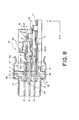
- Fig. 8 is a cross-sectional view of the connector taken along lines VIII-VIII of Fig. 2;
- Fig. 9 is a cross-sectional view of the connector taken along lines IX-IX of Fig. 6;
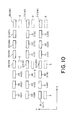
- Fig. 10 is a view schematically showing pin assignments in the connector of Fig. 1;
- Fig. 11 is a perspective view of an insulator housing as seen from the rear of the insulator, with a shell of the connector of Fig. 1 removed;
- Fig. 12 is a top plan view of the shell of the connector of Fig. 1, the shell being not fit with the insulator;
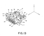
- Fig. 13 is a perspective view showing the connector of Fig. 1 with two coaxial cables being connected therewith;
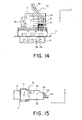
- Fig. 14 is a top plan view of the connector of Fig. 13, to which the coaxial cables are connected;
- Fig. 15 is a side view of the connector of Fig. 13, to which the coaxial cables are connected;
- Fig. 16 is a cross-sectional view of the connector taken along lines XVI-XVI of Fig. 2, to which the coaxial cables are connected;
- Fig. 17 is a view for use in describing the soldering process in the connector of Fig. 13;
- Fig. 18 is a cross-sectional view of the connector taken along lines XVIII-XVIII of Fig. 16;
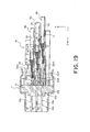
- Fig. 19 is a cross-sectional view of the connector taken along lines XIX-XIX of Fig. 16;
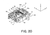
- Fig. 20 is a perspective view of the insulator housing as seen from the rear of the insulator housing, with the shell of the connector of Fig. 13 removed;
- Fig. 21 is a top plan view of a ground plate which is a modification of that of the connector of Fig. 1; and
- Fig. 22 is a cross-sectional view of the ground plate of the modification taken along lines XXII-XXII of Fig. 21.
-
- A connector according to an embodiment of the present invention is used in a system for transmitting high-frequency signals between a personal computer and its monitor.
- With reference to Figs. 1 to 9, the
connector 10 comprises a plurality ofcontacts insulator housing 30 supporting therein thecontacts shell 11 surrounding thecontacts insulator housing 30, and ground plates 1 (1a, 1b, 1c). The front end of theconnector 10 in a Z-direction is formed with a fitting portion for a mating connector, which is not shown. That is, the Z-direction is an insertion direction of the connector for the mating connector. On the other hand, cables carrying the high-speed signals are fixed on the rear side of theconnector 10 in the Z-direction. The installation of the cables is described later with reference to further drawings. In addition, akey 23 is provided, as a positioning means on the insertion for the mating connector, in the fitting portion of the front side in the Z-direction. Thekey 23 may be omitted, depending on the strength of theshell 11, thecontacts - In the present embodiment, the
connector 10 has twenty-fourcontacts reference numeral 21 are signal contacts for receiving or transmitting the differential pair of signals in the high-speed signal transmission system. That is, twoadjacent contacts 21 form a differential pair of contacts. The contacts depicted with thereference numeral 22 are ground contacts and are connected to corresponding ones of the ground plates 1, respectively. The contacts depicted with thereference numeral 24 are contacts which are used for a particular purpose other than high-speed signal transmission and a ground thereof. - The pin assignments of the
contacts connector 10, while an X-direction is from the left side to the right side of theconnector 10 as seen from the front side of theconnector 10. For the sake of clarity, a unique reference numeral is also assigned to every contact in Fig. 10, the unique reference numeral of each contact being shown in the parentheses corresponding to the contact. - With reference to Fig. 10, the
contacts contacts 101 to 108, 109 to 116, and 117 to 124. In other words, those contacts are arranged in eight columns each column including three contacts. In detail, the top row comprises three contacts 24 (101 to 103), four signal contacts 21 (104, 105, 107, 108) and one ground contact 22 (106). Among them, the two adjacent ones of signal contacts 21 (104, 105) are a differential pair of contacts, while the other two adjacent ones of the signal contacts 21 (107, 108) are another differential pair of contacts. These two differential pairs of contacts 21 (104, 105, 107, 108) share the ground contact 22 (106) disposed therebetween. The middle row comprises three contacts 24 (109 to 111), four signal contacts 21 (112, 113, 115, 116) and one ground contact 22 (114). Among them, two adjacent ones of the signal contacts 21 (112, 113) are a differential pair of contacts, while the other two adjacent signal contacts 21 (115, 116) are another differential pair of contacts. These two differential pairs of contacts 21 (112, 113, 115, 116) share the ground contact 22 (114) disposed therebetween. The bottom row comprises six signal contacts 21 (117, 118, 120, 121, 123, 124) and two ground contacts 22 (119, 122). Among them, two adjacent ones of the signal contacts 21 (117, 118) are a differential pair of contacts and one of the ground contacts 22 (119) corresponds to the differential pair of contacts. In addition, another two adjacent ones of the signal contacts 21 (120, 121) are another differential pair of contacts, while the other two adjacent ones of the signal contacts 21 (123, 124) are yet another pair of contacts. These two differential pairs of contacts 21 (120, 121, 123, 124) share the other one of ground contact 22 (122) disposed therebetween. - The
connector 10 further comprises seven conductive finger portions, conductive tab portion, or thin or narrowconductive members 3, which are shown by broken lines in Fig. 10. Everyconductive finger portion 3 is electrically connected through the ground plates 1 to the ground contacts 22 (106, 114, 118, 122). In addition, eachconductive finger portion 3 is arranged in the proximity of the signal contact 21 (104, 108, 112, 116, 117, 120, 124) which is positioned farther than the other signal contact 21 (105, 107, 113, 115, 118, 121, 123) from the ground contact 22 (106, 114, 119, 122) in each of the differential pairs of contacts. Specifically, each of the illustratedconductive finger portions 3 is located below the corresponding signal contact 21 (104, 108, 112, 116, 117, 120, 124), but may be located above thereof. Theconductive finger portions 3 compensate the impedance imbalance arising from the pin assignments of thesignal contacts 21 mentioned above, by adjusting the impedance of the signal contacts (104, 108, 112, 116, 117, 120, 124) to the substantially same level as that of the respective the other signal contacts (105, 107, 113, 115, 118, 121, 123). - Now, the structure of the connector is described in more detail with also reference to Figs. 11 and 12 in addition to Figs. 1-10.
- The
shell 11 comprises a fronttubular portion 13 for being fitted with the mating connector installed for example on a board of an electronic device not shown, a reartubular portion 14 having a shape of a rectangular tube, and twoflange portions 12 outwardly projecting opposite to each other in the X-direction from a joint portion between the fronttubular portion 13 and the reartubular portion 14. Theflange portions 12 havecircular holes 12a for screws used for fixing and ensuring the connection between theconnector 10 and the mating connector. The fronttubular portion 13 hasdimples 13a in its top and bottom outer surfaces, which serve to insure the electrical connection between theshell 11 of theconnector 10 and a shell of the mating connector. - The rear
tubular portion 14 is provided withedge portions tubular portion 14 is also provided with fiveopenings 14c in the top and the bottom walls thereof. Before theinsulator housing 30 is installed in the reartubular portion 14, the reartubular portion 14 is provided with hook portions 14c1 in the top and the bottom walls by making five U-shaped incisions or lance slits in the top and the bottom walls (e.g. see Fig. 12). When theinsulator housing 30 is installed in the reartubular portion 14, the hook portions 14c1 are bent toward the insulator housing installed in the reartubular portion 14, so that theopenings 14c are formed in the top and bottom walls of the reartubular portion 14 as mentioned above. Resultantly, the bent hook portions 14c1 are accommodated inrecess portions 30a (see Fig. 9 and 11) of theinsulator housing 30 thereby to fix theinsulator housing 30 to theshell 11. - The
insulator housing 30 comprises aguide housing 31 andground plate supporters guide housing 31 has a plate-like shape, in which thecontacts guide housing 31 has a plurality of through holes 35 (clearly shown in Fig. 7), a plurality of additional holes 34 (clearly shown in Figs. 5 and 8), and fiverecess portions 30a (clearly shown in Figs. 9 and 11). Therecess portions 30a are for accommodating therein the hook portions 14c1 of the reartubular portion 14, as mentioned above. In detail, theinsulator housing 30 with the ground plates 1 and thecontacts insulator housing 30 is fixed in theshell 11. - The through holes 35 are arranged in three rows each comprising eight holes. That is, the through
holes 35 have the same arrangement as thecontacts holes 35, thecontacts guide housing 31, so as to be suitably supported by theguide housing 31. - The
additional holes 34 are formed below the throughholes 35 corresponding to the signal contacts 21 (104, 108, 112, 116, 117, 120, 124) which are positioned away from the respective ground contacts 22 (106, 114, 119, 122), as clearly shown in Fig. 10. In theadditional holes 34, theconductive finger portions 3 are inserted from the rear side of theguide housing 31, so as to be suitably fitted in theguide housing 31. Specifically, theadditional holes 34 of the present embodiment are through holes. - The
ground plate supporters guide housing 31 and extend rearward (left-downward on the drawing sheet of Fig. 11) from theguide housing 31 in parallel to each other. The ground plates 1 (1a, 1b, 1c) bridge theground plate supporters ground plate supporters guide housing 31. Theguide housing 31 and theground plate supporters - The
contacts portions 21a (21a1, 21a2, 21a3) and 24a, respectively. Thetail portions 21a (21a1, 21a2, 21a3) and 24a are formed longer as being in the lower row of the three rows ofcontacts 21 and 24 (e.g. see Fig. 8). In the other words, thetail portions 21a (21 a1, 21a2, 21a3) and 24a are formed with increasing lengths in the order from the top to the bottom row of the three rows ofcontacts ground contacts 22 has first tothird portions first portion 22a extends straightly in the Z-direction and is supported by the throughholes 35 as described above. Thesecond portion 22b extends from thefirst portion 22a to make an obtuse angle with thefirst portion 22a as shown in Fig. 7. The third portion 22c1, 22c2, 22c3 extends from thesecond portion 22b to make an obtuse angle with thesecond portion 22b. As seen from Fig. 7, the first andthird portions 22a, 22c1, 22c2, 22c3 are substantially parallel to each other. The obtuse angle made by the first andsecond portions third portions 22b, 22c1, 22c2, 22c3. In addition, the third portions 22c1, 22c2, 22c3 of theground contacts 22 are formed longer as being in the lower row of the three contact rows (e.g. see Fig. 7). - In the embodiment described above, twenty-four (24)
contacts contacts contacts - As clearly shown in Figs. 7-9, the ground plates 1 (1a, 1b, 1c) comprise
cable holders 2,depressed portions 4, and bulges 5. On thedepressed portions 4, the third portions 22c1 to 22c3 of theground contacts 22 are disposed. Thedepressed portions 4 serve as banks to accommodate therein the solder material when the third portions 22c1 to 22c3 are connected to the ground plates 1a to 1c by soldering. Each of thebulges 5 is formed in the respective ground plate 1a to 1c so that a predetermined space becomes left between thebulge 5 and a corresponding one of thecontacts connector 10 is assembled. In order to adjust every signal path to have suitable impedance, the tail portion 21a1, 21a2, 21a3 straightly extends in parallel to the ground plate 1, and the predetermined space is set between tail portion 21a1, 21a2, 21a3 and the ground plate 1 for the same reason. Thebulge 5 serves to mount thereon at least one coaxial cable, especially, an inner insulator of the coaxial cable when the coaxial cable is connected to theconnector 10. Thebulge 5 has a predetermined height so as to adjust a center conductor of the coaxial connector to its position in which the center conductor can be connected to thecontact 21 suitably. Additionally referring to Fig. 11, each of thecable holders 2 has a cross-section of a half-loop, especially, a half of a substantial hexagon cylinder extending in the Z-direction. Each of thecable holders 2 is formed by making two slits in the ground plate 1 at positions spaced therebetween in the Z-direction and then pulling up the center of the portion sandwiched by the slits. Each of thecable holders 2 holds two coaxial cables and positions the heights of the coaxial cables in cooperation with a corresponding one of thebulges 5. - Next explanation is made of a connection of coaxial cables to the
connector 10, with reference also to Figs. 13 to 20. - A pair of
coaxial cables 50 are inserted into thecable holder 2 from the rear side of theconnector 10 withouter covers 53 of thecoaxial cables 50 being partially removed. Then, thecoaxial cables 50 are held at the outer covers 53 remained thereon by thecable holder 2, while theinner insulators 54 of thecoaxial cables 50 are mounted on thebulge 5 so that thecoaxial cables 50 are fixed in the Y-direction andcenter conductor 52 of thecoaxial cables 50 are adjusted to their positions in which thecenter conductors 52 can be suitably connected therespective contacts 21, as shown in Fig. 18. Twoouter conductors 51 of thecoaxial cables 50 are bundled and connected to a corresponding one of the third portions 22c1 to 22c3 of theground contacts 22 by soldering. At the time of soldering, thedepressed portion 4 receives thesolder material 7 so that thesolder material 7 does not have a bad influence on the impedance of thesignal contacts 21 positioned nearer to theground contact 22, as shown in Fig. 17. On the other hand, thecenter conductors 52 are soldered to twocorresponding signal contacts 21, respectively, withsoldering material 6, as shown in Fig. 17. - As seen from the figures, especially Figs. 18 and 19, the ground plate 1 is designed to substantially form a microstrip line together with the
contact 21, thecenter conductor 52 of thecoaxial cable 50, and the atmosphere (usually, the air) surrounding theconnector 10. The atmosphere serves as a dielectric portion of the microstrip line. Therefore, the impedance of the signal line is kept suitably. - Although a pair of coaxial cables are exampled as carriers of a pair of high-speed signals, a twin axial cable may be adopted as the carries of the pair of high-speed signals. In this case, it is preferable that a drain line of the twin axial cable is connected to the
ground contact 22. - In addition, a
single cable holder 2 has been explained to hold twocoaxial cables 50 but it may hold one coaxial cable. - Furthermore, the
ground contact 22 is formed integrally with the ground plate 1. By way of example, the ground plate 1 with theground contact 22 is shown in Figs. 21 and 22, which can be used in correspondence with theground contacts 22 of the top and the middle rows. As seen from the figures, each of the third portions of theground contacts 22 forms a part of the ground plate 1.
Claims (10)
- A connector for connecting at least first and second signal lines and a ground line with a mating connector fitable to said connector, said connector comprising a ground plate (1), an insulator (30), first and second contacts (21) being to be connected with said first and second signal lines, respectively, and a ground contact (22) being to be connected with said ground line, said ground plate (1) being electrically connected with said ground contact (22), said insulator (30) supporting therein said first and second contacts (21) and said ground contact (22) in accordance with predetermined pin assignments where said first and second contacts (21) and said ground contact (22) are arranged in the same row so that said first contact (21, 108) is positioned farther than said second contact (21, 108) from said ground contact (22, 106), said connector being characterized by further comprising a conductive finger portion (3) which is electrically connected with said ground plate (1) and which is arranged in the proximity of said first contact (21, 108).
- The connector according to claim 1, wherein said insulator (30) has first to third through holes (35) and an additional hole (34), said first to third through holes (35) being arranged in the same horizontal line so as to be inserted thereinto said first and second contacts (21), and said ground contact (22), respectively, in accordance with said predetermined pin assignments, said additional hole (34) accommodating therein said conductive finger portion (3) and being located above or below said first through (35) hole in the insulator (30), and/or wherein said first and second contacts (21) are a pair of positive and negative contacts or another pair of negative and positive contacts to form a differential pair of contacts, and/or wherein said conductive finger portion (3) is formed integrally with said ground plate (1).
- The connector according to claim 1 or 2, wherein said ground contact (22) comprises a first portion (22a) straightly extending in an insertion direction of the connector and supported by said insulator (30), a second portion (22b) extending from said first portion (22a) and making an obtuse angle with said first portion (22a), and a third portion (22c1, 22c2, 22c3) extending from said second portion (22b) and making an obtuse angle with said second portion (22b) so as to be parallel to said first portion (22a) and to be connected to said ground plate (1).
- The connector according to claim 3, wherein said ground contact (22) is formed integrally with said ground plate (1), or wherein said ground contact (22) is formed not integrally with said ground plate (1) but is electrically connected with said ground plate (1) for example by soldering, preferably said ground plate (1) comprising a depressed portion (4) for disposing thereon said third portion (22c1, 22c2, 22c3) of said ground contact (22).
- The connector according to claim 3 or 4, further comprising at least one column of ground contacts (22) each of which comprises said first to third portions (22a, 22b, 22c1, 22c2, 22c3), wherein said third portions (22c1, 22c2, 22c3) of said column of ground contacts (22) are preferably formed to be longer as being arranged lower in said column.
- The connector according to any one of claims 1 to 5, further comprising at least first and second columns of signal contacts, each of said signal contacts in said first column and each of said signal contacts in said second column serving as said first contacts and said second contacts (21) in each row of signals contacts, wherein said first signal contacts (21) of said first column preferably are provided with tail portions (21a1, 21a2, 21a3) formed to be longer as being arranged lower in said first column, while said second signal contacts (21) of said second column preferably are provided with tail portions (21a1, 21a2, 21a3) formed to be longer as being arranged lower in said second column.
- The connector according to any one of claims 1 to 6, for accommodating two center conductors (52) in first and second coaxial cables (50) as said first and second signal lines, respectively, said first and second coaxial cables (50) having outer conductors (51), and for accommodating said outer conductors (51) together as said ground line, said connector further comprising a cable holder (2) for holding at least one of said first and second coaxial cables (50), preferably, both coaxial cables (50).
- The connector according to claim 7, wherein said cable holder (2) is formed on said ground plate (1) and has a cross-section of a substantial half-loop.
- The connector according to any one of claims 1 to 6, a pair of said first and second signal lines and said ground line being provided as a twin axial cable, said connector further comprising a cable holder for holding said twin-axial cable, preferably, said cable holder being formed on said ground plate and having a cross-section of a substantial half-loop.
- The connector according to claims 7 to 9, said first and second coaxial cables (50) or said twin axial cable further comprising inner insulators (54) covering said first and second signal lines (52), wherein said ground plate (1) has a bulge (5) with a predetermined space left between said bulge (5) and tail portions (21a1, 21a2, 21a3) of a pair of said first and said second contacts (21), particularly, said bulge (5) being used to mount thereon said inner insulators (54) of said coaxial cables (50) or said twin axial cable and having a predetermined height so as to adjust said pair of first and second signal lines (52) to their positions in which said pair of first and second signal lines (52) can be connected to said pair of first and second signal contacts (21) suitably.
Applications Claiming Priority (2)
| Application Number | Priority Date | Filing Date | Title |
|---|---|---|---|
| JP2001306336A JP3564556B2 (en) | 2001-10-02 | 2001-10-02 | connector |
| JP2001306336 | 2001-10-02 |
Publications (2)
| Publication Number | Publication Date |
|---|---|
| EP1303011A1 true EP1303011A1 (en) | 2003-04-16 |
| EP1303011B1 EP1303011B1 (en) | 2005-04-13 |
Family
ID=19125989
Family Applications (1)
| Application Number | Title | Priority Date | Filing Date |
|---|---|---|---|
| EP02022112A Expired - Lifetime EP1303011B1 (en) | 2001-10-02 | 2002-10-02 | Electrical connector with reduced crosstalk |
Country Status (6)
| Country | Link |
|---|---|
| US (1) | US6817898B2 (en) |
| EP (1) | EP1303011B1 (en) |
| JP (1) | JP3564556B2 (en) |
| KR (1) | KR100532001B1 (en) |
| DE (1) | DE60203679T2 (en) |
| TW (1) | TW571465B (en) |
Cited By (3)
| Publication number | Priority date | Publication date | Assignee | Title |
|---|---|---|---|---|
| FR2914788A1 (en) * | 2007-04-05 | 2008-10-10 | Tyco Electronics France Sas So | ELECTRICAL CONTACTS ASSEMBLY |
| EP2360796A4 (en) * | 2008-12-17 | 2012-05-16 | Fujikura Ltd | Plug for universal serial bus connector, and connector assembly |
| EP3340395A1 (en) * | 2016-12-22 | 2018-06-27 | Dai-Ichi Seiko Co., Ltd. | Connector and production method thereof |
Families Citing this family (33)
| Publication number | Priority date | Publication date | Assignee | Title |
|---|---|---|---|---|
| TWM251379U (en) * | 2004-02-11 | 2004-11-21 | Comax Technology Inc | Grounding structure of electrical connector |
| US6964583B2 (en) * | 2004-02-13 | 2005-11-15 | Tyco Electronics Corporation | Connector having low frequency noise reducing ground |
| US7207807B2 (en) * | 2004-12-02 | 2007-04-24 | Tyco Electronics Corporation | Noise canceling differential connector and footprint |
| US20060121801A1 (en) * | 2004-12-02 | 2006-06-08 | Neven Pischl | High speed wired media connector with symmetric PCB interface |
| KR100651588B1 (en) | 2005-10-26 | 2006-11-29 | 주식회사 팬택앤큐리텔 | Connector for interface and electronics equipped with it |
| EP1961083B1 (en) * | 2005-11-23 | 2016-01-27 | Draeger Medical Systems, Inc. | A connector system |
| CN101038989A (en) * | 2006-03-14 | 2007-09-19 | 鸿富锦精密工业(深圳)有限公司 | Double difference pair cables |
| JP5001740B2 (en) * | 2007-07-20 | 2012-08-15 | ホシデン株式会社 | Electrical connector |
| US7744402B2 (en) * | 2007-08-13 | 2010-06-29 | Hon Hai Precision Ind. Co., Ltd. | Cable conductor assembly with protective stiffener |
| KR101578791B1 (en) * | 2008-06-04 | 2015-12-18 | 호시덴 가부시기가이샤 | Electric connector |
| JP4519182B2 (en) * | 2008-06-05 | 2010-08-04 | 日本航空電子工業株式会社 | connector |
| JP4567079B2 (en) | 2008-08-22 | 2010-10-20 | 日本航空電子工業株式会社 | connector |
| US7736183B2 (en) * | 2008-10-13 | 2010-06-15 | Tyco Electronics Corporation | Connector assembly with variable stack heights having power and signal contacts |
| US7896698B2 (en) * | 2008-10-13 | 2011-03-01 | Tyco Electronics Corporation | Connector assembly having multiple contact arrangements |
| US7740489B2 (en) * | 2008-10-13 | 2010-06-22 | Tyco Electronics Corporation | Connector assembly having a compressive coupling member |
| US7637777B1 (en) | 2008-10-13 | 2009-12-29 | Tyco Electronics Corporation | Connector assembly having a noise-reducing contact pattern |
| US7867032B2 (en) * | 2008-10-13 | 2011-01-11 | Tyco Electronics Corporation | Connector assembly having signal and coaxial contacts |
| US7972151B2 (en) * | 2009-01-05 | 2011-07-05 | Hon Hai Precision Ind. Co., Ltd. | Electrical connector with improved arrangement of ground and signal contacts |
| US8113851B2 (en) * | 2009-04-23 | 2012-02-14 | Tyco Electronics Corporation | Connector assemblies and systems including flexible circuits |
| US7918683B1 (en) | 2010-03-24 | 2011-04-05 | Tyco Electronics Corporation | Connector assemblies and daughter card assemblies configured to engage each other along a side interface |
| US8947638B2 (en) * | 2010-12-03 | 2015-02-03 | Asml Netherlands B.V. | Actuation system and lithographic apparatus |
| US9203176B2 (en) * | 2012-07-20 | 2015-12-01 | Advanced-Connetek Inc. | Plug connector |
| CN202737250U (en) * | 2012-07-20 | 2013-02-13 | 连展科技电子(昆山)有限公司 | Connector plug structure |
| CN103346436B (en) * | 2013-06-25 | 2018-04-10 | 连展科技电子(昆山)有限公司 | Plug connector |
| US9124008B2 (en) * | 2013-08-29 | 2015-09-01 | Tyco Electronics Corporation | Electrical connector |
| TW201517418A (en) * | 2013-10-18 | 2015-05-01 | Kuang Ying Comp Equipment Co | Electric coupler |
| JP6330587B2 (en) * | 2014-09-04 | 2018-05-30 | 株式会社オートネットワーク技術研究所 | Communication connector |
| EP3285338A4 (en) * | 2015-04-14 | 2018-11-14 | Mitsubishi Electric Corporation | Multi-pole connector, connector device, case, and method of connecting cable to multi-pole connector |
| KR101616351B1 (en) * | 2015-10-29 | 2016-04-28 | 현대산업 주식회사 | Connecting terminal for connector |
| US10673182B2 (en) | 2015-12-07 | 2020-06-02 | Fci Usa Llc | Electrical connector having electrically commoned grounds |
| TWI738618B (en) | 2015-12-07 | 2021-09-01 | 新加坡商安姆芬諾爾富加宜(亞洲)私人有限公司 | Electrical connector having electrically commoned grounds |
| JP7404142B2 (en) * | 2020-04-17 | 2023-12-25 | 日本航空電子工業株式会社 | Connectors, harnesses and connector assemblies |
| US12198174B2 (en) * | 2021-02-22 | 2025-01-14 | Te Connectivity Germany Gmbh | Connector configurator |
Citations (2)
| Publication number | Priority date | Publication date | Assignee | Title |
|---|---|---|---|---|
| EP1052739A2 (en) * | 1999-05-13 | 2000-11-15 | Berg Electronics Manufacturing B.V. | Shielded header |
| US6280209B1 (en) * | 1999-07-16 | 2001-08-28 | Molex Incorporated | Connector with improved performance characteristics |
Family Cites Families (10)
| Publication number | Priority date | Publication date | Assignee | Title |
|---|---|---|---|---|
| US5380216A (en) * | 1992-05-11 | 1995-01-10 | The Whitaker Corporation | Cable backpanel interconnection |
| JPH07135049A (en) * | 1993-11-10 | 1995-05-23 | Kel Corp | Shielded connector |
| US5509827A (en) * | 1994-11-21 | 1996-04-23 | Cray Computer Corporation | High density, high bandwidth, coaxial cable, flexible circuit and circuit board connection assembly |
| US5718607A (en) | 1996-03-01 | 1998-02-17 | Molex Incorporated | System for terminating the shield of a high speed cable |
| JP3363804B2 (en) * | 1998-10-06 | 2003-01-08 | ケル株式会社 | Male and female mating connectors |
| EP1196967B1 (en) * | 1999-07-16 | 2004-09-29 | Molex Incorporated | Impedance-tuned connector |
| US6524135B1 (en) * | 1999-09-20 | 2003-02-25 | 3M Innovative Properties Company | Controlled impedance cable connector |
| US6350134B1 (en) * | 2000-07-25 | 2002-02-26 | Tyco Electronics Corporation | Electrical connector having triad contact groups arranged in an alternating inverted sequence |
| JP3495007B2 (en) * | 2001-03-14 | 2004-02-09 | 日本航空電子工業株式会社 | High-speed transmission connector |
| US6540559B1 (en) * | 2001-09-28 | 2003-04-01 | Tyco Electronics Corporation | Connector with staggered contact pattern |
-
2001
- 2001-10-02 JP JP2001306336A patent/JP3564556B2/en not_active Expired - Fee Related
-
2002
- 2002-09-30 US US10/260,889 patent/US6817898B2/en not_active Expired - Lifetime
- 2002-10-01 TW TW091122639A patent/TW571465B/en not_active IP Right Cessation
- 2002-10-01 KR KR10-2002-0059721A patent/KR100532001B1/en not_active Expired - Fee Related
- 2002-10-02 DE DE60203679T patent/DE60203679T2/en not_active Expired - Lifetime
- 2002-10-02 EP EP02022112A patent/EP1303011B1/en not_active Expired - Lifetime
Patent Citations (2)
| Publication number | Priority date | Publication date | Assignee | Title |
|---|---|---|---|---|
| EP1052739A2 (en) * | 1999-05-13 | 2000-11-15 | Berg Electronics Manufacturing B.V. | Shielded header |
| US6280209B1 (en) * | 1999-07-16 | 2001-08-28 | Molex Incorporated | Connector with improved performance characteristics |
Cited By (6)
| Publication number | Priority date | Publication date | Assignee | Title |
|---|---|---|---|---|
| FR2914788A1 (en) * | 2007-04-05 | 2008-10-10 | Tyco Electronics France Sas So | ELECTRICAL CONTACTS ASSEMBLY |
| US7753730B2 (en) | 2007-04-05 | 2010-07-13 | Tyco Electronics France Sas | Electrical contact holder assembly |
| EP2360796A4 (en) * | 2008-12-17 | 2012-05-16 | Fujikura Ltd | Plug for universal serial bus connector, and connector assembly |
| US8460035B2 (en) | 2008-12-17 | 2013-06-11 | Fujikura Ltd. | Connector assembly including a cable with a USB 3.0 signal line, a USB 2.0 signal line, a power line and a ground line |
| EP3340395A1 (en) * | 2016-12-22 | 2018-06-27 | Dai-Ichi Seiko Co., Ltd. | Connector and production method thereof |
| US10181683B2 (en) | 2016-12-22 | 2019-01-15 | Dai-Ichi Seiko Co., Ltd. | Connector and production method thereof |
Also Published As
| Publication number | Publication date |
|---|---|
| US20030064614A1 (en) | 2003-04-03 |
| KR100532001B1 (en) | 2005-12-02 |
| EP1303011B1 (en) | 2005-04-13 |
| JP2003115358A (en) | 2003-04-18 |
| DE60203679D1 (en) | 2005-05-19 |
| JP3564556B2 (en) | 2004-09-15 |
| US6817898B2 (en) | 2004-11-16 |
| DE60203679T2 (en) | 2006-01-19 |
| TW571465B (en) | 2004-01-11 |
| KR20030028713A (en) | 2003-04-10 |
Similar Documents
| Publication | Publication Date | Title |
|---|---|---|
| EP1303011B1 (en) | Electrical connector with reduced crosstalk | |
| US7651379B1 (en) | Cable assembly with improved termination disposition | |
| US11652325B2 (en) | Cable connector system | |
| US6764342B2 (en) | Electrical connector for balanced transmission cables with module for positioning cables | |
| US10923843B1 (en) | Receptacle assembly having cabled receptacle connector | |
| JP2538137B2 (en) | Connector assembly | |
| CN101828308B (en) | Electrical Connector Assembly | |
| CN102138256B (en) | Carrier assembly and system configured to commonly ground a header | |
| US20040014360A1 (en) | Modular coaxial electrical interconnect system and method of making the same | |
| EP2487761B1 (en) | Telecommunications connector | |
| US20040043661A1 (en) | Connector apparatus | |
| JPH06103635B2 (en) | Connector with ground structure | |
| US12327948B2 (en) | High density coupling panel | |
| US10868392B2 (en) | Ground commoning conductors for electrical connector assemblies | |
| US11303053B2 (en) | Connector assembly | |
| CN115410768A (en) | Cable shield construction for electrical installations | |
| US12334659B2 (en) | Connection body and harness | |
| JP2019133809A (en) | Electric connector | |
| US20070015414A1 (en) | Enhanced jack with plug engaging printed circuit board | |
| CN112448195A (en) | Cable assembly with improved cable retention | |
| CN111755861A (en) | Connector with a locking member | |
| CN120834472A (en) | Ground bus for a cable card assembly of an electrical connector | |
| CN107732578A (en) | cable connector | |
| CN121642603A (en) | Electrical connectors | |
| CN122073352A (en) | Electrical shielding arrangement for high-speed electrical connectors |
Legal Events
| Date | Code | Title | Description |
|---|---|---|---|
| PUAI | Public reference made under article 153(3) epc to a published international application that has entered the european phase |
Free format text: ORIGINAL CODE: 0009012 |
|
| AK | Designated contracting states |
Designated state(s): AT BE BG CH CY CZ DE DK EE ES FI FR GB GR IE IT LI LU MC NL PT SE SK TR |
|
| AX | Request for extension of the european patent |
Extension state: AL LT LV MK RO SI |
|
| 17P | Request for examination filed |
Effective date: 20031014 |
|
| AKX | Designation fees paid |
Designated state(s): DE FI FR GB |
|
| 17Q | First examination report despatched |
Effective date: 20040127 |
|
| GRAP | Despatch of communication of intention to grant a patent |
Free format text: ORIGINAL CODE: EPIDOSNIGR1 |
|
| GRAS | Grant fee paid |
Free format text: ORIGINAL CODE: EPIDOSNIGR3 |
|
| GRAA | (expected) grant |
Free format text: ORIGINAL CODE: 0009210 |
|
| AK | Designated contracting states |
Kind code of ref document: B1 Designated state(s): DE FI FR GB |
|
| REG | Reference to a national code |
Ref country code: GB Ref legal event code: FG4D |
|
| REG | Reference to a national code |
Ref country code: IE Ref legal event code: FG4D |
|
| REF | Corresponds to: |
Ref document number: 60203679 Country of ref document: DE Date of ref document: 20050519 Kind code of ref document: P |
|
| ET | Fr: translation filed | ||
| PLBE | No opposition filed within time limit |
Free format text: ORIGINAL CODE: 0009261 |
|
| STAA | Information on the status of an ep patent application or granted ep patent |
Free format text: STATUS: NO OPPOSITION FILED WITHIN TIME LIMIT |
|
| 26N | No opposition filed |
Effective date: 20060116 |
|
| PGFP | Annual fee paid to national office [announced via postgrant information from national office to epo] |
Ref country code: GB Payment date: 20131002 Year of fee payment: 12 Ref country code: DE Payment date: 20130925 Year of fee payment: 12 Ref country code: FR Payment date: 20131009 Year of fee payment: 12 |
|
| PGFP | Annual fee paid to national office [announced via postgrant information from national office to epo] |
Ref country code: FI Payment date: 20131010 Year of fee payment: 12 |
|
| REG | Reference to a national code |
Ref country code: DE Ref legal event code: R119 Ref document number: 60203679 Country of ref document: DE |
|
| GBPC | Gb: european patent ceased through non-payment of renewal fee |
Effective date: 20141002 |
|
| PG25 | Lapsed in a contracting state [announced via postgrant information from national office to epo] |
Ref country code: GB Free format text: LAPSE BECAUSE OF NON-PAYMENT OF DUE FEES Effective date: 20141002 Ref country code: DE Free format text: LAPSE BECAUSE OF NON-PAYMENT OF DUE FEES Effective date: 20150501 Ref country code: FI Free format text: LAPSE BECAUSE OF NON-PAYMENT OF DUE FEES Effective date: 20141002 |
|
| REG | Reference to a national code |
Ref country code: FR Ref legal event code: ST Effective date: 20150630 |
|
| PG25 | Lapsed in a contracting state [announced via postgrant information from national office to epo] |
Ref country code: FR Free format text: LAPSE BECAUSE OF NON-PAYMENT OF DUE FEES Effective date: 20141031 |