EP1301001A2 - Transmission with constellations of a size other than a power of two - Google Patents
Transmission with constellations of a size other than a power of two Download PDFInfo
- Publication number
- EP1301001A2 EP1301001A2 EP02021895A EP02021895A EP1301001A2 EP 1301001 A2 EP1301001 A2 EP 1301001A2 EP 02021895 A EP02021895 A EP 02021895A EP 02021895 A EP02021895 A EP 02021895A EP 1301001 A2 EP1301001 A2 EP 1301001A2
- Authority
- EP
- European Patent Office
- Prior art keywords
- signals
- digits
- modulator
- communication data
- ary
- Prior art date
- Legal status (The legal status is an assumption and is not a legal conclusion. Google has not performed a legal analysis and makes no representation as to the accuracy of the status listed.)
- Withdrawn
Links
Images




Classifications
-
- H—ELECTRICITY
- H04—ELECTRIC COMMUNICATION TECHNIQUE
- H04L—TRANSMISSION OF DIGITAL INFORMATION, e.g. TELEGRAPHIC COMMUNICATION
- H04L27/00—Modulated-carrier systems
- H04L27/32—Carrier systems characterised by combinations of two or more of the types covered by groups H04L27/02, H04L27/10, H04L27/18 or H04L27/26
- H04L27/34—Amplitude- and phase-modulated carrier systems, e.g. quadrature-amplitude modulated carrier systems
-
- H—ELECTRICITY
- H04—ELECTRIC COMMUNICATION TECHNIQUE
- H04L—TRANSMISSION OF DIGITAL INFORMATION, e.g. TELEGRAPHIC COMMUNICATION
- H04L25/00—Baseband systems
- H04L25/38—Synchronous or start-stop systems, e.g. for Baudot code
- H04L25/40—Transmitting circuits; Receiving circuits
- H04L25/49—Transmitting circuits; Receiving circuits using code conversion at the transmitter; using predistortion; using insertion of idle bits for obtaining a desired frequency spectrum; using three or more amplitude levels ; Baseband coding techniques specific to data transmission systems
- H04L25/4917—Transmitting circuits; Receiving circuits using code conversion at the transmitter; using predistortion; using insertion of idle bits for obtaining a desired frequency spectrum; using three or more amplitude levels ; Baseband coding techniques specific to data transmission systems using multilevel codes
-
- H—ELECTRICITY
- H04—ELECTRIC COMMUNICATION TECHNIQUE
- H04L—TRANSMISSION OF DIGITAL INFORMATION, e.g. TELEGRAPHIC COMMUNICATION
- H04L27/00—Modulated-carrier systems
- H04L27/18—Phase-modulated carrier systems, i.e. using phase-shift keying
Definitions
- the present invention relates to a modulator, a communication system, and a modulation program, in which communication is executed by a multilevel modulation in digital microwave communication.
- a multilevel modulation is a modulation system using especially for such as a digital microwave communication, and conventionally, there are a quadrature amplitude modulation (QAM) system and a phase shift keying (PSK) system.
- QAM quadrature amplitude modulation
- PSK phase shift keying
- systems based on such as 4QAM, 16QAM, 32QAM, 64QAM, 128QAM, and 256QAM, ... and BPSK (2PSK), QPSK (4PSK), and 8PSK ... are used.
- the number of multilevel of the multilevel signal is made to be a value of the n th power of 2, such as 2, 4, 8, 16, ....
- the difficulty to realize the complex circuit structure at a modulation system in which the number of multilevel is made to be a value except the values of the n th power of 2, has been lessened by the recent progress in the IC technology.
- Japanese Patent Application Laid-Open No. HEI 4-196945 discloses a multilevel modulation and demodulation communication method and a system thereof.
- a system in which an input data string is allocated to a modulation symbol being general 2 or more value, is proposed.
- a general structure of a multilevel modulation using the number of multilevel except the values of the n th power of 2 is only shown.
- a technical report shows an apparatus, a communication system, a program, and a method for a multilevel modulation and demodulation.
- the numbers of multilevel are about 2 ⁇ (p + 0.5), and a technology, in which multilevel modulations such as 3PSK, 6PSK, 12PSK, ... are realized, is proposed.
- a technical report shows an apparatus, a communication system, a program, and a method for a multilevel modulation and demodulation.
- the numbers of multilevel are about 2 ⁇ (p + 0.25), and a technology, in which multilevel modulations such as 10QAM, 20QAM, 40QAM, ... are realized, is proposed.
- a modulator, a communication system, and a modulation program, in which communication by 5PSK is realized are provided, by solving the problems at the conventional technologies mentioned above.
- a modulator which applies a phase modulation to communication data.
- inputted communication data are converted into plural multilevel signals of predetermined amount of data, and modulation signals based on the converted plural multilevel signals of the predetermined amount of data are outputted sequentially as modulated waves.
- the modulator provides a storing circuit that stores the inputted communication data, a converting circuit that converts the communication data storing in the storing circuit into the plural multilevel signals of the predetermined amount of data, and a multilevel modulator that generates the modulation signals based on the plural multilevel signals of the predetermined amount of data converted at the converting circuit, and outputs the modulated waves.
- each of b, C, m, and N is defined as one of integers, and the inputted communication data of C-ary signals are extracted b digits each sequentially from the storing circuit, and extracted C-ary signals of b digits are converted into N-ary signals of m digits sequentially at the converting circuit.
- the integer C being the number of multilevel of inputting communication data is 2.
- the value of the m th power of N is larger than the value of the b th power of C, and also the value of the m th power of N is close enough to the value of the b th power of C.
- each value of the integers b, m, and N is decided, based on a currently usable transmission band and a transmission rate to be required for communication data to be transmitted, and the inputted communication data are converted into N-ary signals of m digits, based on the decision.
- the communication data of C-ary signals are inputted to the modulator in series.
- the communication data of C-ary signals are inputted to the modulator in parallel b digits each.
- a communication system which executes communication by using multilevel signals.
- the communication system provides a modulator, which applies a phase modulation to communication data, and a demodulator.
- the modulator converts inputted communication data into plural multilevel signals of predetermined amount of data sequentially, and transmits modulation signals based on the converted plural multilevel signals of the predetermined amount of data as modulated waves to the demodulator sequentially.
- each of b, C, m, and N is defined as one of integers, and the inputted communication data of C-ary signals are extracted b digits each sequentially, and extracted C-ary signals of b digits are converted into N-ary signals of m digits sequentially at the modulator.
- the integer C being the number of multilevel of inputting communication data is 2.
- the value of the m th power of N is larger than the value of the b th power of C, and also the value of the m th power of N is close enough to the value of the b th power of C.
- each value of the integers b, m, and N is decided, based on a currently usable transmission band and a transmission rate to be required for communication data to be transmitted, and the inputted communication data are converted into N-ary signals of m digits, based on the decision.
- the communication data of C-ary signals are inputted to the modulator in series.
- the communication data of C-ary signals are inputted to the modulator in parallel b digits each.
- a modulation program which applies a phase modulation to communication data by controlling a computer.
- inputted communication data are converted into plural multilevel signals of predetermined amount of data, and modulation signals based on the converted plural multilevel signals of the predetermined amount of data are outputted sequentially as modulated waves.
- each of b, C, m, and N is defined as one of integers, and the inputted communication data of C-ary signals are extracted b digits each sequentially, and extracted C-ary signals of b digits are converted into N-ary signals of m digits sequentially.
- the integer C being the number of multilevel of inputting communication data is 2.
- the value of the m th power of N is larger than the value of the b th power of C, and also the value of the m th power of N is close enough to the value of the b th power of C.
- each value of the integers b, m, and N is decided, based on a currently usable transmission band and a transmission rate to be required for communication data to be transmitted, and the inputted communication data are converted into N-ary signals of m digits, based on the decision.
- the communication data of C-ary signals are inputted in series.
- the communication data of C-ary signals are inputted in parallel b digits each.
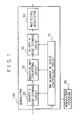
- Fig. 1 is a block diagram showing a structure of a modulator 100 at a first embodiment of the present invention.
- the modulator 100 at the first embodiment of the present invention receives binary signals being general communication signals and converts the binary signals into N-ary signals, and generates modulation signals based on the converted N-ary signals and outputs modulated waves.
- the modulator 100 provides the number of digits controlling circuit 10, a binary b digit storing circuit 20, a binary/N-ary converting circuit 30, an N-ary m digit storing circuit 40, and a multilevel modulator 50.
- each of the values of b, N, and m shows one of integers.
- N being the number of multilevel of the output signal
- 3 or more integer is used, and each value of the b and m ( ⁇ 1) is decided in the conditions that 2 ⁇ b ⁇ N ⁇ m, and the value of N ⁇ m becomes a close value to the value of 2 ⁇ b.
- the binary b digit storing circuit 20 stores inputted communication data (binary signals), and stores the binary signals b digits each.
- the binary/N-ary converting circuit 30 extracts the communication data of the binary signals storing in the binary b digit storing circuit 20 b digits each, and converts the extracted binary signals into N-ary signals of m digits.
- the N-ary m digit storing circuit 40 (transmitting data storing circuit) stores the N-ary signals of m digits converted at the binary/N-ary converting circuit 30.
- the multilevel modulator 50 generates modulation signals based on the converted N-ary signals storing in the N-ary m digit storing circuit 40, and outputs modulated waves.
- the multilevel modulator 50 outputs multilevel signals by such as the PSK and the QAM.
- the number of digits controlling circuit 10 controls each of the circuits in the modulator 100.
- a modulation program 90 shown in Fig. 1 is explained later.
- Fig. 2 is a flowchart showing the operation of the modulator 100 at the first embodiment of the present invention.
- communication data of binary signals are inputted to the input terminal of the modulator 100, and the binary b digit storing circuit 20 stores the inputted communication data b digits each sequentially.
- the binary b digit storing circuit 20 stores the inputted communication data as the binary signals of b digits (step 301).
- the binary/N-ary converting circuit 30 converts the binary signals of b digits storing in the binary b digit storing circuit 20 into N-ary signals of m digits sequentially (step 302).
- the N-ary m digit storing circuit 40 stores these converted N-ary signals of m digits sequentially, and the multilevel modulator 50 generates modulation signals based on the stored N-ary signals, and outputs modulated waves (step 303).
- the number of digits controlling circuit 10 adjusts the clock rates of the inputted binary signals and the outputting N-ary signals. For example, the number of digits controlling circuit 10 controls so that the N-ary signals are outputted at the clock rate of (m/b) times of the clock rate of the inputted binary signals.
- each integer of the b, N, and m must satisfy the condition of 2 ⁇ b ⁇ N ⁇ m.
- the 2 ⁇ b is smaller than the N ⁇ m largely, the amount of information per symbol of the converted N-ary signals becomes small, and the efficiency at communication becomes low. Therefore, it is desirable that the value of 2 ⁇ b is close enough to the value of N ⁇ m.
- the conversion operation can be executed uniquely by adopting the operation converting the number expression from the binary numbers to the N-ary numbers.
- the general communication data of the inputted binary signals are converted into the N-ary signals of m digits from the binary signals of b digits, and the modulation signals are generated based on the N-ary signals, and the modulated waves are outputted.
- the binary b digit storing circuit 20 sequentially stores the inputted binary signals by gathering them b digits each, and the binary signals of b digits are converted into the N-ary signals of m digits at the binary/N-ary converting circuit 30.
- the inputted communication data are binary signals inputting in parallel b digits each
- the inputted binary signals of b digits are converted into the N-ary signals of m digits sequentially every each clock, this method can be adopted.
- the converted N-ary signals of m digits can be outputted as the N-ary signals of m digits in parallel.
- Fig. 3 is a block diagram showing a structure of a communication system 300 using the modulator 100 at the first embodiment of the present invention.
- the N-ary signals applied the phase modulation at the modulator 100 in a transmitter 110 are received at a demodulator 200 in a receiver 210, and the received N-ary signals are converted into the binary signals at the demodulator 200 by applied the phase modulation.
- the conversion operation from the N-ary signals to the binary signals at the demodulator 200 can be executed by applying the reverse operation at the modulator 100.
- the transmitted N-ary signals are stored, and the N-ary signals of m digits are sequentially converted into the binary signals of b digits.
- the conversion operation at the demodulator 200 As mentioned above, the amount of information, which can be shown by the N-ary signals of m digits before converted, is larger than the amount of information, which can be shown by the binary signals of b digits after converted.
- the N-ary signals before converted are signals generated by that the binary signals of b digits were converted into the N-ary signals of m digits, the binary signals after converted can be obtained uniquely without the shortage of information.
- the conversion operation at the demodulator 200 as the same as the conversion operation at the modulator 100, the conversion operation can be executed by adopting the operation converting the number expression from the N-ary numbers to the binary numbers.
- Fig. 4 is a block diagram showing a structure of a modulator 100a at a first example of the first embodiment of the present invention.
- the modulator 100a provides a binary 11 digit storing circuit 20a that stores inputted binary signals 11 digits each, a binary/ternary converting circuit 30a that converts the binary signals of 11 digits into ternary signals of 7 digits, a ternary 7 digit storing circuit 40a that stores the converted ternary signals of 7 digits sequentially, a multilevel modulator 50a that generates modulation signals based on the ternary signals of 7 digits and outputs modulated waves, and the number of digits controlling circuit 10a that controls these three circuits.
- a modulation program 90a shown in Fig. 4 is explained later.
- the binary 11 digit storing circuit 20a receives communication data of binary signals inputted at the input terminal of the modulator 100a, and stores the binary signals 11 digits each.
- the binary/ternary converting circuit 30a converts the binary signals of 11 digits storing in the binary 11 digit storing circuit 20a into the ternary signals of 7 digits. This conversion operation can be executed uniquely, for example, by using a method converting the binary signals of 11 digits into the ternary signals of 7 digits.
- the ternary 7 digit storing circuit 40a stores the converted ternary signals of 7 digits, and the multilevel modulator 50a generates modulation signals based on the ternary signals of 7 digits and outputs modulated waves.
- the number of digits controlling circuit 10a controls so that the ternary signals are outputted at a clock rate of (7/11) times of the clock rate of the inputted binary signals, and also controls so that the number of digits of the binary signals is made to be 11 digits and the number of digits of the ternary signals is made to be 7 digits.
- the modulator 100a receives binary signals that are inputted in parallel 11 digits each, and converts the binary signals of 11 digits inputted at each clock into the ternary signals of 7 digits sequentially, and outputs the ternary signals in parallel 7 digits each.
- Fig. 5 is a timing chart showing the operation of the modulator 100a at the first example of the first embodiment of the present invention.
- the inputted binary signals are stored in the binary 11 digit storing circuit 20a as the binary signals of 11 digits.
- the binary/ternary converting circuit 30a converts the binary signals of 11 digits storing in the binary 11 digit storing circuit 20a into the ternary signals of 7 digits.
- the ternary 7 digit storing circuit 40a stores these converted ternary signals of 7 digits.
- the multilevel modulator 50a applies time multiplexing to these parallel signals of 7 digits and generates modulation signals being ternary signals in one string in its time and outputs these modulation signals as modulated waves.
- FIG. 6 is a block diagram showing a structure of a modulator 100b at the second example of the first embodiment of the present invention.
- the modulator 100b provides a binary 9 digit storing circuit 20b that stores inputted binary signals 9 digits each, a binary/5-ary converting circuit 30b that converts the binary signals of 9 digits into 5-ary signals of 4 digits, a 5-ary 4 digit storing circuit 40b that stores the converted 5-ary signals of 4 digits sequentially, a multilevel modulator 50b that generates modulation signals based on the 5-ary signals of 4 digits and outputs modulated waves, and the number of digits controlling circuit 10b that controls these three circuits.
- a modulation program 90b shown in Fig. 6 is explained later.
- the binary 9 digit storing circuit 20b receives communication data of binary signals inputted at the input terminal of the modulator 100b, and stores the binary signals 9 digits each.
- the binary/5-ary converting circuit 30b converts the binary signals of 9 digits storing in the binary 9 digit storing circuit 20b into the 5-ary signals of 4 digits. This conversion operation can be executed uniquely, for example, by using a method converting the binary signals of 9 digits into the 5-ary signals of 4 digits.
- the 5-ary 4 digit storing circuit 40b stores the converted 5-ary signals of 4 digits, and the multilevel modulator 50b generates modulation signals based on the 5-ary signals of 4 digits and outputs modulated waves.
- the number of digits controlling circuit 10b controls so that the 5-ary signals are outputted at a clock rate of (4/9) times of the clock rate of the inputted binary signals, and also controls so that the number of digits of the binary signals is made to be 9 digits and the number of digits of the 5-ary signals is made to be 4 digits.
- 5PSK is realized.
- the transmission band of the BPSK is shown as " 1 "
- the transmission band of QPSK is shown as " 1/2 "
- the transmission band of the 5PSK at this example of the present invention can be made to be " 1/2.25 ".
- the communication can be executed effectively by utilizing the transmission band more effectively than at the conventional technology.
- a case is studied, in this case, it is desired that communication data are transmitted at the transmission rate of 100 Mbps, and only the frequency band which can transmits at the modulation rate of 45M (symbol/sec.) exists.
- the number of multilevel for the multilevel modulation is selected from many values such as 4, 8, 16, ...that are separated largely among them.
- the modulation rate becomes 33.3 M (symbol/sec.), and the frequency band has too many margins, and at the QPSK (4PSK), the modulation rate becomes 50M (symbol/sec.), and the frequency band cannot be used because of its shortage.
- a signal to noise ratio (S/N ratio) for realizing a required error rate can be improved by using the transmission band widely without a surplus. Therefore, it is important to match the number of bits per symbol with the allowable transmission band.
- S/N ratio signal to noise ratio
- the S/N ratio is required to be 18.91 dB for achieving the error rate of the minus sixth power of 10.
- the same error rate can be achieved by the S/N ratio of 15.1 dB.
- the transmission band can be utilized effectively, and further, the efficiency utilizing the electric power can be improved.
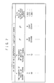
- Fig. 7 is a table showing various parameters at the modulator 100a in the first example of the first embodiment of present invention.
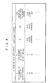
- Fig. 8 is a table showing various parameters at the modulator 100b in the second example of the first embodiment of present invention.
- Fig. 9 is a diagram showing the number of transmission bits per symbol in the comparison between the conventional technology and the first and second examples of the first embodiment of the present invention.
- Fig. 10 is a block diagram showing a structure of a modulator 100c at the second embodiment of the present invention.
- the inputted communication data are binary signals being the general communication signals.
- the inputted communication data are C-ary signals instead of the binary signals, and the inputted C-ary signals are converted into N-ary signals and modulation signals based on the converted N-ary signals are outputted as modulated waves.
- the modulator 100c receives multilevel signals and converts the received multilevel signals into multilevel signal being different from the received multilevel signals and generates modulation signals based on the converted multilevel signals and outputs the modulation signals as modulated waves. This operation can be executed at the second embodiment of the present invention.
- the modulator 100c outputs modulation signals by converting C-ary signals into N-ary signals by applying a phase modulation.
- the number of multilevel C is an integer such as 2, 3, 4, 5, ....
- the modulator 100c provides a C-ary b digit storing circuit 20c, a C-ary/N-ary converting circuit 30c, a N-ary m digit storing circuit 40c, a multilevel modulator 50c, and the number of digits controlling circuit 10c.
- a modulation program 90c shown in Fig. 10 is explained later.
- the C-ary b digit storing circuit 20c stores C-ary signals of b digits by extracting b digits each from the received communication data of the C-ary signals inputted at the input terminal of the modulator 100c.
- the C-ary/N-ary converting circuit 30c converts the C-ary signals of b digits storing in the C-ary b digit storing circuit 20c into the N-ary signals of m digits. This conversion operation can be executed uniquely, for example, by using a method converting the C-ary signals of b digits into the N-ary signals of m digits.
- the N-ary m digit storing circuit 40c stores the converted N-ary signals of m digits, and the multilevel modulator 50c generates modulation signals based on the N-ary signals of m digits and outputs the modulation signals as modulated waves.
- the number of digits controlling circuit 10c controls so that the N-ary signals are outputted at a clock rate of (m/b) times of the clock rate of the inputted C-ary signals, and also controls so that the number of digits of the C-ary signals is made to be b digits and the number of digits of the N-ary signals is made to be m digits.
- the modulator 100c receives multilevel signals and converts the received multilevel signals into multilevel signals being different from the received multilevel signals and outputs the modulation signals based on the converted multilevel signals as the modulated waves.
- the modulator itself decides the value of each integer of b, m, and N, based on the transmission band, which can be used currently, and the transmission rate to be required for transmitting communication data. And the modulator outputs modulation signals based on N-ary signals of m digits by converting the communication data into the N-ary of m digits based on the decided values of the b, m, and N.
- the operation deciding the value of each integer of the b, m, and N is executed by the number of digits controlling circuit.
- the inputting communication data are binary signals.
- the modulator receives binary signals.
- the modulator at the third embodiment of the present invention has a function, which the number of multilevel N of the N-ary signals for the phase modulation can be set freely. And at the changing operation of the number of multilevel N, the value of each integer of the b, m, and N are decided, by obtaining the transmission rate (for example, 100M bps) to be required for transmitting communication data, and by detecting the modulation rate of the transmission band (for example, 45M symbol/sec.).
- the transmission rate for example, 100M bps
- the modulation rate of the transmission band for example, 45M symbol/sec.
- a method in which the values of b and m are selected automatically based on the predetermined selecting method.
- the values of b and m are selected by regarding the communication efficiency as important, or by regarding that the amount of data to be stored is small as important. As shown in Fig. 8, when the values of the b and m are decided to be larger values, the communication efficiency becomes high. And when the values of the b and m are set to be smaller values, the amount of data to be stored in the modulator can be small.
- the communication data are transmitted by converting into the newly decided N-ary signals by applying the phase modulation.
- the communication can be executed by using the transmission band more suitable and flexible.
- the functions of the number of digits controlling circuit, the converting circuit, and other functions in the modulator 100, 100a, 100b, or 100c can be surely realized as hardware.
- these functions can be realized by loading the modulation program 90, 90a, 90b, or 90c being a computer program for these functions in a memory of a computer processing unit.
- the modulation program 90, 90a, 90b, or 90c can be stored in a recording medium such as a magnetic disk, a semiconductor memory. And the modulation program is loaded in the computer processing unit from the recording medium, and these functions are realized by controlling the operation of the computer processing unit.
- the number of multilevel for the multilevel modulation is made to be the n th power of 2 such as 4QAM, 16QAM, 32QAM, 64QAM, 128QAM, 256QAM, ....
- the number of multilevel is the n th power of 2
- the multilevel modulation can be realized by selecting one of various numbers of multilevel flexibly.
- the 3PSK explained in the first example of the first embodiment of present invention can be used, as an intermediate modulation method between them.
- the frequency band can be used effectively, and also the electric power can be used effectively because the 3PSK can be realized at the smaller S/N ratio than that at the QPSK.
Landscapes
- Engineering & Computer Science (AREA)
- Computer Networks & Wireless Communication (AREA)
- Signal Processing (AREA)
- Physics & Mathematics (AREA)
- Spectroscopy & Molecular Physics (AREA)
- Digital Transmission Methods That Use Modulated Carrier Waves (AREA)
Abstract
Description
Claims (26)
- A modulator, which applies a phase modulation to communication data, wherein:inputted communication data are converted into plural multilevel signals of predetermined amount of data, and modulation signals based on said converted plural multilevel signals of said predetermined amount of data are outputted sequentially as modulated waves.
- A modulator in accordance with claim 1, comprising:a storing circuit that stores said inputted communication data;a converting circuit that converts said communication data storing in said storing circuit into said plural multilevel signals of said predetermined amount of data; anda multilevel modulator that generates said modulation signals based on said plural multilevel signals of said predetermined amount of data converted at said converting circuit, and outputs said modulated waves.
- A modulator in accordance with claim 2, wherein:each of b, C, m, and N is defined as one of integers, andsaid inputted communication data of C-ary signals are extracted b digits each sequentially from said storing circuit, and extracted C-ary signals of b digits are converted into N-ary signals of m digits sequentially at said converting circuit.
- A modulator in accordance with claim 3, wherein:said integer C being the number of multilevel of inputting communication data is 2.
- A modulator in accordance with claim 3, wherein:at the setting of each value of said integers b, C, m, and N,the value of the m th power of N is larger than the value of the b th power of C, and also the value of the m th power of N is close enough to the value of the b th power of C.
- A modulator in accordance with claim 3, wherein:each value of said integers b, m, and N is decided, based on a currently usable transmission band and a transmission rate to be required for communication data to be transmitted, andsaid inputted communication data are converted into N-ary signals of m digits, based on said decision.
- A modulator in accordance with claim 3, wherein:each value of said integers is set as b = 11, C = 2, m = 7, and N = 3, andsaid inputted communication data of binary signals are extracted 11 digits each sequentially, and extracted binary signals of 11 digits are converted into ternary signals of 7 digits sequentially at said converting circuit.
- A modulator in accordance with claim 3, wherein:each value of said integers is set as b = 9, C = 2, m = 4, and N = 5, andsaid inputted communication data of binary signals are extracted 9 digits each sequentially, and extracted binary signals of 9 digits are converted into 5-ary signals of 4 digits sequentially at said converting circuit.
- A modulator in accordance with any one of claims 3 to 8, wherein:said communication data of C-ary signals are inputted to said modulator in series.
- A modulator in accordance with any one of claims 3 to 9,
wherein: said communication data of C-ary signals are inputted to said modulator in parallel b digits each. - A communication system, which executes communication by using multilevel signals, comprising:a modulator, which applies a phase modulation to communication data; anda demodulator, wherein:said modulator converts inputted communication data into plural multilevel signals of predetermined amount of data sequentially, and transmits modulation signals based on said converted plural multilevel signals of said predetermined amount as modulated waves to said demodulator sequentially.
- A communication system in accordance with claim 11, wherein:each of b, C, m, and N is defined as one of integers, andsaid inputted communication data of C-ary signals are extracted b digits each sequentially, and extracted C-ary signals of b digits are converted into N-ary signals of m digits sequentially at said modulator.
- A communication system in accordance with claim 12, wherein:said integer C being the number of multilevel of inputting communication data is 2.
- A communication system in accordance with claim 12, wherein:at the setting of each value of said integers b, C, m, and N,the value of the m th power of N is larger than the value of the b th power of C, and also the value of the m th power of N is close enough to the value of the b th power of C.
- A communication system in accordance with claim 12,
wherein:each value of said integers b, m, and N is decided, based on a currently usable transmission band and a transmission rate to be required for communication data to be transmitted, andsaid inputted communication data are converted into N-ary signals of m digits, based on said decision. - A communication system in accordance with claim 12, wherein:each value of said integers is set as b = 11, C = 2, m = 7, and N = 3, andsaid inputted communication data of binary signals are extracted 11 digits each sequentially, and extracted binary signals of 11 digits are converted into ternary signals of 7 digits sequentially at said modulator.
- A communication system in accordance with claim 12, wherein:each value of said integers is set as b = 9, C = 2, m = 4, and N = 5, andsaid inputted communication data of binary signals are extracted 9 digits each sequentially, and extracted binary signals of 9 digits are converted into 5-ary signals of 4 digits sequentially at said modulator.
- A system in accordance with any one of claims 12 to 17, wherein:said communication data of C-ary signals are inputted to said modulator in series.
- A system in accordance with any one of claims 12 to 18, wherein:said communication data of C-ary signals are inputted to said modulator in parallel b digits each.
- A modulation program, which applies a phase modulation to communication data by controlling a computer, wherein:inputted communication data are converted into plural multilevel signals of predetermined amount of data, and modulation signals based on said converted plural multilevel signals of said predetermined amount of data are outputted sequentially as modulated waves.
- A modulation program in accordance with claim 20, wherein:each of b, C, m, and N is defined as one of integers, andsaid inputted communication data of C-ary signals are extracted b digits each sequentially, and extracted C-ary signals of b digits are converted into N-ary signals of m digits sequentially.
- A modulation program in accordance with claim 20, wherein:said integer C being the number of multilevel of inputting communication data is 2.
- A modulation program in accordance with claim 20, wherein:at the setting of each value of said integers b, C, m, and N,the value of the m th power of N is larger than the value of the b th power of C, and also the value of the m th power of N is close enough to the value of the b th power of C.
- A modulation program in accordance with claim 20, wherein:each value of said integers b, m, and N is decided, based on a currently usable transmission band and a transmission rate to be required for communication data to be transmitted, andsaid inputted communication data are converted into N-ary signals of m digits, based on said decision.
- A modulation program in accordance with any one of claims 20 to 24, wherein:said communication data of C-ary signals are inputted in series.
- A modulation program in accordance with any one of claims 20 to 25, wherein:said communication data of C-ary signals are inputted in parallel b digits each.
Applications Claiming Priority (2)
| Application Number | Priority Date | Filing Date | Title |
|---|---|---|---|
| JP2001305992 | 2001-10-02 | ||
| JP2001305992A JP3613219B2 (en) | 2001-10-02 | 2001-10-02 | Modulation apparatus, communication system, modulation program |
Publications (2)
| Publication Number | Publication Date |
|---|---|
| EP1301001A2 true EP1301001A2 (en) | 2003-04-09 |
| EP1301001A3 EP1301001A3 (en) | 2006-09-06 |
Family
ID=19125697
Family Applications (1)
| Application Number | Title | Priority Date | Filing Date |
|---|---|---|---|
| EP02021895A Withdrawn EP1301001A3 (en) | 2001-10-02 | 2002-10-01 | Transmission with constellations of a size other than a power of two |
Country Status (3)
| Country | Link |
|---|---|
| US (1) | US20030063688A1 (en) |
| EP (1) | EP1301001A3 (en) |
| JP (1) | JP3613219B2 (en) |
Cited By (1)
| Publication number | Priority date | Publication date | Assignee | Title |
|---|---|---|---|---|
| WO2020095015A3 (en) * | 2018-11-06 | 2020-06-18 | The Secretary Of State For Foreign And Commonwealth Affairs, Acting Through The Foreign And Commonwealth Office Of King Charles Street | Device and method for allocating power among summed modulation schemes |
Families Citing this family (12)
| Publication number | Priority date | Publication date | Assignee | Title |
|---|---|---|---|---|
| WO2004032335A1 (en) * | 2002-10-07 | 2004-04-15 | Yokohama Tlo Company, Ltd. | Digital communication method and digital communication device |
| JP4360235B2 (en) * | 2004-03-12 | 2009-11-11 | 日本電気株式会社 | Multilevel modulation method and system |
| JP2006128839A (en) * | 2004-10-27 | 2006-05-18 | Nec Corp | Modulation/demodulation system, modulator, demodulator and phase modulation method and phase demodulation method for use therein |
| US7649956B2 (en) | 2004-10-27 | 2010-01-19 | Nec Corporation | Modulation and demodulation system, modulator, demodulator and phase modulation method and phase demodulation method used therefor |
| WO2007083406A1 (en) * | 2006-01-20 | 2007-07-26 | Nec Corporation | Character input system, character input method, and character input program |
| US20080095050A1 (en) * | 2006-03-07 | 2008-04-24 | Qualcomm Incorporated | Method and system for de-assignment of resources in a wireless communication system |
| US8738019B2 (en) * | 2006-03-07 | 2014-05-27 | Qualcomm Incorporated | Method and system for deassignment of resources in a wireless communication system |
| US8159928B2 (en) * | 2006-10-03 | 2012-04-17 | Qualcomm Incorporated | Signal transmission in a wireless communication system |
| US20100158515A1 (en) * | 2008-12-19 | 2010-06-24 | Advantest Corporation | Transmission system and test apparatus |
| EP3076625B1 (en) * | 2015-03-31 | 2017-09-27 | Airbus Defence And Space Gmbh | Method and system for increasing the data rate and/or robustness in the transmission of ternary pre-encoded signals |
| JP6545427B1 (en) | 2018-09-06 | 2019-07-17 | 三菱電機株式会社 | Communication system, communication device, and program |
| CN114424503B (en) * | 2019-09-27 | 2024-09-20 | 索尼集团公司 | Communication device, communication method and communication program |
Family Cites Families (7)
| Publication number | Priority date | Publication date | Assignee | Title |
|---|---|---|---|---|
| US3510585A (en) * | 1967-02-02 | 1970-05-05 | Xerox Corp | Multi-level data encoder-decoder with pseudo-random test pattern generation capability |
| US3916313A (en) * | 1974-11-25 | 1975-10-28 | Us Navy | PSK-FSK spread spectrum modulation/demodulation |
| US5684833A (en) * | 1994-04-21 | 1997-11-04 | Aichidenshi Kabushiki Kaisha | Mutual conversion method of binary data and multilevel signal, its communication method, and its receiving device |
| US5633892A (en) * | 1994-07-22 | 1997-05-27 | Alcatel Network Systems, Inc. | Hybrid line coding method and apparatus using 4B/3T encoding for payload bits and 1B/1T encoding for framing information |
| US5970098A (en) * | 1997-05-02 | 1999-10-19 | Globespan Technologies, Inc. | Multilevel encoder |
| US6584153B1 (en) * | 1998-07-23 | 2003-06-24 | Diva Systems Corporation | Data structure and methods for providing an interactive program guide |
| JP3596678B2 (en) * | 2001-11-06 | 2004-12-02 | 日本電気株式会社 | Communication system and communication method |
-
2001
- 2001-10-02 JP JP2001305992A patent/JP3613219B2/en not_active Expired - Fee Related
-
2002
- 2002-10-01 EP EP02021895A patent/EP1301001A3/en not_active Withdrawn
- 2002-10-01 US US10/260,333 patent/US20030063688A1/en not_active Abandoned
Cited By (3)
| Publication number | Priority date | Publication date | Assignee | Title |
|---|---|---|---|---|
| WO2020095015A3 (en) * | 2018-11-06 | 2020-06-18 | The Secretary Of State For Foreign And Commonwealth Affairs, Acting Through The Foreign And Commonwealth Office Of King Charles Street | Device and method for allocating power among summed modulation schemes |
| CN113261250A (en) * | 2018-11-06 | 2021-08-13 | 外交和联邦事务大臣通过外交和联邦事务部行事 | Apparatus and method for allocating power between additive modulation schemes |
| US11477063B2 (en) | 2018-11-06 | 2022-10-18 | The Secretary Of State For Foreign And Commonwealth Affairs | Device and method for modulating information |
Also Published As
| Publication number | Publication date |
|---|---|
| EP1301001A3 (en) | 2006-09-06 |
| JP2003110644A (en) | 2003-04-11 |
| JP3613219B2 (en) | 2005-01-26 |
| US20030063688A1 (en) | 2003-04-03 |
Similar Documents
| Publication | Publication Date | Title |
|---|---|---|
| US10498571B2 (en) | Transmission apparatus, reception apparatus and digital radio communication method | |
| US7873124B2 (en) | Method for digital wireless communications | |
| EP1301001A2 (en) | Transmission with constellations of a size other than a power of two | |
| CN101262468B (en) | Digital communication system and method using pilot signal transmission technology | |
| JP2787894B2 (en) | Envelope control modulator for multicarrier digital modulation | |
| EP0757464A2 (en) | QAM spread spectrum demodulation system | |
| US7138882B2 (en) | Architecture for universal modulator | |
| US7230994B2 (en) | Multi-level modulation apparatus, multi-level demodulation apparatus, multi-level modulation/demodulation communication system, program and modulation/demodulation method | |
| US7035340B2 (en) | Modulation device, demodulation device, communication system using the same, program and method for implementing modulation and demodulation | |
| JP3446816B2 (en) | Signal transmission method with clock information | |
| JP3340278B2 (en) | Code multiplex communication equipment | |
| WO2002063769A1 (en) | Digital communication system and method for increased bit rates | |
| JP3611995B2 (en) | Digital wireless communication apparatus and method | |
| AU3423799A (en) | Method and an arrangement for modulating a signal | |
| JP2793985B2 (en) | Variable-capacity spread spectrum transmitter | |
| WO2007081595A2 (en) | Systems and methods for providing modulation on demand in a narrowband communication system | |
| EP0960516A1 (en) | Method and arrangement for signal modulation | |
| JP2005026806A (en) | Multivalued modulating method, and multivalued demodulating method and apparatus | |
| CN102511154A (en) | Method, device and communication system for modulation transmission |
Legal Events
| Date | Code | Title | Description |
|---|---|---|---|
| PUAI | Public reference made under article 153(3) epc to a published international application that has entered the european phase |
Free format text: ORIGINAL CODE: 0009012 |
|
| AK | Designated contracting states |
Kind code of ref document: A2 Designated state(s): AT BE BG CH CY CZ DE DK EE ES FI FR GB GR IE IT LI LU MC NL PT SE SK TR Designated state(s): AT BE BG CH CY CZ DE DK EE ES FI FR GB GR IE IT LI LU MC NL PT SE SK TR |
|
| AX | Request for extension of the european patent |
Extension state: AL LT LV MK RO SI |
|
| PUAL | Search report despatched |
Free format text: ORIGINAL CODE: 0009013 |
|
| AK | Designated contracting states |
Kind code of ref document: A3 Designated state(s): AT BE BG CH CY CZ DE DK EE ES FI FR GB GR IE IT LI LU MC NL PT SE SK TR |
|
| AX | Request for extension of the european patent |
Extension state: AL LT LV MK RO SI |
|
| 17P | Request for examination filed |
Effective date: 20060811 |
|
| AKX | Designation fees paid |
Designated state(s): DE SE |
|
| 17Q | First examination report despatched |
Effective date: 20100831 |
|
| STAA | Information on the status of an ep patent application or granted ep patent |
Free format text: STATUS: THE APPLICATION IS DEEMED TO BE WITHDRAWN |
|
| 18D | Application deemed to be withdrawn |
Effective date: 20110111 |