EP1300875A1 - Plasma processing device - Google Patents
Plasma processing device Download PDFInfo
- Publication number
- EP1300875A1 EP1300875A1 EP02707228A EP02707228A EP1300875A1 EP 1300875 A1 EP1300875 A1 EP 1300875A1 EP 02707228 A EP02707228 A EP 02707228A EP 02707228 A EP02707228 A EP 02707228A EP 1300875 A1 EP1300875 A1 EP 1300875A1
- Authority
- EP
- European Patent Office
- Prior art keywords
- microwave
- plasma
- processing apparatus
- plasma processing
- antenna
- Prior art date
- Legal status (The legal status is an assumption and is not a legal conclusion. Google has not performed a legal analysis and makes no representation as to the accuracy of the status listed.)
- Withdrawn
Links
Images





Classifications
-
- H—ELECTRICITY
- H01—ELECTRIC ELEMENTS
- H01J—ELECTRIC DISCHARGE TUBES OR DISCHARGE LAMPS
- H01J37/00—Discharge tubes with provision for introducing objects or material to be exposed to the discharge, e.g. for the purpose of examination or processing thereof
- H01J37/32—Gas-filled discharge tubes
- H01J37/32009—Arrangements for generation of plasma specially adapted for examination or treatment of objects, e.g. plasma sources
- H01J37/32192—Microwave generated discharge
- H01J37/32211—Means for coupling power to the plasma
- H01J37/3222—Antennas
-
- H—ELECTRICITY
- H10—SEMICONDUCTOR DEVICES; ELECTRIC SOLID-STATE DEVICES NOT OTHERWISE PROVIDED FOR
- H10P—GENERIC PROCESSES OR APPARATUS FOR THE MANUFACTURE OR TREATMENT OF DEVICES COVERED BY CLASS H10
- H10P95/00—Generic processes or apparatus for manufacture or treatments not covered by the other groups of this subclass
-
- H—ELECTRICITY
- H01—ELECTRIC ELEMENTS
- H01J—ELECTRIC DISCHARGE TUBES OR DISCHARGE LAMPS
- H01J37/00—Discharge tubes with provision for introducing objects or material to be exposed to the discharge, e.g. for the purpose of examination or processing thereof
- H01J37/32—Gas-filled discharge tubes
- H01J37/32009—Arrangements for generation of plasma specially adapted for examination or treatment of objects, e.g. plasma sources
- H01J37/32192—Microwave generated discharge
-
- H—ELECTRICITY
- H01—ELECTRIC ELEMENTS
- H01J—ELECTRIC DISCHARGE TUBES OR DISCHARGE LAMPS
- H01J37/00—Discharge tubes with provision for introducing objects or material to be exposed to the discharge, e.g. for the purpose of examination or processing thereof
- H01J37/32—Gas-filled discharge tubes
- H01J37/32431—Constructional details of the reactor
- H01J37/3244—Gas supply means
Definitions
- the present invention is generally related to a plasma processing apparatus, and more particularly, to a microwave plasma processing apparatus.
- Plasma processing and plasma processing apparatuses are an indispensable technology for fabricating ultrafine semiconductor devices these days called deep submicron devices or deep subquarter micron devices characterized by a gate length of near 0.1 ⁇ m or less, and for fabricating ultra high-resolution flat-panel display devices including liquid crystal display devices.
- a microwave plasma processing apparatus that uses high-density plasma excited by a microwave electric field, in place of a direct-current magnetic field.
- a plasma processing apparatus that causes excitation of plasma by radiating a microwave into a processing vessel from a planar antenna (radial line slot antenna) having a number of slots disposed so as to form a uniform microwave, such that the microwave electric field causes ionization of a gas in a vacuum vessel.
- the microwave plasma thus formed is characterized by low electron temperature, and damaging or metal contamination of the substrate is avoided. Further, it is possible to form uniform plasma over a large surface area, and it can be easily applied to the fabrication process of a semiconductor device using a large diameter semiconductor substrate and a large size liquid crystal display device.
- FIGS.1A and 1B show the construction of a conventional microwave plasma processing apparatus 100 having such a radial line slot antenna, wherein FIG.1A shows the microwave plasmas processing apparatus in a cross-sectional view while FIG.1B shows the construction of the radial line slot antenna.
- the microwave plasma processing apparatus 100 has a processing chamber 101 evacuated from plural evacuation ports 116, and there is formed a stage 115 for holding a substrate 114 to be processed.
- a ring-shaped space 101A is formed around the stage 115, and the plural evacuation ports 116 are formed in communication with the foregoing space 101A at a uniform interval, and hence in axial symmetry with regard to the substrate. Thereby, it becomes possible to evacuate the processing chamber 101 uniformly through the space 101A and the evacuation ports 116.
- a shower plate 103 of plate-like form at the location corresponding to the substrate 114 on the stage 115 as a part of the outer wall of the processing chamber 101 via a seal ring 109, wherein the shower plate 103 is formed of a dielectric material of small loss and includes a large number of apertures 107. Further, a cover plate 102 also of a dielectric material of small loss is provided on the outer side of the shower plate 103 via another seal ring 108.
- the shower plate 103 is formed with a passage 104 for a plasma gas on the top surface thereof, and each of the plural apertures 107 are formed in communication with the foregoing plasma gas passage 104. Further, there is formed a plasma gas supply passage 106 in the interior of the shower plate 103 in communication with a plasma gas supply port 105 provided on the outer wall of the processing vessel 101.
- the plasma gas of Ar, Kr or the like supplied to the foregoing plasma gas supply port 105 is supplied to the foregoing apertures 107 from the supply passage 106 via the passage 104 and is released into a space 101B right underneath the shower plate 103 in the processing vessel 101 from the apertures 107 with substantially uniform concentration.
- a radial line slot antenna 110 having a radiation surface shown in FIG.1B on the outer side of the cover plate 102 with a separation of 4 - 5 mm from the cover plate 102.
- the radial line slot antenna 110 is connected to an external microwave source (not shown) via a coaxial waveguide 110A and causes excitation of the plasma gas released into the space 101B by the microwave from the microwave source. It should be noted that the gap between the cover plate 102 and the radiation surface of the radial line slot antenna 110 is filled with air.
- the radial line slot antenna 110 is formed of a flat disk-like antenna body 110B connected to an outer waveguide of the coaxial waveguide 110A and a radiation plate 110C is provided on the mouth of the antenna body 110B, wherein the radiation plate 110C is formed with a number of slots 110a and slots 110b wherein slots 110b are formed in a direction crossing the slots 110a perpendicularly as represented in FIG.1B. Further, a retardation plate 110D of a dielectric film of uniform thickness is inserted between the antenna body 110B and the radiation plate 110C.
- the microwave supplied from the coaxial waveguide 110 spreads between the disk-like antenna body 110B and the radiation plate 110C as it is propagated in the outward radial directions, wherein there occurs a compression of wavelength as a result of the action of the retardation plate 110D.
- the slots 110a and 110b in concentric relationship in correspondence to the wavelength of the radially propagating microwave so as to cross perpendicularly with each other, it becomes possible to emit a plane wave having a circular polarization state in a direction substantially perpendicular to the radiation plate 110C.
- uniform plasma is formed in the space 101B right underneath the shower plate 103.
- the high-density plasma thus formed is characterized by a low electron temperature and thus, no damage is caused to the substrate 114 and no metal contamination results due to sputtering of the vessel wall of the processing vessel 101.
- a conductive structure 111 in the processing vessel 101 between the shower plate 103 and the substrate 114 wherein the conductive structure is formed with a number of nozzles 113 supplied with a processing gas from an external processing gas source (not shown) via a processing gas passage 112 formed in the processing vessel 101, and each of the nozzles 113 releases the processing gas supplied thereto into a space 101C between the conductive structure 111 and the substrate 114.
- the conductive structure 111 is formed with openings between adjacent nozzles 113 with a size such that the plasma formed in the space 101B passes efficiently from the space 101B to the space 101C by way of diffusion.
- the processing gas is excited by the high-density plasma formed in the space 101B and uniform plasma processing is conducted on the substrate 114 efficiently and at a high rate, without damaging the substrate or the devices on the substrate, and without contaminating the substrate.
- the microwaves emitted from the radial line slot antenna 110 are blocked by the conductive structure 111 and there is no possibility of such microwaves causing damage to the substrate 114.
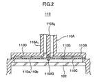
- Fig. 2 is a partially expanded view of the radial line slot antenna 110 of the plasma processing apparatus 100 showed in Fig. 1.
- the coaxial waveguide 110A has a center conductor 110A 2 in an external waveguide 110A 1 connected to the antenna body 110B.
- the center conductor 110A 2 is connected to the slot plate 110C via an opening formed in the retardation plate 110D.
- the slot plate 110C is fixed to the center conductor 110A 2 by a screw 110A 3 .
- the top of the screw 110A 3 protrudes from the slot plate 110C.
- a clearance 110G of 6 mm height is provided between the slot plate 110C and the cover plate 102 so as to store the top of the screw 110A 3 .
- the construction showed in Figs. 1 and 2 causes a problem such that the heat transferred from the high density plasma formed in the processing chamber 101 easily accumulates in the cover plate 102 and the shower plate 103 because the clearance 110G is formed between the slot plate, that is, the radial line slot antenna 110, and the cover plate 102.
- the heat accumulates, as described above, in the cover plate 102 and the shower plate 103 of the plasma processing apparatus 100 showed in Fig. 1, the temperature of the shower plate 103 increases, which results in the dissociation of certain kinds of plasma gases provided from the supply port 105.
- This problem is serious since the plasma processing apparatus 100 is usually operated with the processing chamber 101 heated up to about 150 degree C so as to avoid the formation of deposits on the inner face of the processing chamber 101.
- the shower plate 103 or the cover plate 102 of thermally conductive materials such as AlN in order to avoid heat buildup in the shower plate 103 or the cover plate 102, the alternative material increases dielectric loss, which results in difficulties in forming microwave plasma.
- Another and more specific object of the present invention is to provide a plasma processing apparatus in which the abnormal discharge on the face of the radial line slot antenna is eliminated, and additionally, the efficiency of heat dissipation is improved.
- Yet another object of the present invention is to improve the efficiency of plasma excitation by the microwave antenna of the plasma processing apparatus.
- the present invention achieves one or more of the above objects by providing a plasma processing apparatus, comprising a processing vessel defined by an outer wall and having a stage for holding a substrate to be processed, an evacuation system coupled to said processing vessel, a plasma gas supplying part for supplying plasma gas to said processing vessel, a microwave antenna provided on said processing vessel in correspondence to said plasma gas supplying part, said microwave antenna being supplied with electric power through a coaxial waveguide, and a microwave power source coupled to said microwave antenna electrically, said microwave antenna being defined by a first outer surface forming a microwave radiation surface and a second outer surface opposing said first outer surface, wherein an outer waveguide constructing said coaxial waveguide is coupled to said second outer surface, and a center conductor constructing said coaxial waveguide, a point part of which is separated from said first outer surface, forms capacitive coupling with said first outer surface.
- the center conductor of the coaxial waveguide supplying microwave electric power to the radial line slot antenna is not coupled directly to the conductive slot plate forming the radiation surface of the radial line slot antenna, and consequently, the conductive slot plate does not need to be fixed to the center conductor by a screw.
- problems such as the concentration of electric field and associated abnormal discharge caused by the protrusion of the top of the screw are eliminated.
- the plasma processing can be performed stably without damaging the antenna.
- the conductive slot plate does not need to be fixed to the center conductor by the screw, no room to store the protruding top of the screw is required between the conductive slot plate and the outer wall of the processing vessel. It is possible to place the conductive slot plate in intimate contact with the microwave transparent window formed on the outer wall of the processing vessel. As a result, the microwave transparent window can be cooled by cooling the antenna so that it is possible to make the microwave transparent window and/or the shower plate to supply plasma gas, of Al2O3 that has not been used conventionally because its dielectric loss is small but thermal conductivity is too low.
- the retardation plate provided between the first surface and the second surface of the antenna can be made of Al2O3, SiO2, and SiN of low dielectric loss instead of conventionally used AlN of high dielectric loss.
- a shower plate made of a dielectric material of low dielectric loss, having a plasma gas passage and a plurality of apertures communicating to the plasma gas passage is used as the plasma gas supplying part to provide uniform plasma gas.
- the plasma gas can be provided through a tube provided on the outer wall of the processing vessel. In the latter case, the construction becomes simpler, and the cost incurred in manufacturing the plasma processing apparatus may be greatly reduced.
- the impedance change between the center conductor and the slot plate is optimized by separating the point part of the center conductor from the slot plate by about 3.8 mm, which minimizes the reflection of microwaves due to capacitive coupling.
- the taper structure formed at the point part of the center conductor optimizes the impedance change between the center conductor and the slot plate.
- the microwave antenna can be provided so that the slot plate is exposed to the aperture formed on the outer wall of the processing vessel.
- the processing vessel is efficiently sealed by sealing only the peripheral part of the antenna with sealing material.
- the microwave is not attenuated by a microwave transparent window, for example, and consequently, the microwave plasma is efficiently excited.
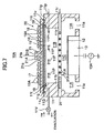
- FIGS.3A and 3B are diagrams showing the construction of a microwave plasma processing apparatus 10 according to a first embodiment of the present invention.
- the microwave plasma processing apparatus 10 includes a processing vessel 11 and a stage 13 provided in the processing vessel 11 for holding a substrate 12 to be processed by an electrostatic chuck, wherein the stage 13 is preferably formed of AlN or Al 2 O 3 by a hot isostatic pressing (HIP) process.
- the processing vessel 11 there are formed two or three evacuation ports 11a in a space 11A surrounding the stage 13 with an equal distance, and hence with an axial symmetry with respect to the substrate 12 on the stage 13.
- the processing vessel 11 is evacuated to a low pressure via the evacuation port 11a by a gradational lead screw pump.
- the processing vessel 11 is preferably formed of an austenite stainless steel containing Al, and there is formed a protective film of aluminum oxide on the inner wall surface by an oxidizing process. Further, there is formed a disk-shaped shower plate 14 of dense Al 2 O 3 , formed by a HIP process, in the part of the outer wall of the processing vessel 11 corresponding to the substrate 12 as a part of the outer wall, wherein the shower plate 14 includes a large number of nozzle apertures 14A.
- the Al 2 O 3 shower plate 14 thus formed by a HIP process is formed by using an Y 2 O 3 additive and has porosity of 0.03% or less. This means that the Al 2 O 3 shower plate is substantially free from pores or pinholes and has a very large, while not so large as that of AlN, thermal conductivity for a ceramic of 30W/m ⁇ K.
- the shower plate 14 is mounted on the processing vessel 11 via a seal ring 11s, and a cover plate 15 of dense Al 2 O 3 formed also of an HIP process is provided on the shower plate 14 via a seal ring 11t.
- the shower plate 14 is formed with a depression 14B communicating with each of the nozzle apertures 14A and serving for the plasma gas passage, at the side thereof contacting with the cover plate 15, wherein the depression 14B also communicates with another plasma gas passage 14C formed in the interior of the shower plate 14 in communication with a plasma gas inlet 11p formed on the outer wall of the processing vessel 11.
- the shower plate 14 is held by an extending part 11b formed on the inner wall of the processing vessel 11, wherein the extending part 11b is formed with a round surface at the part holding the shower plate 14 so as to suppress electric discharge.
- the plasma gas such as Ar or Kr supplied to the plasma gas inlet 11p is supplied to a space 11B right underneath the shower plate 14 uniformly via the apertures 14A after being passed through the passages 14C and the depression 14B in the shower plate 14.
- a radial line slot antenna 20 formed of a disk-shaped slot plate 16 formed with a number of slots 16a and 16b shown in FIG.3B in intimate contact with the cover plate 15, a disk-shaped antenna body 17 holding the slot plate 16, and a retardation plate 18 of a dielectric material of low loss such as Al 2 O 3 , SiO 2 or Si 3 N 4 sandwiched between the slot plate 16 and the antenna body 17.
- the radial line slot antenna 20 is mounted on the processing vessel 11 by way of a seal ring 11u, and a microwave of 2.45GHz or 8.3 GHz frequency is fed to the radial line slot antenna 20 from an external microwave source (not shown) via a coaxial waveguide 21.
- the microwave thus supplied is radiated into the interior of the processing vessel from the slots 16a and 16b on the slot plate 16 via the cover plate 15 and the shower plate 14.
- the microwaves cause excitation of plasma in the plasma gas supplied from the apertures 14A in the space 11B right underneath the shower plate 14.
- the cover plate 15 and the shower plate 14 are formed of Al 2 O 3 and function as an efficient microwave-transmitting window.
- the plasma gas is held at the pressure of about 6666Pa - 13332Pa (about 50 - 100Torr) in the foregoing passages 14A - 14C.
- the microwave plasma processing apparatus 10 of the present embodiment has a ring-shaped groove 11g on a part of the processing vessel 11 so as to engage with the slot plate 16.
- the pressure in the gap formed between the slot plate 16 and the cover plate 15 is reduced and the radial line slot antenna 20 is urged firmly upon the cover plate 15 by the atmospheric pressure.
- a gap includes not only the slots 16a and 16b formed in the slot plate 16 but also a gap formed for various other reasons. It should be noted further that such a gap is sealed by the seal ring 11u provided between the radial line slot antenna 20 and the processing vessel 11.
- an outer waveguide tube 21A of the coaxial waveguide 21A is connected to the disk-shaped antenna body 17 while the point part 21b of a center conductor 21B is connected to the slot plate 16 via an opening formed in the retardation plate 18. That is, the point part 21b is preferably formed at a distance of more than 1 mm, more preferably, 3.8 mm from the slot plate 16.
- the microwave fed to the coaxial waveguide 21A is propagated in the outer radial directions between the antenna body 17 and the slot plate 16 and is emitted from the slots 16a and 16b. If the distance between the retardation plate 18 and the slot plate 16, that is, the thickness of the retardation plate 18, is less than 1 mm, the risk of breakdown increases (becomes not negligible). In the case of 2.45 GHz microwave, the maximum efficiency of supplying power is achieved with the distance between the point part 21b and the slot plate 16 being about 3.8 mm.
- a taper unit 21a is formed correspondingly to the taper unit 21b of the center conductor 21B at the point part of the outer waveguide tube 21A, that is, the joint between the outer waveguide tube 21A and the antenna body 17.
- FIG.3B shows the slots 16a and 16b formed on the slot plate 16.
- the slots 16a are arranged in a concentric manner such that there is provided a slot 16b for each slot 16a such that the slot 16b crosses the slot 16a perpendicularly and such that the slot 16b is aligned concentrically with the slot 16a.
- the slots 16a and 16b are formed with an interval corresponding to the wavelength of the microwave compressed by the radiation plate 16 in the radial direction of the slot plate 16, and as a result, the microwave is radiated from the slot plate 16 in the form of a near plane wave. Because the slots 16a and the slots 16b are formed in a mutually perpendicular relationship, the microwave thus radiated forms a circularly polarized wave including two perpendicular polarization components.
- a cooling block 19 formed with a cooling water passage 19A on the antenna body 17, and the heat accumulated in the shower plate 14 is absorbed via the radial line slot antenna 20 by cooling the cooling block 19 with cooling water in the cooling water passage 19A.
- the cooling water passage 19A is formed on the cooling block 19 in a spiral form, and cooling water having a controlled oxidation-reduction potential is supplied thereto, wherein the control of the oxidation reduction potential is achieved by eliminating oxygen dissolved in the cooling water by way of bubbling of an H 2 gas.
- desired uniform substrate processing is achieved in a space 11C between the process gas supply structure 31 and the substrate 12.
- Such substrate processing includes plasma oxidation processing, plasma nitridation processing, plasma oxynitridation processing, and plasma CVD processing.
- a reactive ion etching of the substrate 12 by supplying a readily decomposing fluorocarbon gas such as C 4 F 8 , C 5 F 8 or C 4 F 6 or an etching gas containing F or Cl from the process gas supply structure to the space 11C and further by applying a high-frequency voltage to the stage 13 from a high-frequency power source 13A.
- a readily decomposing fluorocarbon gas such as C 4 F 8 , C 5 F 8 or C 4 F 6 or an etching gas containing F or Cl
- the microwave plasma processing apparatus 10 of the present embodiment it is possible to avoid deposition of reaction byproducts on the inner wall of the processing vessel by heating the outer wall of the processing vessel 11 to a temperature of about 150°C. Thereby, the microwave plasma processing apparatus 10 can be operated constantly and with reliability, by merely conducing a dry cleaning process once a day or so.
- the taper unit 21b of the center conductor 21B is formed at the joint/power supplying unit that connects the center conductor 21B to the taper unit 21b, and the corresponding taper unit 21a in the outer waveguide tube 21A.
- the rapid change in impedance caused by the joint/power supply unit is smoothed, which results in a reflective wave caused by the rapid change in impedance being greatly reduced.
- FIG. 4 is a bottom view showing the construction of the process gas supply structure 31 of FIG.3A.
- the process gas supply structure 31 is formed by a conductive body such as an Al alloy containing Mg or a stainless steel added with Al and the lattice shaped gas passage 31A is connected to the process gas inlet port 11r at a process gas supply port 31R and releases the process gas uniformly into the foregoing space 11C from the process gas nozzle apertures 31B formed at the bottom surface. Further, there are formed openings 31C in the process gas supply structure 31 between the adjacent process gas passages 31A for passing the plasma or the process gas contained in the plasma therethrough. In the case wherein the process gas supply structure 31 is formed of an Al alloy containing Mg, it is preferable to form a fluoride film on the surface thereof.
- the process gas supplying structure 31 is formed of a stainless steel added with Al, it is preferable to form a passivation film of aluminum oxide on the surface thereof.
- the energy of incident plasma is low because of the low electron temperature of the excited plasma, and the problem of metal contamination of the substrate 12 by the sputtering of the process gas supply structure 31 is avoided.
- the lattice shaped process gas passages 31A and the process gas nozzle apertures 31B are formed so as to encompass an area slightly larger than the substrate 12 represented in FIG.4 by a broken line.
- the process gas supply structure 31 can form a shunting plane of the microwaves by setting the interval between the lattice shaped process gas passages 31A shorter than the microwave wavelength.
- the microwave excitation of plasma takes place only in the space 11B, and there occurs excitation of the process gas in the space 11C including the surface of the substrate 12 by the plasma that has caused diffusion from the excitation space 11B.
- such a construction can prevent the substrate from being exposed directly to the microwave at the time of ignition of the plasma, and thus, damaging of the substrate by the microwave is avoided.
- the supply of the process gas is controlled uniformly by the process gas supply structure 31, and the problem of excessive dissociation of the process gas on the surface of the substrate 12 is eliminated.
- the microwave plasma processing apparatus 10 is effective for fabricating various semiconductor devices of different generations characterized by different design rules.
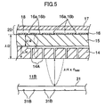
- FIG.5 is a diagram showing a part of the plasma processing apparatus 10 of FIG.3A including the shower plate 14, the cover plate 15 and the radial line slot antenna 20.
- the distance between the bottom surface of the shower plate 14 and the process gas supplying structure 31 is set to be equal to an integer multiple of the quarter wavelength of the microwave for efficient excitation of plasma in the region right underneath the shower plate 14.
- the node of the microwave emitted from the radial line slot antenna 20 be located coincident to the slots 16a and 16b. Further, it is preferable that the node be located also coincident to the bottom surface of the shower plate 14 for avoiding the electric discharge in the shower nozzle apertures 14A. Because of this reason, it is preferable to set the total thickness of the shower plate 14 and the cover plate 15 to be equal to one-half the wavelength of the microwave.
- each the shower plate 14 and the cover plate 15 By setting the thickness of each the shower plate 14 and the cover plate 15 to be equal to a quarter wavelength of the microwave, in particular, the node of the microwave is located in the vicinity of the interface between the shower plate 14 and the cover plate 15, and the electric discharge in the plasma gas passage 14B, which is formed along this interface, is effectively suppressed.
- FIG.6 shows the schematic construction of the microwave source connected to the coaxial waveguide 21 of FIG. 2A.
- the coaxial waveguide is connected to an edge of the waveguide extending from an oscillation part 25 including therein a magnetron 25A oscillating at the frequency of 2.45GHz or 8.3GHz via an isolator 24, a power monitor 23 and a tuner 22 in this order.
- the microwave formed by the oscillator 25 is supplied to the radial line slot antenna 20, and the microwave reflected back from the high-density plasma formed in the plasma processing apparatus 10 is returned again to the radial line slot antenna 20 after conducting an impedance adjustment by the tuner 22.
- the isolator 24 is an element having directivity and functions so as to protect the magnetron 25A in the oscillation part 25 from the reflection wave.
- the rapid change in impedance caused by the joint is reduced by forming the taper units 21At and 21Bt at the joint, or the power supplying unit, between the coaxial waveguide 21 and the radial line slot antenna 20.
- the reflection of microwaves caused by the rapid change in impedance is suppressed, which makes the supplying of microwaves from the coaxial waveguide 21 to the antenna 20 stable.
- the microwave plasma processing apparatus 10 As showed in a variation showed in Fig. 8, it is possible to replace the taper faces 21At and 21Bt with round faces 21Ar and 21Br, respectively.
- the change in impedance caused by the joint is further reduced by forming the round faces, which results in further efficient suppressing of the reflective wave.
- the distance between the shower plate 14 exposed to the heat caused by the plasma and the cooing part is reduced substantially as compared with the conventional microwave plasma processing apparatus of FIGS.1A and 1B, and as a result, it becomes possible to use a material such as Al 2 O 3 having a small dielectric loss and also a small thermal conductivity for the microwave transmission window in place of AlN, which is characterized by large dielectric loss. Thereby, the efficiency of plasma processing and hence the processing rate are improved while simultaneously suppressing the temperature rise of the shower plate.
- the gas including the reaction byproduct formed in the space 11C as a result of the substrate processing forms a stable gas flow to the space 11A at the outer surrounding area because of the reduced distance between the shower plate 14 and the substrate 12 facing the shower plate 14, and the byproduct is removed from the space 11C quickly.
- the temperature of the outer wall of the processing vessel 11 to be about 150°C, it becomes possible to eliminate the deposition of the reaction byproduct on the inner wall of the processing vessel 11 substantially completely, and the processing apparatus 10 becomes ready for the next process quickly.
- Fig. 7 is a diagram showing the construction of a plasma processing apparatus 10A according to a second embodiment of the present invention.
- the parts described earlier are referred to by the same reference numerals, and their description is omitted.
- the plasma processing apparatus 10A has a construction similar to the plasma processing apparatus 10 showed in Figs. 3A and 3B. They are different, however, in that the shower plate 14 is removed, and the gas inlets 11P protrude from the gas inlet ports 11p in the space 11B of the processing vessel.
- This construction can form high density plasma in the space 11B by exciting the plasma gas supplied through the gas inlets 11P by the microwave supplied by the radial line slot antenna 20.
- the high density plasma thus formed is less uniform than the high density plasma obtained using the shower plate 14, but the construction of the plasma processing apparatus 10A is much simpler than that of the foregoing plasma processing apparatus 10.
- the heat flow entering to the cover plate 15 is absorbed by the cooling unit 17 via the radial line slot antenna 20.
- plural inlets 11P be provided at symmetrical positions around the substrate in order to form plasma as uniform as possible.
- the protrusion of the top of screw from the face of the slot plate 16 can be avoided by forming the point part 21b of the center conductor 21B of the coaxial waveguide at a distance from the slot plate 16 to form capacitive coupling between the two. It is possible to couple the antenna 20 so that the slot plate 16 coheres with the cover plate 15.
- Fig. 8 is a diagram showing the construction of a microwave plasma processing apparatus 10B according to a third embodiment of the present invention.
- parts that have been previously described are referred to by the same numerals, and their description will be omitted.
- the construction of the microwave plasma processing apparatus 10B is similar to that of the microwave plasma apparatus processing 10 described previously.
- the microwave plasma processing apparatus 10B is different, however, in that the process gas supply structure 31 is removed. Additionally, the lower face of the extending part 11b of the processing vessel 11 is round so as to avoid abnormal discharge.
- the construction of the plasma processing apparatus 10B prevents problems of the plasma forming just under the shower plate 14 reflecting the microwaves so that the microwaves reach the surface of the substrate 12, and the plasma being excited in the region near the surface. It is possible to prevent the microwave from reaching, and damaging, the substrate at the ignition of the plasma by setting the pressure in the processing vessel temporarily at a high level, 133 Pa (about 1 Torr), for example, to make sure that the plasma is ignited. The pressure in the processing vessel is soon adjusted to the process pressure, 13.3 Pa (about 0.1 Torr), for example, after the ignition of the plasma.
- the plasma processing apparatus 10B because the process gas supply structure 30 is removed, the process gas needs to be supplied from the plasma gas supply port 11p with the plasma gas. Accordingly, the plasma processing apparatus 10B can perform oxidation processing, nitridation processing, oxynitridation processing, and so forth on the surface of the substrate 12.
- the protrusion of the top of screw from the face of the slot plate 16 can be avoided by forming the point part 21b of the center conductor 21B of the coaxial waveguide at a distance from the slot plate 16 to form capacitive coupling between the two. It is possible to couple the antenna 20 so that the slot plate 16 coheres with the cover plate 15.
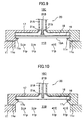
- Fig. 9 is a diagram showing a plasma processing apparatus 10C according to a fourth embodiment of the present invention.
- parts that have been previously described are referred to by the same numerals, and their description will be omitted.
- the cover plate 15 is formed as the part of the microwave antenna 20, instead of the part of the processing vessel 11.
- the antenna body 17 is assembled to the processing vessel 11 via the seal ring 11u.
- the cover plate 15 that is formed as the part of the outer wall of the processing vessel 11 is removed, and a dielectric plate 15A covering the slot plate 16 is provided as a monolith on the antenna 17 instead.
- the dielectric plate 15A coheres with the slot plate 16, whereas the slot plate 16 is supported by the antenna body 17 via the retardation plate 18.
- the antenna 20 when the processing vessel 11 is evacuated, the antenna 20 is put under great atmospheric pressure. In the present embodiment, however, the antenna body 17 can absorb the tension caused by the atmospheric pressure. The thickness of the dielectric plate 15A is consequently reduced. As a result, the loss of microwaves caused by the dielectric plate 15A is reduced, and the excitation efficiency of the high density plasma in the space 11B of the processing vessel 11 is improved.
- the shower plate 14 is not provided, and the plasma gas is supplied through the inlets 11P. It is possible to provide the plasma processing apparatus 10C with the shower plate 14.
- Fig. 10 is a diagram showing the construction of a plasma processing apparatus 10D according a fifth embodiment of the present invention.
- the parts described previously are referred to by the same reference numerals, and their description is omitted.
- the dielectric plate 15A provided in the construction of the embodiment of Fig. 9 is omitted, and the slot plate 16 is exposed in the processing vessel 11.
- the microwave is provided directly from the slot plate 16 to the inner space 11B of the processing vessel 11, not through the dielectric plate 15A or the cover plate 15. It is possible to efficiently excite the microwave plasma in the inner space 11B.
- the seal ring 17u does not suffer much damage since it is formed in the peripheral portion of the antenna body 17.
- the plasma processing apparatus 10D can perform stable plasma processing by cooling the antenna body 17 as in the embodiment of Figs. 3A and 3B.
- the antenna 20 when the processing vessel 11 is evacuated, the antenna 20 is put under great atmospheric pressure. In the present embodiment, however, the antenna body 17 can absorb the tension caused by the atmospheric pressure without mechanically damaging the retardation plate 18.
- the protrusion of the top of screw from the face of the slot plate can be avoided by providing the center conductor of the coaxial waveguide that supplies microwaves to the radial line slot antenna so that the point part of the center conductor is separated from the slot plate constructing the radial line slot antenna.
- the slot plate can cohere with a corresponding microwave transparent window. Thanks to the construction, abnormal discharge can be avoided, and the microwave transparent window can be efficiently cooled via the radial line slot antenna.
- the radial line slot antenna and the dielectric plate constructing the microwave transparent window can be monolithic by the present invention, and consequently, the excitation efficiency of the microwave plasma is improved.
- the radial line slot antenna is directly attachable to the processing vessel. Accordingly, the microwave is supplied directly to the processing vessel, not through the microwave transparent window, and the excitation efficiency of the microwave plasma is further improved.
Landscapes
- Physics & Mathematics (AREA)
- Engineering & Computer Science (AREA)
- Plasma & Fusion (AREA)
- Chemical & Material Sciences (AREA)
- Analytical Chemistry (AREA)
- Plasma Technology (AREA)
- Drying Of Semiconductors (AREA)
- Chemical Vapour Deposition (AREA)
- ing And Chemical Polishing (AREA)
Abstract
Description
a processing vessel defined by an outer wall and having a stage for holding a substrate to be processed,
an evacuation system coupled to said processing vessel,
a plasma gas supplying part for supplying plasma gas to said processing vessel,
a microwave antenna provided on said processing vessel in correspondence to said plasma gas supplying part, said microwave antenna being supplied with electric power through a coaxial waveguide, and
a microwave power source coupled to said microwave antenna electrically, said microwave antenna being defined by a first outer surface forming a microwave radiation surface and a second outer surface opposing said first outer surface,
wherein
an outer waveguide constructing said coaxial waveguide is coupled to said second outer surface, and
a center conductor constructing said coaxial waveguide, a point part of which is separated from said first outer surface, forms capacitive coupling with said first outer surface.
Claims (14)
- A plasma processing apparatus, comprising:a processing vessel defined by an outer wall and having a stage for holding a substrate to be processed;an evacuation system coupled to said processing vessel;a plasma gas supplying part for supplying plasma gas to said processing vessel;a microwave antenna provided on said processing vessel in correspondence to said plasma gas supplying part, said microwave antenna being supplied with electric power through a coaxial waveguide; anda microwave power source coupled to said microwave antenna electrically, said microwave antenna being defined by a first outer surface forming a microwave radiation surface and a second outer surface opposing said first outer surface;whereinan outer waveguide constructing said coaxial waveguide is coupled to said second outer surface; anda center conductor constructing said coaxial waveguide, a point part of which is separated from said first outer surface, forms capacitive coupling with said first outer surface.
- The microwave plasma processing apparatus as claimed in claim 1, wherein, in said micro wave antenna,
a dielectric film is provided between said first outer surface and said second outer surface; and
said point part of said center conductor forms capacitive coupling with said first outer surface via said dielectric film. - The microwave plasma processing apparatus as claimed in claim 1, wherein said point part is separated from said first outer surface by about 3.8 mm.
- The microwave plasma processing apparatus as claimed in claim 1, wherein said dielectric film is selected from SiO2, Al2O3, and Si3N4.
- The microwave plasma processing apparatus as claimed in claim 1, wherein
said processing vessel is provided, on said outer wall, with a microwave transparent window opposing said substrate on said stage; and
said microwave antenna is coupled to said microwave transparent window. - The microwave plasma processing apparatus as claimed in claim 5, wherein said microwave antenna is provided so that said first outer surface is in intimate contact with said microwave transparent window.
- The microwave plasma processing apparatus as claimed in claim 1, wherein
an opening is formed on said outer wall of said processing vessel in correspondence with said substrate on said stage; and
said microwave antenna is provided so that said first outer surface opposes said substrate through said opening. - The microwave plasma processing apparatus as claimed in claim 7, wherein said first outer surface is made of aluminum or silicon.
- The microwave plasma processing apparatus as claimed in claim 1, said point part of said center conductor forms a tapered part in which the diameter increases toward said first outer surface.
- The microwave plasma processing apparatus as claimed in claim 1, wherein said plasma gas supplying part is provided opposing to said substrate and further comprises a dielectric plate on which a plasma gas passage that can communicate to said plasma gas supplying part and a plurality of aperture forming parts communicating thereto are formed.
- The microwave plasma processing apparatus as claimed in claim 1, wherein said plasma gas supplying part is constructed by a plurality of tubes formed in said outer wall of said processing vessel that can communicate with a plasma gas source.
- The microwave plasma processing apparatus as claimed in claim 1, further comprising:a processing gas supplying part provided between said plasma gas supplying part and said substrate.
- The microwave plasma processing apparatus as claimed in claim 12, wherein said processing gas supplying part is provided with a processing gas passage that can communicate with a processing gas source, a first aperture through which plasma flows, and a plurality of second apertures communicating with said processing gas passage.
- The microwave plasma processing apparatus as claimed in claim 12, further comprising a high frequency power supply coupled to said stage.
Applications Claiming Priority (3)
| Application Number | Priority Date | Filing Date | Title |
|---|---|---|---|
| JP2001094274 | 2001-03-28 | ||
| JP2001094274A JP2002299331A (en) | 2001-03-28 | 2001-03-28 | Plasma processing equipment |
| PCT/JP2002/003107 WO2002080248A1 (en) | 2001-03-28 | 2002-03-28 | Plasma processing device |
Publications (2)
| Publication Number | Publication Date |
|---|---|
| EP1300875A1 true EP1300875A1 (en) | 2003-04-09 |
| EP1300875A4 EP1300875A4 (en) | 2006-12-20 |
Family
ID=18948499
Family Applications (1)
| Application Number | Title | Priority Date | Filing Date |
|---|---|---|---|
| EP02707228A Withdrawn EP1300875A4 (en) | 2001-03-28 | 2002-03-28 | PLASMA TREATMENT DEVICE |
Country Status (7)
| Country | Link |
|---|---|
| US (1) | US20030148623A1 (en) |
| EP (1) | EP1300875A4 (en) |
| JP (1) | JP2002299331A (en) |
| KR (1) | KR100501777B1 (en) |
| CN (1) | CN1210768C (en) |
| IL (1) | IL153153A (en) |
| WO (1) | WO2002080248A1 (en) |
Cited By (1)
| Publication number | Priority date | Publication date | Assignee | Title |
|---|---|---|---|---|
| EP1672093B1 (en) * | 2003-09-17 | 2013-07-10 | Tokyo Electron Limited | Film-forming apparatus and film-forming method |
Families Citing this family (22)
| Publication number | Priority date | Publication date | Assignee | Title |
|---|---|---|---|---|
| JP2004296512A (en) * | 2003-03-25 | 2004-10-21 | Tokyo Electron Ltd | Cleaning method for plasma processing apparatus |
| JP3974553B2 (en) * | 2003-05-07 | 2007-09-12 | 東京エレクトロン株式会社 | Plasma processing apparatus, antenna for plasma processing apparatus, and plasma processing method |
| JP2005093737A (en) * | 2003-09-17 | 2005-04-07 | Tadahiro Omi | Plasma film forming apparatus, plasma film forming method, semiconductor device manufacturing method, liquid crystal display device manufacturing method, and organic EL element manufacturing method |
| JP4532897B2 (en) * | 2003-12-26 | 2010-08-25 | 財団法人国際科学振興財団 | Plasma processing apparatus, plasma processing method and product manufacturing method |
| CN101218376A (en) | 2005-06-17 | 2008-07-09 | 国立大学法人东北大学 | Protective film structure for metal member, and metal component, semiconductor or flat panel display manufacturing apparatus using the same |
| CN101198726B (en) | 2005-06-17 | 2011-07-27 | 国立大学法人东北大学 | Metal oxide film, laminated body, metal member and manufacturing method thereof |
| JP4620537B2 (en) * | 2005-07-21 | 2011-01-26 | 東京エレクトロン株式会社 | Plasma processing apparatus and plasma processing apparatus control method |
| EP1956645A4 (en) * | 2005-11-08 | 2010-04-28 | Univ Tohoku | ASPERSION PLATE AND PLASMA PROCESSING APPARATUS USING THE ASPERSION PLATE |
| JP5082229B2 (en) * | 2005-11-29 | 2012-11-28 | 東京エレクトロン株式会社 | Plasma processing equipment |
| JP5121698B2 (en) * | 2006-03-06 | 2013-01-16 | 東京エレクトロン株式会社 | Plasma processing equipment |
| JP5229847B2 (en) * | 2006-03-31 | 2013-07-03 | 国立大学法人東北大学 | Porous member, method for manufacturing the same, and method for manufacturing ceramic member using the method |
| CN101855946B (en) * | 2007-10-04 | 2013-02-13 | 东京毅力科创株式会社 | Plasma processing apparatus and method for adjusting plasma density distribution |
| JP5396745B2 (en) * | 2008-05-23 | 2014-01-22 | 東京エレクトロン株式会社 | Plasma processing equipment |
| JP5297885B2 (en) * | 2008-06-18 | 2013-09-25 | 東京エレクトロン株式会社 | Microwave plasma processing equipment |
| WO2011125703A1 (en) * | 2010-03-31 | 2011-10-13 | 東京エレクトロン株式会社 | Plasma nitridization method |
| TWI559819B (en) * | 2010-09-10 | 2016-11-21 | Emd Corp | Plasma processing device |
| JP6338462B2 (en) * | 2013-09-11 | 2018-06-06 | 東京エレクトロン株式会社 | Plasma processing equipment |
| CN112366128B (en) | 2014-04-09 | 2024-03-08 | 应用材料公司 | Flow modules for providing symmetrical flow paths in processing chambers |
| EP3813092A1 (en) * | 2019-10-23 | 2021-04-28 | EMD Corporation | Plasma source |
| JP7753351B2 (en) * | 2020-09-21 | 2025-10-14 | ラム リサーチ コーポレーション | Carrier ring for suspending the gas plate in the TCP chamber |
| US20220415617A1 (en) * | 2021-06-25 | 2022-12-29 | Applied Materials, Inc. | Remote plasma apparatus for generating high-power density microwave plasma |
| KR20250003043A (en) | 2023-06-30 | 2025-01-07 | 세메스 주식회사 | Antenna unit and substrate treating apparatus including the same |
Family Cites Families (6)
| Publication number | Priority date | Publication date | Assignee | Title |
|---|---|---|---|---|
| TW293983B (en) * | 1993-12-17 | 1996-12-21 | Tokyo Electron Co Ltd | |
| US5698036A (en) * | 1995-05-26 | 1997-12-16 | Tokyo Electron Limited | Plasma processing apparatus |
| JPH0963793A (en) * | 1995-08-25 | 1997-03-07 | Tokyo Electron Ltd | Plasma processing device |
| JP3430053B2 (en) * | 1999-02-01 | 2003-07-28 | 東京エレクトロン株式会社 | Plasma processing equipment |
| KR100745495B1 (en) * | 1999-03-10 | 2007-08-03 | 동경 엘렉트론 주식회사 | Semiconductor manufacturing method and semiconductor manufacturing apparatus |
| EP1879213B1 (en) * | 1999-05-26 | 2012-03-14 | Tokyo Electron Limited | Plasma processing apparatus |
-
2001
- 2001-03-28 JP JP2001094274A patent/JP2002299331A/en not_active Withdrawn
-
2002
- 2002-03-28 KR KR10-2002-7015999A patent/KR100501777B1/en not_active Expired - Fee Related
- 2002-03-28 EP EP02707228A patent/EP1300875A4/en not_active Withdrawn
- 2002-03-28 CN CNB028009207A patent/CN1210768C/en not_active Expired - Fee Related
- 2002-03-28 WO PCT/JP2002/003107 patent/WO2002080248A1/en not_active Ceased
- 2002-03-28 US US10/296,857 patent/US20030148623A1/en not_active Abandoned
- 2002-03-28 IL IL153153A patent/IL153153A/en not_active IP Right Cessation
Cited By (1)
| Publication number | Priority date | Publication date | Assignee | Title |
|---|---|---|---|---|
| EP1672093B1 (en) * | 2003-09-17 | 2013-07-10 | Tokyo Electron Limited | Film-forming apparatus and film-forming method |
Also Published As
| Publication number | Publication date |
|---|---|
| US20030148623A1 (en) | 2003-08-07 |
| EP1300875A4 (en) | 2006-12-20 |
| IL153153A0 (en) | 2003-06-24 |
| IL153153A (en) | 2007-05-15 |
| WO2002080248A1 (en) | 2002-10-10 |
| CN1210768C (en) | 2005-07-13 |
| KR100501777B1 (en) | 2005-07-20 |
| KR20030004426A (en) | 2003-01-14 |
| CN1460287A (en) | 2003-12-03 |
| JP2002299331A (en) | 2002-10-11 |
Similar Documents
| Publication | Publication Date | Title |
|---|---|---|
| EP1376669B1 (en) | Plasma processing device | |
| US7115184B2 (en) | Plasma processing device | |
| US7097735B2 (en) | Plasma processing device | |
| US20030148623A1 (en) | Plasma processing device | |
| KR100685248B1 (en) | Plasma processing equipment | |
| US20090229755A1 (en) | Plasma processing apparatus | |
| JP4113895B2 (en) | Plasma processing equipment | |
| JP4113896B2 (en) | Plasma processing equipment |
Legal Events
| Date | Code | Title | Description |
|---|---|---|---|
| PUAI | Public reference made under article 153(3) epc to a published international application that has entered the european phase |
Free format text: ORIGINAL CODE: 0009012 |
|
| 17P | Request for examination filed |
Effective date: 20021128 |
|
| AK | Designated contracting states |
Kind code of ref document: A1 Designated state(s): AT BE CH CY DE DK ES FI FR GB GR IE IT LI LU MC NL PT SE TR Designated state(s): AT BE CH CY DE DK ES FI FR GB GR IE IT LI LU MC NL PT SE TR |
|
| AX | Request for extension of the european patent |
Extension state: AL LT LV MK RO SI |
|
| A4 | Supplementary search report drawn up and despatched |
Effective date: 20061116 |
|
| RIC1 | Information provided on ipc code assigned before grant |
Ipc: H05H 1/46 20060101ALI20061110BHEP Ipc: C30B 25/10 20060101ALI20061110BHEP Ipc: C23C 16/50 20060101ALI20061110BHEP Ipc: H01J 37/32 20060101AFI20061110BHEP |
|
| 17Q | First examination report despatched |
Effective date: 20070525 |
|
| GRAP | Despatch of communication of intention to grant a patent |
Free format text: ORIGINAL CODE: EPIDOSNIGR1 |
|
| GRAC | Information related to communication of intention to grant a patent modified |
Free format text: ORIGINAL CODE: EPIDOSCIGR1 |
|
| RIN1 | Information on inventor provided before grant (corrected) |
Inventor name: HONGOH, TOSHIAKI,TOKYO ELECTRON LIMITED Inventor name: GOTO,T,C Inventor name: SUGAWA, SHIGETOSHI,TOHOKU UNIVERSITY Inventor name: HIRAYAMA, MASAKIC Inventor name: OHMI, TADAHIRO |
|
| STAA | Information on the status of an ep patent application or granted ep patent |
Free format text: STATUS: THE APPLICATION IS DEEMED TO BE WITHDRAWN |
|
| 18D | Application deemed to be withdrawn |
Effective date: 20090730 |