FIELD OF THE INVENTION
The present invention relates to an X-ray
detector for detecting X-ray transmission data for a
plurality of slices at one time and to an X-ray CT
apparatus comprising said detector. More particularly,
it relates to an X-ray detector for performing highly
accurate measurement, while a measurement circuit is
not affected by outputs of photo diode cells that are
not used for measurement when a switch array for
selecting slice thickness is provided near the photo
diode array for converting dose of said transmitted
X-ray into electric signals, and to an X-ray CT
apparatus that can obtain a reconstructed image with
high diagnosability, comprising said X-ray detector.
BACKGROUND OF THE INVENTION
In recent years, the multi-slice X-ray CT
apparatus has been attracting attention. In the X-ray
CT apparatus, plural lines of X-ray detecting element
arrays in the slicing direction are arranged (that is,
the X-ray detecting element arrays are
two-dimensionally arranged), and two-dimensional
X-ray data is collected with one irradiation of X-rays to
improve throughput of the apparatus. (Hereafter, an
X-ray detector used for said multi-slice X-ray CT
apparatus is referred to as a multi-slice X-ray
detector.) Compared with the conventional detector
with a one line array, (Hereafter, such a detector is
referred to as a single-slice X-ray detector and an
X-ray CT apparatus using said single-slice detector is
referred to as a single-slice X-ray CT apparatus), said
multi-slice X-ray CT apparatus has the advantage of
better use efficiency of X-rays radiated from the X-ray
tube. In said multi-slice X-ray detector, a solid-state
detector having scintillators by which high spatial
resolution and high S/N (signal/noise) ratio can be
obtained is used instead of a conventional ionization
chamber type detector using xenon gas. The said
solid-state detector comprises a plurality of X-ray
detecting elements formed from a scintillator for
converting radiated X-rays into light and a light
detecting element such as a silicon photo diode for
detecting the light produced in said scintillator and
outputting it as electric signals, this plurality of said
X-ray detecting elements being arranged in an arc
around an X-ray source both in the channel direction
and in the slicing direction perpendicular to channel
direction. In this manner, a plurality of X-ray
detecting elements is arranged in the channel direction
and in the slicing direction in the multi-slice X-ray
detector. Thus, the number of the output signals of
said multi-slice X-ray detecting elements become much
larger than that of the conventional single-slice X-ray
detector, since a large number of X-ray detecting
elements is arranged in the slicing and channel
directions. It is a pressing object to efficiently
extract said output signals in a limited mounting
space.
As described above, a multiple-element
arrangement is necessary in a detector for an X-ray CT
apparatus. Therefore, not a plurality of separate
channel chips but a light detecting element array in
which a plurality of channels is formed on one chip is
used for the light detecting element for converting the
output light of the scintillator, said light detecting
element array being disclosed in Japanese Patent
Laid-open No. 2000-316841.
As the elements of said light detecting
element array must be densely arranged in a limited
mounting space, semiconductor devices such as a
silicon photo diode are generally used for the light
detecting element. However, although the light
detecting element array used for the conventional
single-slice X-ray detector is constructed with a
one-dimensional array of receivers and output signal
transducers separately only in a single channel
direction, the light detecting element array used for
the multi-slice X-ray detector needs to be constructed
as a two-dimensional array in which the receivers are
separated in the channel direction and in the slicing
direction perpendicular to the channel direction.
Thus, of course, the number of the output
signals per channel increases in accordance with
increase of the number of divisions of the light
detecting element array in the slicing direction.
Further, with a change of slice thickness in the
multi-slice X-ray CT apparatus, the width not only of
X-ray beams to be radiated but also of the X-ray
detecting element in the slicing direction need to be
changed. That is, when examining a lesion with an
X-ray CT apparatus, the optimum slice thickness
depends on the region to be examined, the range of
examination, and the objective disease. Therefore, in
an X-ray CT apparatus, the slice thickness can be
usually selected among several sizes in a range of
around 1-10mm, considering the purpose of
examination. In a conventional single-slice X-ray
detector, the slice thickness for the examination is
changed by changing the width of the X-ray beam to be
radiated. But, in a multi-slice X-ray detector, the slice
thickness of an X-ray beam detected by each X-ray
detecting element line cannot be changed only by
changing the width of an incident X-ray beam. In the
multi-slice X-ray detector, it is necessary not only to
change the width of X-ray beams to be radiated but
also to change the division of the X-ray detecting
element lines in the slicing direction to match the
desired slices thickness.
Therefore, to perform measurement with
several sizes of slice thickness, it is necessary to
change the slice thickness by changing the way in
which the outputs of divided photo diode cells are
combined, since the X-ray detecting elements are
divided among a plurality of photo diode cells as
disclosed in said Japanese Patent Laid-open No.
2000-316841.
Thus, it is necessary that the light detecting
element array used to provide the multi-slice X-ray
detecting elements extensively divided in the slicing
direction, and switch arrays are combined so as to
connect the output of each division to an external
circuit with these divisions combined in the desired
manner. Usually, said switch array is placed near the
light detecting element array, and they are directly
connected with a wire bonding method, as in said
Japanese Patent Laid-open No. 2000-316841. And, the
output signals of the switch array transmitted to the
external circuit from a connector that is mounted on
the substrate and connected to a wiring substrate
using a wire bonding method. The reason for providing
a switching circuit for selecting a slice thickness
before the external circuit, that is, a preamplifier for
amplifying the output of said light detecting element,
is to reduce the total number of said preamplifiers.
The output current of the photo diode
elements comprising each X-ray detecting element of
the X-ray detector constituted as above is converted
into voltage by a current/voltage converter called a
preamplifier.
Fig.7(a) is a basic circuit of said
current/voltage converter, which is comprised of a
photo diode 20 for catching the output light of a
scintillator and converting said light into current, an
amplifier 21 for amplifying current flowing in said
photo diode 20 and a feedback resistor 22 connected
between the minus input terminal and output terminal
of said amplifier 21, parallel to it. The relation between
the input current of said current/voltage converter Ii
(A: ampere), the resistance value of the feedback
resistor 22 Rf (Ω: ohm), and the output voltage Vo (V:
Volt) is indicated with the expression below:
Vo=Rf×Ii
However, there actually exists the internal
resistance 23 in the wiring material used to connect
the photo diode elements and the amplifier 21. Given
that the resistance value of said internal resistance 23
is Ri (Ω: ohm), it works as the input resistance Ri of
said amplifier as shown in Fig.7(b).
Even when said internal resistance Ri exists,
the relation between the input current Ii and the
output voltage Vo is still expressed with the above
expression. But, as shown in Fig7(c), there exists a
condenser C having some parasitic capacitance
between said input resistance Ri and photo diode 20. If
voltage e (that is, voltage that is generated when
current flows in the photo diode 20 due to the light into
which scattered X-rays are converted, or the light
leaking from other scintillators, and said current
charges the photo diode 20 to junction capacitance) is
input through condenser C to amplifier 21
(current/voltage converter), said amplifier works as a
voltage amplifier and the voltage Vo' that is Rf/Ri
times as large as the applied voltage e is output to the
output terminal. As the series internal resistance Ri is
usually several 10mΩ (milliohm) and the feedback
resister Rf is several MΩ (megohm), the amplification
factor of voltage of said amplifier 21 becomes as large
as 106-108 times. Then, even faint voltage causes a
considerable measurement error. More concretely, the
input current of said amplifier is several tens of pA
(picoampere)-1µA(microampere) in normal state and
the output voltage due to said input current is
5V(volt)-10V. But, if there exists said voltage e,
amplifier 21 becomes saturated and its output voltage
becomes close to the source voltage of said amplifier 21
(15V, for example), which appears as a considerable
measurement error. In the X-ray detector for the
multi-slice X-ray CT apparatus, a plurality of photo
diode cells are provided in the slicing direction as
described above. The output of these cells is routed in
a manner appropriate to the slice thickness by
changing the setting of the switches, and then this
output is transmitted to the measuring circuit. Here,
if X-rays enter photo diode cells that are not connected
to the measuring circuit, (Even though central rays do
not enter them since they are narrowed by the
collimator of the radiator in the X-ray tube, some of
the central rays become scattered when the central
rays are transmitted through an object, and said
scattered X-rays enter the photo diode cells that do not
perform measurement.) electric charge generated in
the photo diode cells that are not connected to the
measuring circuit is not discharged outwards, and the
additional voltage is given to the electric load. If the
voltage thus generated in the photo diode cells that do
not perform measurement leaks into a measurement
channel through the parasitic capacitance in the
wiring, the amplification factor of voltage takes large
value as described above, even if the value of said
generated voltage is very small. Thus, said generated
voltage might cause an error so great with regard to the
measured value that it cannot be ignored.
A reconstructed image with high
diagnosability cannot be obtained from the measured
data having such an error. Here, the objects of the
present invention are to provide an X-ray detector for
performing highly accurate measurement, not affected
by output of photo diode cells that are not used for
measurement even when a switch array for selecting
slice thickness is provided near the photo diode array
of a multi-slice X-ray detector for measuring a
plurality of slices at one time, and to provide an X-ray
CT apparatus that can obtain an reconstructed image
with high diagnosability using the data output by said
X-ray detector.
SUMMARY OF THE INVENTION
To achieve the above-mentioned objects, the
present invention provides an X-ray detector
comprising:
wherein said switching circuit routes the
outputs of selected lines of the elements of the light
detecting element array in the slicing direction to an
external circuit, and as well leads the output of lines of
slicing elements that are not used for measurement at
that time to a common ground of said light detecting
element array.
When an X-ray detector is constructed in this
manner, the photo diode cells used for measurement at
the time are not affected by the voltage generated when
output terminals of said photo diode cells which are
not used for measurement are kept open by connecting
output for instance of the photo diode cells used as the
light detecting elements, which are not connected at
the time to an external circuit, to said ground of the
photo diode array. Thus, highly accurate
measurement data can be obtained. Also, in said
switching circuit, all the rows of channels along the
same slicing direction are simultaneously grouped in
accordance with a slice thickness selecting signal
input from an external circuit and output signals from
the cells to said external circuit. Further, said
switching circuit comprises a plurality of
semiconductor switching elements and a switching
element driving signal generating circuit for driving
said switching elements. And,
connection/disconnection of said switching elements
is controlled by said slice thickness selecting signal.
By constructing the switching circuit in this manner,
the structure of the circuit becomes simple, and easy
to connect the output of a cell in a desired position to
the external measuring circuit. Further, cells of said
light detecting element array and said switching
elements are symmetrically arranged. In the cells
that are not separated in the combination made to
match the slice thickness, output signals of the cells
are composed before the cells send said signals to the
switching elements. Further, the switching elements
symmetrically opposite each other operate in the same
way, and are arranged so that the output of each cell is
symmetrically transmitted to the external circuit, for
the purpose of reducing the total number of said
switching elements.
Further, an X-ray CT apparatus of the present
invention comprises:
wherein said X-ray detector comprises;
- a scintillator for generating light as detecting
incident X-rays; and
- an X-ray detecting element array with a
switching circuit, which comprises an light detecting
element array having light-reception area that is
divided in the channel direction and in the slicing
direction, and a switching element array for routing
outputs of said light-reception area that are divided in
the slicing direction and leading these outputs to said
preamplifier, said scintillator and X-ray detecting
element array with a switching circuit being
polygonally arranged on an arcuate line around the
focal point of the X-ray tube both in the slicing
direction and the channel direction with a uniform
angular pitch,
wherein said switching circuit leads the
output of lines of the slicing elements of the light
detecting element array to said preamplifier, said lines
being selected according to the slice thickness signal
set by the scanning condition setting means, and leads
the output of lines of slicing elements that are not used
for measurement to common ground of said light
detecting element array.
In the thus constructed multi-slice X-ray CT
apparatus, photo diodes used as light detecting
elements are arranged in an array shape. Further,
among the switch arrays that are arranged near said
photo diode array for selecting the slice thickness,
output terminals of the switch arrays that are not
connected to the preamplifier are connected to the
ground. Thus, even when electric charge is generated
in a photo diode cell due to incidence of scattered
X-rays, the disturbance voltage can be prevented from
entering the preamplifier that is connected to the
switch arrays. Therefore, it is possible to provide a
multi-slice X-ray CT apparatus for obtaining a
plurality of slice tomograms with high diagnosability,
in which errors of measurement data have been
eliminated.
Also, all the channels of said switching
circuit simultaneously output signals to said
preamplifier after combining rows of cells in the same
slicing direction according to a slice thickness
selecting signal from said scanning condition setting
means.
Also, said switching circuit comprises a
plurality of semiconductor switching elements and a
switching element driving signal generating circuit for
driving said switching elements. And,
connection/disconnection of said switching elements
being controlled by said slice thickness selecting
signal. By constructing the switching circuit in this
manner, it becomes simple, and easy to connect output
of the cells in a desired position to the preamplifier.
Further, cells of said light detecting element array and
said switching elements are symmetrically arranged.
Also, in the cells that are not divided according to the
combination corresponding to the selected slice
thickness, signals are composed before the cells input
these signals to the switching elements. Further,
each of said switching elements placed in the above
symmetric position operates in the same way, and the
output of each cell is symmetrically transferred to said
preamplifier for the purpose of reducing the total
number of said switching elements.
BRIEF DESCRIPTION OF THE DRAWINGS
Fig. 1 is an external view of an X-ray detecting
element array of the present invention.
Fig.2 is a diagram illustrating changes of
slice thickness for measurement by combining output
of elements that are divided in the slicing direction.
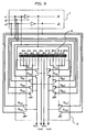
Fig.3 is a diagram of a switching circuit for
selecting slice thickness by changing output of a photo
diode array, which is a feature of the present
invention.
Fig.4 is a diagram illustrating the connection
of output of photo diode cells when various slice
thicknesses are selected in the present invention.
Fig.5 is a diagram of an X-ray detector in an
embodiment of the present invention, mounted on a
scanner rotating plate.
Fig.6 is a block diagram illustrating the whole
system of a multi-slice X-ray CT apparatus of the
present invention.
Fig.7 is a circuit diagram of a current/voltage
converting circuit for amplifying signals from the
photo diodes.
BEST MODE FOR CARRYING OUT THE INVENTION
Hereafter, an embodiment of a multi-slice
X-ray CT apparatus of the present invention will be
described with reference to the attached drawings.
Fig.5 is a diagram of an X-ray detector
mounted on a scanner rotating plate in an embodiment
of the present invention, and Fig.6 is a block diagram
of the whole system of the multi-slice X-ray CT
apparatus of the present invention.
In Fig.6, the whole system of a multi-slice
X-ray CT apparatus of the present invention comprises
three units, that is, a scanner 45, a console 46, and an
image processing unit 47. At the center of the
scanner 45, a scanner rotating plate 35 is supported so
as to freely rotate. On a scanner rotating plate 35, an
X-ray tube 36 is mounted opposite to an X-ray detector
38, an opening 41 provided between said X-ray tube 36
and said X-ray detector 38.
With reference to Fig.5, the arrangement of
the X-ray detector 38 on the scanner rotating plate 35
will be described. The X-ray detector 38 is arranged
opposite to the X-ray tube 36, and between said X-ray
detector 38 and said X-ray tube 36 is laid the object 42
inserted in the opening 41 of the scanner rotating plate
35. The X-ray detector 38 and the collimator plates
39 are contained in a detector container 37. The X-ray
detector 38 is comprised of a plurality of X-ray
detecting element arrays 10, which are polygonally
arranged around the focal point of the X-ray tube 36.
In front of the X-ray detecting element arrays 10, the
collimator plate 39 is radially arranged around the
focal point of the X-ray tube 36, said collimator plates
39 provided for preventing scattered X-rays that come
from the directions other than the focal point of the
X-ray tube is set from entering the X-ray detecting
element arrays 10. Also, the X-ray beam collimator 49
is disposed in front of the X-ray tube 36 to narrow an
X-ray beam in the slicing direction and in the channel
direction. In measurement performed by the X-ray
detector 38, the object 42 is inserted into the opening
41, and X-rays are radiated to the object 42 from the
focal point of the X-ray tube 36 while the scanner
rotating plate 35 is revolved, and the dose of the X-rays
transmitted from the each direction to the object 42 is
measured. Here, thickness in the slicing direction
and width in the channel directions of the X-ray beam
radiated from the focal point of the X-ray tube 36 are
narrowed by the X-ray beam collimator 49. The
output of the X-ray detector 38 is transmitted to an
amplifier 40. The output signals are amplified to an
adequate level in the amplifier 40, and then they are
subject to analog-digital conversion. Then, said
converted signals are sent to the image processing unit
47.
In Fig.6, console 46 contains a keyboard 54, a
scanning condition setting circuit 55 and an image
displaying unit 53, and controls the scanner 45 and
displaying a slice image of the object 42.
The scanning conditions of the scanner 45 are
input from the keyboard 54 on the console 46 to the
scanning condition setting means 55. In this
embodiment, a slice construction signal (that is, the
information indicating slice thickness × the number of
slices) 65 and an image adding signal 66 are sent to the
scanner 45 and the image processing unit 47
respectively, in accordance with information
concerning the slice thickness in the scanning
conditions.
The slice construction signal 65 is received by
a scanner control circuit 48 in the scanner 45. At this
time, a collimator opening control signal 67 and a
detector switch changing control signal 68 are
generated in accordance with said slice construction
signal 65, and said signals 67 and 68 are sent to the
X-ray beam collimator 49 and the X-ray detector 38
respectively. Then, according to the scanning
conditions, the slice thickness of the X-ray beam and
the conditions for switching the switching circuit for
the signals of the X-ray detecting elements in the
slicing direction are set. The outputs of the X-ray
detector 38 are amplified and then subject to
analog-digital conversion in the amplifier 40, and then
it is sent as measured data 69 for a plurality of slices
to the image processing unit 47.
The image processing unit 47 includes an
image reconstructing circuit 50, an image adder circuit
51, and a magnetic disc unit 52. In a multi-slice
X-ray CT apparatus, various tomograms can be
obtained by changing slice thickness of the X-ray
detector in measurement, and as well by adding
reconstructed images. For example, when tomograms
of 5mm slice thickness are measured for four pieces,
these four tomograms can be dealt with as two
tomograms of 10mm slice thickness by combining said
four tomograms into two pairs, and utilizing these
combined images in diagnosis. In this manner, the
image of thick slice width can be used when a lesion is
being searched for, and an image of thin slice width
can be used when the lesion is being minutely
examined. Thus, the efficiency of diagnosis can be
improved. Since the number of images obtained by a
multi-slice X-ray CT apparatus increases as compared
with those obtained with a conventional X-ray CT
apparatus, a dedicated image adder circuit 51 is
provided in said image processing unit 47. In the
image processing device 47, the image reconstructing
circuit 50 makes slice images of plural slice locations
using the measurement data 69 of corresponding rows
of X-ray detecting elements 38 in the slicing direction
sent from the scanner 45. Then, said plurality of slice
images is sent to image adder circuit 51. The image
adder circuit 51 performs adding of the reconstructed
slice images, in accordance with the image adder
signal 66 sent from the scanning condition setting
circuit 55 of the console 46. Final image data 70 thus
obtained is sent to the image displaying unit 53 on the
console 46, and stored in a memory unit such as
magnetic disc unit 52.
Next, the structure of an X-ray detecting
element array forming said X-ray detector will be
described.
Fig. 1 is an external view of an X-ray detecting
element array in an embodiment of the present
invention. In Fig.1, the scintillators 2 of the X-ray
detecting element array 10 are bonded on the light
reception plane of a photo diode array (not shown)
which is mounted on a photo diode array substrate,
also referred to as a print substrate. The combination
of the scintillator 2 and the photo diode 6 is divided
with an equal pitch in the channel direction and in the
slicing direction to form an array. This combination of
scintillator 2 and photo diode 6 comprises an X-ray
detecting element. In the figure, 12 elements (for 12
channels) are arranged in the channel direction
(longitudinal direction), and 16 elements (for 16 slices)
are arranged in the slicing direction (horizontal
direction). Thus, the total number of said elements is
192. The output of the photo diode 6 of each X-ray
detecting element is sent from the X-ray detecting
element array 10 to a connector 4 through a switch
array (which is also referred to as a switching circuit).
In this manner, said output is connected to an external
circuit. And, installation holes 5 are provided on the
print substrate 1 for fixing finished X-ray detecting
element array 10 on the detector container 37 in Fig.5,
by using screws or the like.
A required number of rows of X-ray detecting
elements is arrayed in the X-ray detecting element
array 10 in the channel direction, and data for desired
slice thickness is measured by changing the
combination of outputs of each detecting elements in
said switch array 3. Fig. 2 shows an example of
changing the slice thickness by switching the
combination of the outputs of said divided photo diode
cells 6. In the example of Fig.2, four slices of
arbitrarily chosen thickness are measured at one time.
Fig.2(a) illustrates the case of measuring at one time
four slices of "slice thickness 1" corresponding to the
basic division pitch of the detecting elements in the
slicing direction, separately reading the four slices in
the center. Fig.2(b) illustrates the case of measuring
at one time four slices of "slice thickness 2" by reading
outputs of combined pairs of slices. Similarly, Fig.2(c)
and (d) illustrate the case of measuring "slice
thickness 3" and "slice thickness 4" respectively.
Next, Fig.3 illustrates switch circuit 3, which
is the main part of the present invention, for selecting
a slice thickness by routing the outputs of the photo
diode array. Fig.3 shows the switch circuit for one
channel of the photo diode array. A similar switch
circuit is provided for each channel. When receiving a
slice thickness selection signal (that is, a detector
switch changing control signal 68 generated in the
scanner control circuit 48 in accordance with the slice
constructing signal 65 set by the scanning condition
setting circuit in Fig.2) is input from an external
circuit, each switching element (which is formed with a
field effect transistor is used in this embodiment)
operates such that all the channels simultaneously
connects the outputs of the combined cells in the same
direction to the external circuit. A driving signal for
connecting/disconnecting each switching element is
generated by a driving signal generating circuit 7
according to said slice thickness selection signal. And
the switching circuit 8 provided to receive the output
of each photo diode cell is controlled to read outputs of
cells in desired positions. In Fig.3, sixteen photo
diode cells (#1-#16) are arranged. In accordance with
the slice thickness selecting signal, the output of one
cell×four lines, two cells×four lines, and four cells×
four lines can be read. The photo diode cells and the
switching elements are arranged symmetrically. The
total number of the switching elements is decreased by
sending out the outputs of the cells that do not need to
be divided in the combination corresponding to the
selected slice thickness before inputting the output
signals of the cells to the switching elements. The
switching elements placed on a symmetric position
operate in the same way, and the outputs (Out1-Out4)
of the cells are also symmetrically transmitted to the
external circuit. The selection of slice thickness is
performed with signal lines s1-s3 described in the
upper part of Fig.3. s1 is a signal line for measuring
of one cell × four lines, s2 for measuring two cells × four
lines, and s4 for measuring four cells × four lines.
One of these signal lines is selected, or set to High
level, and others are not selected, or set to Low level.
When s1 is selected, that is, s2 and s3 are not
selected, the switching elements of QA2, QA2', QBG, GBG',
QCG, QCG' are connected, and the elements of other
cells are not. Thus, the outputs of the cells #7-#10
become Out1-Out4 and are connected to the external
circuit. At the same time, the outputs of other cells
#1-#6 and #11-#16 are connected to the ground.
Consequently, each cell and the signals taken out are
operated as described in Fig.4(a).
Next, when s2 is selected, that is, s1 and s3
are not selected, the switching elements of QA1, QA1',
QB2, QB2', QCG, QCG' are connected, and other element
are not. Thus, the outputs of the cells #5-#12 are
combined into pairs and become Out1-Out4 connected
to the external circuit. The outputs of other cells
#1-#4 and #13-#16 are connected to the ground.
Consequently, each cells and the signals to be taken
out are operated as described in Fig.4(b).
When s3 is selected, that is, s1 and s2 are not
selected, the switching elements of QA1, QA1', QB1, QB1',
QC2, QC2' are connected, and other elements are not.
Thus, the output of all the cells #1-#16 are combined
into four outputs and connected to the external circuit.
Consequently, the signals of each cell are connected as
described in Fig.4(c). As is clear in Fig.4, all of the
cells that are not connected to the measuring circuit
due to the above selection are connected to the ground.
By constructing the measuring circuit in this manner,
even when electric charge is generated when scattered
X-rays enter the cells that are not connected to the
measuring circuit, voltage is not generated in the
output line since said cells that are not connected to
the measuring circuit are connected to the ground.
Therefore, errors do not occur in the signals going to
the measuring circuit.
In this embodiment, the outputs of one cell ×
four lines, two cells×four lines, and four cells×four
lines are read. Also, when the outputs of three cells
× four lines or other combinations are read, the
outputs of the selected cells can be sent to the
measuring circuit by connecting the output of
unselected cells to the ground.
By using the thus constructed multi-slice
X-ray detector, the dose of the X-rays transmitted from
all direction along the circumference of plural slices of
object 42 which is put in scanner opening 41 can be
measured at one time. In the present invention, output
terminals of the switch arrays for selecting slice
thickness provided near the photo diode array that are
not connected to the external circuit are connected to
the ground. Thus, even when electric charge is
generated due to scattered X-rays entering the photo
diode cells that are not connected to the measuring
circuit, disturbance voltage is prevented from entering
the amplifier (current/voltage converting circuit)
connected to the switch arrays. Thus, errors in
measurement data can be avoided. Therefore, by
using this X-ray detector in an X-ray CT apparatus, the
X-ray CT apparatus for obtaining at one time a
plurality of slice tomograms with high diagnosability
can be provided.