EP1298810B1 - Portable type radio equipment - Google Patents
Portable type radio equipment Download PDFInfo
- Publication number
- EP1298810B1 EP1298810B1 EP02256779A EP02256779A EP1298810B1 EP 1298810 B1 EP1298810 B1 EP 1298810B1 EP 02256779 A EP02256779 A EP 02256779A EP 02256779 A EP02256779 A EP 02256779A EP 1298810 B1 EP1298810 B1 EP 1298810B1
- Authority
- EP
- European Patent Office
- Prior art keywords
- signal
- antenna
- circuit
- transmitting
- phase
- Prior art date
- Legal status (The legal status is an assumption and is not a legal conclusion. Google has not performed a legal analysis and makes no representation as to the accuracy of the status listed.)
- Expired - Lifetime
Links
- 238000001514 detection method Methods 0.000 claims description 33
- 238000004891 communication Methods 0.000 claims description 30
- 238000000034 method Methods 0.000 claims description 21
- 230000003247 decreasing effect Effects 0.000 claims description 4
- 230000004044 response Effects 0.000 claims description 3
- 230000003111 delayed effect Effects 0.000 claims description 2
- 230000011664 signaling Effects 0.000 claims 1
- 230000005540 biological transmission Effects 0.000 description 8
- 238000011156 evaluation Methods 0.000 description 8
- 238000010586 diagram Methods 0.000 description 7
- 238000005259 measurement Methods 0.000 description 7
- 230000006866 deterioration Effects 0.000 description 5
- 230000006870 function Effects 0.000 description 5
- 230000010363 phase shift Effects 0.000 description 5
- 239000003990 capacitor Substances 0.000 description 2
- 238000013461 design Methods 0.000 description 2
- 238000012545 processing Methods 0.000 description 2
- 230000001413 cellular effect Effects 0.000 description 1
- 238000007796 conventional method Methods 0.000 description 1
- 238000012937 correction Methods 0.000 description 1
- 230000000694 effects Effects 0.000 description 1
- 230000002708 enhancing effect Effects 0.000 description 1
- 238000002474 experimental method Methods 0.000 description 1
- 230000003071 parasitic effect Effects 0.000 description 1
- 230000005855 radiation Effects 0.000 description 1
- 239000013598 vector Substances 0.000 description 1
Images




Classifications
-
- H—ELECTRICITY
- H03—ELECTRONIC CIRCUITRY
- H03H—IMPEDANCE NETWORKS, e.g. RESONANT CIRCUITS; RESONATORS
- H03H7/00—Multiple-port networks comprising only passive electrical elements as network components
- H03H7/38—Impedance-matching networks
- H03H7/40—Automatic matching of load impedance to source impedance
-
- H—ELECTRICITY
- H01—ELECTRIC ELEMENTS
- H01Q—ANTENNAS, i.e. RADIO AERIALS
- H01Q1/00—Details of, or arrangements associated with, antennas
- H01Q1/12—Supports; Mounting means
- H01Q1/22—Supports; Mounting means by structural association with other equipment or articles
- H01Q1/24—Supports; Mounting means by structural association with other equipment or articles with receiving set
- H01Q1/241—Supports; Mounting means by structural association with other equipment or articles with receiving set used in mobile communications, e.g. GSM
- H01Q1/242—Supports; Mounting means by structural association with other equipment or articles with receiving set used in mobile communications, e.g. GSM specially adapted for hand-held use
-
- H—ELECTRICITY
- H04—ELECTRIC COMMUNICATION TECHNIQUE
- H04B—TRANSMISSION
- H04B1/00—Details of transmission systems, not covered by a single one of groups H04B3/00 - H04B13/00; Details of transmission systems not characterised by the medium used for transmission
- H04B1/02—Transmitters
- H04B1/04—Circuits
- H04B1/0458—Arrangements for matching and coupling between power amplifier and antenna or between amplifying stages
Definitions
- the present invention relates to a radio equipment of portable type, particularly to a radio equipment of portable type made in one unit with an antenna and capable of reducing the influence of the things around the antenna upon the characteristics of the antenna.
- a radio equipment or terminal of portable type has become thinner and more compact.
- a radio equipment of portable type should be at present very easy to carry with. Therefore, thin and compactness of the equipment is very important features.
- a human body affects an antenna mounted on radio equipment.
- a human body absorbs and scatters a radio wave of the frequency used in the radio equipment of portable type. Further, a human body fluctuates the antenna impedance used nearby.
- a human body acts as dielectric media with a permittivity of 50 or higher. Consequently, a human body deteriorates the radiation characteristics of an antenna.
- an antenna is positioned closer to the ear of the equipment user. This closer distance to the ear makes deterioration of the antenna characteristics more serious.
- FIG. 1 shows the deterioration of the antenna gain caused by the impedance fluctuation while the radio equipment is being operated, taking the equipment thickness as a parameter.
- the equipment thickness becomes thinner than 20 mm, the possibility of contacting the ear to the antenna increases, and when the antenna comes in contact with the ear, the antenna gain is largely deteriorated.
- the cause of this deterioration is the fluctuation in the antenna impedance due to the influence of a human body.
- A-human body has a very high dielectric constant.
- the electrical length of the antenna is regarded as to be equivalently long. In this case, the antenna resonance frequency deviates from a desired value, and the antenna impedance changes accordingly.
- the antenna impedance will shift from the optimum value when it is brought close to a human body.
- the antenna To radiate a radio wave from an antenna, the antenna must be powered first of all.
- the optimum condition to power the antenna is that the impedance of a feed line is the same value as the impedance of that antenna.
- the antenna impedance changes from the optimum value
- the power supplied through the feed line is reflected by the input end of the antenna and returned to a transmitting amplifier. Therefore, the power outputted from the amplifier to the antenna is reduced.
- This proposal includes the power amplifier disclosed by Jpn. Pat. Appln. KOKAI Publication No. 10-341117 .
- This conventional power amplifier detects the current consumption in the power amplifier and the power reflected by an antenna, and supplies these detected signals to the control circuit.
- This control circuit sends a control signal to a variable phase snifter based on the both detected signals, and corrects phase shifts occurred between the power amplifier and antenna.
- the above-mentioned conventional method can check the impedance only while communication is being made in some types of the system.
- CDMA system for example, only an incoming call can be accepted in standby mode, and the above-mentioned operation is impossible.
- Sending a radio wave unnecessarily except when making communication causes troubles in other systems, and is controlled by the Radio Law.
- EP 1 093 272 describes a transmitter and receiver designed to compensate for load fluctuations which induce mismatching of impedance between an antenna and a transmission signal path.
- US 5 564 086 describes a method and apparatus for enhancing characteristics of a linear transmitter which operates under varying antenna loads without having to use an isolator.
- EP 0 404 150 describes a circuit arrangement which compensates for mistuning of the antenna resonant circuit.
- EP 0 459 440 describes a transmitter apparatus which has a variable impedance circuit to allow the impedance to be changed in response to the battery voltage.
- US 4 965 607 describes an antenna coupler with an adjustable impedance for use in high frequency swept antenna systems.
- An object of the present invention is to provide a radio equipment of portable type capable of making good communication, which has a circuit configuration matched with an antenna without an influence of an ambience around the antenna.
- FIG. 2 is a block diagram showing a radio equipment of portable type according to one embodiment of the present invention.
- an antenna 101 is connected to a matching circuit 102 having the function of matching the impedance of an antenna.
- the matching circuit 102 is connected to a changeover switch 103.
- One end of the changeover switch 103 is connected to a reflection phase detector 104 for detecting the phase of the reflection signal reflected by the antenna, and the other end is connected to a transmitter-receiver 105 for generating a transmitting signal.
- the transmitter-receiver 105 is connected to a power supply 107 through an ammeter 106 for detecting the current value of the supply power.
- a control-circuit 108 is connected to the reflection phase detector 104 and ammeter 106, receiving a phase signal and a current signal detected by the detector 104 and ammeter 106.
- the control circuit 108 sends a control signal to the matching circuit 102 and changeover switch 103, controlling these circuits.
- the matching circuit 102 comprising an inductance and a variable capacitance element, can change the impedance value of the antenna 101 when the variable capacitance element is varied by the control signal from the control circuit 108.
- the reflection phase detector 104 containing a transmitting circuit (not shown), measures what extent the antenna 101 changes the phase of the signal transmitted from the inside transmitting circuit (not shown), by receiving the signal reflected by the antenna.
- the reflection signal from the terminal of the antenna 101 is changed by the circumstances around the antenna 101.
- This change in the reflection signal is as already explained with the prior art is generated based on the antenna impedance change, and can be considered equivalent to the impedance change. Therefore, if the correlation between the reflection phase Sp and the state of the antenna 101 is previously examined, it is possible to know the state of the antenna by the value of the reflection phase Sp from the antenna 101.
- the power supply circuit 107 powers the transmitter-receiver 105.
- the supplied power is modulated based on the digital data signal, e.g., audio and video signals, sent from a data signal generator (not shown), and it is converted also to a transmission frequency, thereby a transmitting signal is generated and transmitted from the antenna 101.
- the antenna 101 transmits a transmitting signal into the air, but a part of the signal returns to the transmitter-receiver 105 as a reflected wave. The reflection quantity of this reflected signal changes depending on the impedance value of the antenna 101.
- the impedance of the antenna 101 is changed by the circumstances surrounding the antenna, and the returned reflection signal is also changed.
- This reflection signal changes the gain and efficiency of the transmitting amplifier in the transmitter-receiver 105. Therefore, the fluctuation in this reflection signal causes a fluctuation in the current consumption of the transmitter-receiver 105.
- An ammeter 106 measures the fluctuation in the current consumption, and a current level SI is sent to the control circuit 108.
- the value of this current level SI is closely related to the situation in which the antenna is placed. Therefore, the current level SI can be used as an evaluation function for adjustment of the matching circuit.
- the signal received by the antenna 101 is supplied to the transmitter-receiver 105 through the matching circuit 102 and changeover switch 103. Processing of the received signal is equivalent to ordinary processing of a mobile terminal or at a base station, and detailed explanation will be omitted.
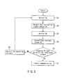
- control circuit 108 There will now be described the operations of the control circuit 108 with reference to the flow chart of FIG. 3.
- step S1 First, receiving the control signal from the control circuit 108, the movable contact of the switch 103 is connected to a first fixed contact Sa, setting a phase detection mode to detect the phase of the reflection signal (step S1).
- the transmitting circuit (not shown) of the phase detector 104 sends a phase detection signal to the control circuit 108, detecting the phase Sp of the reflection signal from the antenna 101 (step S2).
- the movable contact of the switch 103 is connected to a second fixed contact Sb, setting a current detection mode for detecting a transmission current (step S3). Therefore, the transmission power is supplied to the transmitter-receiver 105, the transmitting signal is supplied from the transmitter-receiver 105 to the antenna 101, and the ammeter 106 detects the current level SI of the power supplied to the transmitter-receiver 105 (step S4).
- the phase Sp and the current level SI of this reflection signal are given to the control circuit 108, where Sp and SI are compared to the reference values Sp0 and SI0 (step 55).
- the reference values Sp0 and SI0 are previously measured under the condition where the antenna 101 is not being close to the surrounding things, and the measurement value is stored in the storage circuit.
- Step S6 After this adjustment, the phase Sp and current value SI of the reflection signal will be measured in the same way, and the evaluation of these two values will be repeated. The adjustment and measurement will be repeated until the values of Sp and SI reach the reference values Sp0 and SI0, respectively.
- communication will be started in transmitting/receiving mode by utilizing the transmitter-receiver 105 (step S7).
- step S11 the movable contact of the switch 103 is connected to a fixed contact Sa by the control signal from the control circuit 108, and phase detection mode is set to detect the phase of the reflection signal (step S11).
- step S11 a transmitting signal is transmitted from the transmitting circuit (not shown) in the phase detector 104.
- the reflection signal from the antenna 101 is detected, and the phase Sp of the reflection signal is detected (step S12).
- a method of adjusting the matching circuit 102 is determined based on the value of the detected phase Sp (step S13).
- step 13 when comparing the current level Sp to the reference value Spa, the method of adjusting the capacitance element of the matching circuit depending on the phase shift value Sp, that is, whether to increase or decrease the capacitance is determined.
- the phase Sp of the reflection signal is largely shifted depending upon the design of the amplifier which comprises the transmitter-receiver, the value of the capacitance element of the matching circuit is increased or decreased to approximate the value Sp to the reference value. Whether to increase or decrease the capacitance, is determined.
- the movable contact of the switch 103 is connected to a second fixed contact Sb, and phase detection mode is set to detect the phase of the reflection signal (step S14).
- the current level SI is detected by the ammeter 106 (step S13).
- the current level SI is compared to the reference value SI0 (step S16).
- This reference value SI0 is, as explained above, is previously measured under the condition where the antenna 101 is not close to the surrounding things, and the measurement value is stored.
- the matching circuit 102 is adjusted (step S17). Measurement of the current value SI and evaluation will be repeated until the current level SI reaches the reference value SI0. When the current level SI reaches the reference value, communication will be started in transmitting/receiving mode by utilizing the transmitter-receiver 105 (step S18).
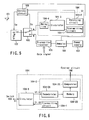
- FIG. 5 shows the configuration of the phase detector 104 of a radio equipment of portable type shown in FIG. 2.
- the blocks except the phase detector 104 are the same as those in FIG. 2, and the explanation thereof will be omitted.
- the phase detector 104 is provided with a transmitting circuit 104-1 which transmits a signal for measuring the phase of the reflection signal, and a receiving circuit 104-2 which receives the reflection signal as a reflected wave reflected by the antenna 101.
- the transmitting circuit 104-1 and the receiving circuit 104-2 are connected to a circulator 104-3.
- the circulator 104-3 is connected to a switch 103 through a delay line 104-4.
- the transmitting circuit 104-1 and the receiving circuit 104-2 include a phase modulator/demodulator.
- the circulator 104-3 sends the transmitting signal Si from the transmitting circuit 104-1 to the receiving circuit 104-2, sends the transmitting signal generated-from the transmitting circuit 104-1 to the antenna 101 through the delay line 104; and supplies the reflection signal reflected by the antenna 101 to the receiving circuit 104-2 through the delay line 104-4.
- the circulator 104-3 selectively supplies the receiving circuit 104-2 with the transmitting signal from the transmitting circuit 104-1 and the reflection signal from the antenna 101.
- the delay line 104-4 uses an element such as an acoustic surface-wave filter 10 to give a relatively long delay to the transmitting signal going to the antenna 101 and the reflection signal coming from the antenna.
- the receiving circuit 104-2 has the structure as shown in FIG. 6.
- the receiving circuit 104-2 includes a demodulator 104-2A which detects the transmitting signal or the reflection signal from the circulator 104-3, and demodulates them.
- the phase of the transmitting signal or the reflection signal demodulated by this de modulator 104-2A is stored as phase data in the storage circuit 104-2B.
- the stored phase data of the demodulated transmitting signal and reflection signal is sent to the comparator 104-2C, where the phase-difference between the two signals is detected.
- the detected phase-difference signal is supplied to the control circuit 108.
- the phase is detected in free space of the antenna 101 in order to determine a reference value of the phase.
- the following operations are executed under the condition where no things come close to the antenna.
- the movable contact of the switch 103 is connected to the fixed contact Sa by the control signal from the control circuit 108, and phase detection mode is set to detect the phase of the reflection signal (step S21).
- a transmitting signal is transmitted from the transmitting circuit 104-1. At this time, the signal is non-modulated, and the pulse width is fixed to be 1/2 or lower than the delay time of the delay line 104-4.
- the circulator 104-3 is previously adjusted, so that a part of the transmitted signal, that is, the transmitting signal S1 is sent directly to the receiving circuit 104-2 and the remainder, that is, the transmitting signal S2 is sent to the delay line 104-4.
- the receiving circuit 104-2 detects and demodulates the transmitting signal S1, and collects the phase data p1 of that signal, and starts measuring the time passing after the start of receiving the transmitting signal S1 (step S23)
- the transmitting signal S2 sent to the delay line 104-4 is transmitted to the antenna 101 through the delay line 104-4, the switch 103 and the matching circuit 102.
- the transmitting signal is reflected by the antenna 101 according to the impedance difference between the antenna 101 and the matching circuit 102.
- This reflected signal S2 is returned to the circulator 104-3 through the matching circuit 102, the switch 103 and the delay line 104-4.
- the reflected signal is applied to the receiving circuit 104-2 by the circulator 104-3.
- the receiving circuit 104-2 detects and demodulates the reflected signal S2, thereby obtaining the phase data P2 of the reflected signal S2 (step S24).
- the time measured after reception of the transmitting signal S1 is used. Namely, the back-and-fourth delay time given by the delay line 104-4 is previously measured. The input signal to be received after that delay time is judged to be the reflection signal S2 reflected by the antenna. As the signal 52 is delayed by the delay line 104-4, interference will not occur between the transmitting signal SI and the reflection signal S2.
- the comparator 104-2C compares the phase data P1 of the transmitting signal S1 with the phase data P2 of the reflection signal S2, and sends the phase-difference data P to the control circuit 108.
- the control circuit 108 stores in the memory this phase-difference data P indicating the state of the antenna in free space as a reference (step S25).
- the reference is determined.
- control circuit 108 compares the measured phase with the reference value.
- the method of adjusting the matching circuit 102 is determined based on the phase Sp of the detected reflection signal (step S27).
- this method determines a method of adjusting the capacitance element in the matching circuit according to the phase of the reflection signal when comparing the current value with the reference value, namely, whether to increase or decrease the capacitance.
- the phase shift of the reflection signal is largely depending upon the design of the amplifier which comprises the transmitter-receiver, the value of the capacitance element of the matching circuit is increased or decreased to approximate the current value to the reference value. Whether to increase or decrease the capacitance is determined.
- the movable contact of the switch 103 is connected to the fixed contact Sb, and current detection mode is set to detect the transmission current (step S28).
- the current level SI is detected by the ammeter 106 (step S29).
- the current level SI is compared to the reference value SIG (step S30).
- This reference value SI0 is, as explained above, is previously measured 25 under the conditions where the antenna 101 is not close to the surrounding things, and the measurement value is stored.
- the matching circuit 102 is adjusted (step S31). Measurement of the current value SI and evaluation will be repeated until the current level SI reaches the reference value SI0. When the current level SI reaches the reference value SI0, communication will be started in transmitting/receiving mode by utilizing the transmitter-receiver 105 (step S32).
- the communication performance of a mobile terminal when a human body or other surrounding things come close to the antenna can be improved.
- the frequencies used by the phase detector 108 and transmitter-receiver 105 need not to be strictly coincident.
- the effect of the present invention can be obtained with the similar frequencies.
- the reflection phase detector 108 preferably uses a frequency of IMS band (2.4 GHz). With this frequency, a signal to leak from the antenna 101 will not affect other mobile terminals.
- FIG. 9 shows the circuit of a radio equipment of portable type according to a further embodiment of the present invention.
- a common unit 110 is used for the switch 103 in the radio equipment of portable type shown in FIG. 2.
- the common unit 110 is composed of a filter, for example.
- the common unit 110 is given the same function as the switch 103. In other words, since the reflection wave generated by the phase detector 104 and reflected by the antenna has the frequency of SF1, it is prevented from being supplied to the phase detector 104 through the common unit 110.
- the reflection wave generated by the transmitter-receiver 105 and reflected by the antenna has the frequency of SF2, it is prevented from being supplied to the phase detector 104 through the common unit 110. If a radio equipment of portable type in which ISM band (2.4 GHz) is generated by the phase detector 104 is used, it is possible to check the antenna state of the portable radio equipment and to adjust the matching circuit 102 without affecting other radio equipments.
- ISM band 2.4 GHz
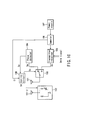
- FIG. 10 shows a circuit configuration of a radio equipment of portable type according to yet another embodiment of the invention.
- a second antenna 101-2 is provided in addition to the first antenna 101 and a matching circuit 102 is connected between the second antenna 101-2 and the ground, instead of the matching circuit 102 connected between the first antenna 101 and the switch 103.
- the second antenna 101-2 is so called a parasitic element, which can electro-magnetically coupled to the first antenna 101 under the control of an impedance of the matching circuit 102. If the first and second antennas 101, 101-2 are coupled each other, the antenna characteristics of the first antennas 101-2 are changed.
- a good radio communication can be achieved with a suitable antenna characteristics by matching an impedance of the matching circuit 102 under the control of the control section 108, as described in the same manner in the aforementioned embodiments, even if the antenna characteristic of the first antenna 101 shown in FIG. 10 is varied when the first antenna 101 is approached to the human boy.
- the matching circuit 102 may be located between a base or a tip portion of the second antenna 101-2 and the ground. In this configuration, there is a advantage that the gain is not prevented from being decreased due to the electrical power loss in the matching circuit 102, because the matching circuit 102 is not arrange between the first antenna 101 and the transmitter and receiver 105.
- the present invention is not limited to a mobile terminal and can be applicable to a variety of radio equipments having an antenna, including a radio base station, for example.
- the above embodiments employ a single matching circuit, which is a combination of the inductor and the variable capacitor such as a varactor diode whose capacitance is changed in accordance with an applied bias voltage.
- the circuit of the radio equipment may be provided with a plurality of matching circuits each having a fixed capacitor and inductor, and a high frequency switching circuit for switching one of the matching circuits under the control of the control circuit 108. According to this circuit, it is possible to obtain the same advantage as that of the embodiments in which the matching circuit is controlled.
- the ammeter 106 is utilized for estimating the electric power supplied to the transmitter-receiver 105, which is drive by a relatively low and substantially constant voltage. If a variable voltage drives the transmitter-receiver 105, instead of the relatively low and substantially constant voltage, it is required to use a power meter for measuring the power supplied to the transmitter-receiver 105, or use not only the ammeter for measuring a current supplied to the transmitter-receiver 105 but also a voltage meter for measuring the voltage applied to the transmitter-receiver 105 and calculate the power from the measured current and voltage.
Landscapes
- Engineering & Computer Science (AREA)
- Computer Networks & Wireless Communication (AREA)
- Signal Processing (AREA)
- Transmitters (AREA)
- Transceivers (AREA)
- Details Of Aerials (AREA)
Description
- The present invention relates to a radio equipment of portable type, particularly to a radio equipment of portable type made in one unit with an antenna and capable of reducing the influence of the things around the antenna upon the characteristics of the antenna.
- Recently, a radio equipment or terminal of portable type has become thinner and more compact. A radio equipment of portable type should be at present very easy to carry with. Therefore, thin and compactness of the equipment is very important features.
- On the other hand, there is a problem that a human body affects an antenna mounted on radio equipment. A human body absorbs and scatters a radio wave of the frequency used in the radio equipment of portable type. Further, a human body fluctuates the antenna impedance used nearby. Generally, in respect of a high frequency band, a human body acts as dielectric media with a permittivity of 50 or higher. Consequently, a human body deteriorates the radiation characteristics of an antenna.
- In addition, as the radio equipment of portable type becomes thin and compact, an antenna is positioned closer to the ear of the equipment user. This closer distance to the ear makes deterioration of the antenna characteristics more serious.
- The inventors of the present invention measured the influence of a human body on the deterioration of the antenna characteristics, and obtained the results as shown in FIG. 1. The experiment used a radio equipment of portable type of 2 GHz and measured the influence of a human body on the antenna. FIG. 1 shows the deterioration of the antenna gain caused by the impedance fluctuation while the radio equipment is being operated, taking the equipment thickness as a parameter. As seen from FIG. 1, when the equipment thickness becomes thinner than 20 mm, the possibility of contacting the ear to the antenna increases, and when the antenna comes in contact with the ear, the antenna gain is largely deteriorated.
- As mentioned above, the cause of this deterioration is the fluctuation in the antenna impedance due to the influence of a human body. A-human body has a very high dielectric constant. Thus, when the antenna is approached to a human body, the electrical length of the antenna is regarded as to be equivalently long. In this case, the antenna resonance frequency deviates from a desired value, and the antenna impedance changes accordingly.
- Therefore, even if the antenna impedance is adjusted to the optimum level in the radio equipment of portable type itself, the antenna impedance will shift from the optimum value when it is brought close to a human body.
- Further, when the antenna impedance is deteriorated, the transmission power of the radio equipment of portable type may be lowered. This problem will be explained hereinafter.
- To radiate a radio wave from an antenna, the antenna must be powered first of all. The optimum condition to power the antenna is that the impedance of a feed line is the same value as the impedance of that antenna.
- When the antenna impedance changes from the optimum value, the power supplied through the feed line is reflected by the input end of the antenna and returned to a transmitting amplifier. Therefore, the power outputted from the amplifier to the antenna is reduced.
- Moreover the reflected power deteriorates the amplifier performance, such as gain and operation efficiency, and causes deterioration of the transmission performance of the radio equipment itself.
- As a means of solving this problem, a method of examining the reflection coefficient between the amplifier and antenna has been proposed. This proposal includes the power amplifier disclosed by Jpn. Pat. Appln. KOKAI Publication
No. 10-341117 - Since this prior art power amplifier corrects only phase shifts, the evaluation quantity changing range is narrow and the phase shifts can be corrected by measuring the evaluation quantities. However, if a shift has two vectors, that is, the phase and amplitude directions of a reflection coefficient, as in the antenna of a cellular phone, the correction becomes difficult by only the above two evaluation quantities. Moreover, the antenna impedance must be checked even while communication is not made. Otherwise, communication has to be started in bad conditions, causing a communication failure. In the radio equipment of portable type, it is resulted from the high probability of changing the surrounding conditions upon start of communication. For example, when a call comes in standby mode, a mobile terminal is taken out from a pocket, held by hand, set to conversation mode, and attached to a head. The conditions around the antenna are changed three times in a very short time.
- The above-mentioned conventional method can check the impedance only while communication is being made in some types of the system. In the CDMA system, for example, only an incoming call can be accepted in standby mode, and the above-mentioned operation is impossible. Sending a radio wave unnecessarily except when making communication causes troubles in other systems, and is controlled by the Radio Law.
-
EP 1 093 272 -
US 5 564 086 describes a method and apparatus for enhancing characteristics of a linear transmitter which operates under varying antenna loads without having to use an isolator. -
EP 0 404 150 describes a circuit arrangement which compensates for mistuning of the antenna resonant circuit. -
EP 0 459 440 describes a transmitter apparatus which has a variable impedance circuit to allow the impedance to be changed in response to the battery voltage. -
US 4 965 607 describes an antenna coupler with an adjustable impedance for use in high frequency swept antenna systems. - As explained above, there is a problem in the conventional radio equipment of portable type. Antenna characteristics are deteriorated by bad matching between a transmitter and an antenna, caused by the surrounding conditions, particularly coming close to a human body.
- An object of the present invention is to provide a radio equipment of portable type capable of making good communication, which has a circuit configuration matched with an antenna without an influence of an ambience around the antenna.
- According to an aspect of the invention, there is provided a radio communication equipment as recited in
Claim 1. - According to a still further aspect of the invention, there is provided a method as recited in
Claim 10. - The invention can be more fully understood from the following detailed description when taken in conjunction with the accompanying drawings, in which:
- FIG. 1 is a graph showing the relation between the thickness of a mobile phone and the mismatching loss of an antenna;
- FIG. 2 is a block diagram showing schematically a circuit configuration of a radio equipment of portable type according to one embodiment of the present invention;
- FIG. 3 is a flow chart showing the operations of the radio equipment of portable type shown in FIG. 1;
- FIG. 4 is another flow chart showing the operations of the radio equipment of portable type shown in FIG. 1;
- FIG. 5 is a block diagram showing schematically a circuit configuration of a radio equipment of portable type according to another embodiment of the present invention;
- FIG. 6 is a block diagram showing the exemplary structure of the receiving circuit shown in FIG. 5;
- FIG. 7 is a flow chart showing the operations of the radio equipment of portable type shown in FIGS. 5 and 6;
- FIG. 8 is block diagram showing schematically a circuit configuration of a radio equipment of portable type which does not include both the first and second transmitting circuits of the claimed invention, by way of example;
- FIG. 9 is a block diagram showing schematically a circuit configuration of a radio equipment of portable type according to a further embodiment of the present invention; and
- FIG. 10 is a block diagram showing schematically the circuit of a radio equipment of portable type according to a yet further embodiment of the present invention.
- There will be described embodiments of the present invention with reference to the accompanying drawings. FIG. 2 is a block diagram showing a radio equipment of portable type according to one embodiment of the present invention.
- As shown in FIG. 2, an
antenna 101 is connected to amatching circuit 102 having the function of matching the impedance of an antenna. Thematching circuit 102 is connected to achangeover switch 103. One end of thechangeover switch 103 is connected to areflection phase detector 104 for detecting the phase of the reflection signal reflected by the antenna, and the other end is connected to a transmitter-receiver 105 for generating a transmitting signal. - The transmitter-
receiver 105 is connected to apower supply 107 through anammeter 106 for detecting the current value of the supply power. A control-circuit 108 is connected to thereflection phase detector 104 andammeter 106, receiving a phase signal and a current signal detected by thedetector 104 andammeter 106. Thecontrol circuit 108 sends a control signal to thematching circuit 102 andchangeover switch 103, controlling these circuits. - Here, the
matching circuit 102, comprising an inductance and a variable capacitance element, can change the impedance value of theantenna 101 when the variable capacitance element is varied by the control signal from thecontrol circuit 108. - The
reflection phase detector 104, containing a transmitting circuit (not shown), measures what extent theantenna 101 changes the phase of the signal transmitted from the inside transmitting circuit (not shown), by receiving the signal reflected by the antenna. As already described, the reflection signal from the terminal of theantenna 101 is changed by the circumstances around theantenna 101. This change in the reflection signal is as already explained with the prior art is generated based on the antenna impedance change, and can be considered equivalent to the impedance change. Therefore, if the correlation between the reflection phase Sp and the state of theantenna 101 is previously examined, it is possible to know the state of the antenna by the value of the reflection phase Sp from theantenna 101. It is also possible to determine the method of adjusting thematching circuit 102 by the measured reflection phase Sp, in order to return the reflection phase Sp to a reference level. Namely, by detecting the reflection signal from theantenna 101, the impedance of theantenna 101 can be estimated. If the value of the variable capacitance element of thematching circuit 102 is changed based on the impedance of theantenna 101, the transmission power can be held optimum. - The
power supply circuit 107 powers the transmitter-receiver 105. The supplied power is modulated based on the digital data signal, e.g., audio and video signals, sent from a data signal generator (not shown), and it is converted also to a transmission frequency, thereby a transmitting signal is generated and transmitted from theantenna 101. Theantenna 101 transmits a transmitting signal into the air, but a part of the signal returns to the transmitter-receiver 105 as a reflected wave. The reflection quantity of this reflected signal changes depending on the impedance value of theantenna 101. - The impedance of the
antenna 101 is changed by the circumstances surrounding the antenna, and the returned reflection signal is also changed. This reflection signal changes the gain and efficiency of the transmitting amplifier in the transmitter-receiver 105. Therefore, the fluctuation in this reflection signal causes a fluctuation in the current consumption of the transmitter-receiver 105. Anammeter 106 measures the fluctuation in the current consumption, and a current level SI is sent to thecontrol circuit 108. The value of this current level SI is closely related to the situation in which the antenna is placed. Therefore, the current level SI can be used as an evaluation function for adjustment of the matching circuit. - The signal received by the
antenna 101 is supplied to the transmitter-receiver 105 through thematching circuit 102 andchangeover switch 103. Processing of the received signal is equivalent to ordinary processing of a mobile terminal or at a base station, and detailed explanation will be omitted. - There will now be described the operations of the
control circuit 108 with reference to the flow chart of FIG. 3. - First, receiving the control signal from the
control circuit 108, the movable contact of theswitch 103 is connected to a first fixed contact Sa, setting a phase detection mode to detect the phase of the reflection signal (step S1). Next, the transmitting circuit (not shown) of thephase detector 104 sends a phase detection signal to thecontrol circuit 108, detecting the phase Sp of the reflection signal from the antenna 101 (step S2). - Next, the movable contact of the
switch 103 is connected to a second fixed contact Sb, setting a current detection mode for detecting a transmission current (step S3). Therefore, the transmission power is supplied to the transmitter-receiver 105, the transmitting signal is supplied from the transmitter-receiver 105 to theantenna 101, and theammeter 106 detects the current level SI of the power supplied to the transmitter-receiver 105 (step S4). The phase Sp and the current level SI of this reflection signal are given to thecontrol circuit 108, where Sp and SI are compared to the reference values Sp0 and SI0 (step 55). The reference values Sp0 and SI0 are previously measured under the condition where theantenna 101 is not being close to the surrounding things, and the measurement value is stored in the storage circuit. When the phase Sp and current level SI are deviated from the previously determined reference values Sp0 and SI0, respectively, thematching circuit 102 is adjusted. (Step S6) After this adjustment, the phase Sp and current value SI of the reflection signal will be measured in the same way, and the evaluation of these two values will be repeated. The adjustment and measurement will be repeated until the values of Sp and SI reach the reference values Sp0 and SI0, respectively. When the values of Sp and SI reach the reference values Sp0 and SI0, respectively, communication will be started in transmitting/receiving mode by utilizing the transmitter-receiver 105 (step S7). - Since communication is started after the antenna impedance is set to the optimum level, as described above, the influence of the circumstances upon the mobile terminal operation is eliminated and communication can be started in an optimum state.
- Next, another control method in the circuit shown of FIG. 2 will be explained with reference to the flow chart shown in FIG. 4. First, the movable contact of the
switch 103 is connected to a fixed contact Sa by the control signal from thecontrol circuit 108, and phase detection mode is set to detect the phase of the reflection signal (step S11). Next, a transmitting signal is transmitted from the transmitting circuit (not shown) in thephase detector 104. the reflection signal from theantenna 101 is detected, and the phase Sp of the reflection signal is detected (step S12). - Next, a method of adjusting the
matching circuit 102 is determined based on the value of the detected phase Sp (step S13). In step 13, when comparing the current level Sp to the reference value Spa, the method of adjusting the capacitance element of the matching circuit depending on the phase shift value Sp, that is, whether to increase or decrease the capacitance is determined. When the phase Sp of the reflection signal is largely shifted depending upon the design of the amplifier which comprises the transmitter-receiver, the value of the capacitance element of the matching circuit is increased or decreased to approximate the value Sp to the reference value. Whether to increase or decrease the capacitance, is determined. - After the adjustment method is determined, the movable contact of the
switch 103 is connected to a second fixed contact Sb, and phase detection mode is set to detect the phase of the reflection signal (step S14). Next, the current level SI is detected by the ammeter 106 (step S13). The current level SI is compared to the reference value SI0 (step S16). This reference value SI0 is, as explained above, is previously measured under the condition where theantenna 101 is not close to the surrounding things, and the measurement value is stored. - When the current level SI is shifted from the reference value SI0, the
matching circuit 102 is adjusted (step S17). Measurement of the current value SI and evaluation will be repeated until the current level SI reaches the reference value SI0. When the current level SI reaches the reference value, communication will be started in transmitting/receiving mode by utilizing the transmitter-receiver 105 (step S18). - Therefore, in such control, only the current value SI is used as an evaluation function for adjusting the
matching circuit 102. Accordingly, the time required by the adjustment can be reduced. As explained hereinbefore, the above-mentioned embodiment improves the communication performance of a mobile terminal when an antenna comes close to the surrounding things including a human body. FIG. 5 shows the configuration of thephase detector 104 of a radio equipment of portable type shown in FIG. 2. The blocks except thephase detector 104 are the same as those in FIG. 2, and the explanation thereof will be omitted. - As shown in FIG. 5, the
phase detector 104 is provided with a transmitting circuit 104-1 which transmits a signal for measuring the phase of the reflection signal, and a receiving circuit 104-2 which receives the reflection signal as a reflected wave reflected by theantenna 101. The transmitting circuit 104-1 and the receiving circuit 104-2 are connected to a circulator 104-3. The circulator 104-3 is connected to aswitch 103 through a delay line 104-4. - The transmitting circuit 104-1 and the receiving circuit 104-2 include a phase modulator/demodulator. The circulator 104-3 sends the transmitting signal Si from the transmitting circuit 104-1 to the receiving circuit 104-2, sends the transmitting signal generated-from the transmitting circuit 104-1 to the
antenna 101 through thedelay line 104; and supplies the reflection signal reflected by theantenna 101 to the receiving circuit 104-2 through the delay line 104-4. Namely, the circulator 104-3 selectively supplies the receiving circuit 104-2 with the transmitting signal from the transmitting circuit 104-1 and the reflection signal from theantenna 101. Further, the delay line 104-4 uses an element such as an acoustic surface-wave filter 10 to give a relatively long delay to the transmitting signal going to theantenna 101 and the reflection signal coming from the antenna. - The receiving circuit 104-2 has the structure as shown in FIG. 6. The receiving circuit 104-2 includes a demodulator 104-2A which detects the transmitting signal or the reflection signal from the circulator 104-3, and demodulates them. The phase of the transmitting signal or the reflection signal demodulated by this de modulator 104-2A is stored as phase data in the storage circuit 104-2B. The stored phase data of the demodulated transmitting signal and reflection signal is sent to the comparator 104-2C, where the phase-difference between the two signals is detected. The detected phase-difference signal is supplied to the
control circuit 108. - Description will now be given on the operations of the receiving
circuit 104 and thecontrol circuit 108 which have the phase detection function shown in FIG. 5 and FIG. 6, with reference with the flow chart of FIG. 7. In a first step, the phase is detected in free space of theantenna 101 in order to determine a reference value of the phase. The following operations are executed under the condition where no things come close to the antenna. - First, the movable contact of the
switch 103 is connected to the fixed contact Sa by the control signal from thecontrol circuit 108, and phase detection mode is set to detect the phase of the reflection signal (step S21). Next, a transmitting signal is transmitted from the transmitting circuit 104-1. At this time, the signal is non-modulated, and the pulse width is fixed to be 1/2 or lower than the delay time of the delay line 104-4. - The circulator 104-3 is previously adjusted, so that a part of the transmitted signal, that is, the transmitting signal S1 is sent directly to the receiving circuit 104-2 and the remainder, that is, the transmitting signal S2 is sent to the delay line 104-4. The receiving circuit 104-2 detects and demodulates the transmitting signal S1, and collects the phase data p1 of that signal, and starts measuring the time passing after the start of receiving the transmitting signal S1 (step S23)
- The transmitting signal S2 sent to the delay line 104-4 is transmitted to the
antenna 101 through the delay line 104-4, theswitch 103 and thematching circuit 102. The transmitting signal is reflected by theantenna 101 according to the impedance difference between theantenna 101 and thematching circuit 102. This reflected signal S2 is returned to the circulator 104-3 through thematching circuit 102, theswitch 103 and the delay line 104-4. The reflected signal is applied to the receiving circuit 104-2 by the circulator 104-3. The receiving circuit 104-2 detects and demodulates the reflected signal S2, thereby obtaining the phase data P2 of the reflected signal S2 (step S24). - To confirm the reflected signal S2, the time measured after reception of the transmitting signal S1 is used. Namely, the back-and-fourth delay time given by the delay line 104-4 is previously measured. The input signal to be received after that delay time is judged to be the reflection signal S2 reflected by the antenna. As the signal 52 is delayed by the delay line 104-4, interference will not occur between the transmitting signal SI and the reflection signal S2.
- The comparator 104-2C compares the phase data P1 of the transmitting signal S1 with the phase data P2 of the reflection signal S2, and sends the phase-difference data P to the
control circuit 108. Thecontrol circuit 108 stores in the memory this phase-difference data P indicating the state of the antenna in free space as a reference (step S25). - As described above, the reference is determined.
- Next, a measurement sequence will be described in an actual condition or environment. A method of measuring a phase in the actual condition is the same as the method of measuring the reference. Thus, procedures in the actual phase measuring method are the same as that of the steps S21 to S25. Thus, description of the procedures will be omitted.
- In the actual phase measuring method, after the step S26, the
control circuit 108 compares the measured phase with the reference value. - Next, the method of adjusting the
matching circuit 102 is determined based on the phase Sp of the detected reflection signal (step S27). As already explained, this method determines a method of adjusting the capacitance element in the matching circuit according to the phase of the reflection signal when comparing the current value with the reference value, namely, whether to increase or decrease the capacitance. When the phase shift of the reflection signal is largely depending upon the design of the amplifier which comprises the transmitter-receiver, the value of the capacitance element of the matching circuit is increased or decreased to approximate the current value to the reference value. Whether to increase or decrease the capacitance is determined. - After the adjustment method is determined, the movable contact of the
switch 103 is connected to the fixed contact Sb, and current detection mode is set to detect the transmission current (step S28). Next, the current level SI is detected by the ammeter 106 (step S29). The current level SI is compared to the reference value SIG (step S30). This reference value SI0 is, as explained above, is previously measured 25 under the conditions where theantenna 101 is not close to the surrounding things, and the measurement value is stored. - When the current level SI is shifted from the reference value SIO, the
matching circuit 102 is adjusted (step S31). Measurement of the current value SI and evaluation will be repeated until the current level SI reaches the reference value SI0. When the current level SI reaches the reference value SI0, communication will be started in transmitting/receiving mode by utilizing the transmitter-receiver 105 (step S32). - As explained above, the communication performance of a mobile terminal when a human body or other surrounding things come close to the antenna, can be improved.
- The frequencies used by the
phase detector 108 and transmitter-receiver 105 need not to be strictly coincident. The effect of the present invention can be obtained with the similar frequencies. - The
reflection phase detector 108 preferably uses a frequency of IMS band (2.4 GHz). With this frequency, a signal to leak from theantenna 101 will not affect other mobile terminals. - FIG. 9 shows the circuit of a radio equipment of portable type according to a further embodiment of the present invention. In this circuit, a
common unit 110 is used for theswitch 103 in the radio equipment of portable type shown in FIG. 2. Thecommon unit 110 is composed of a filter, for example. By making the frequency F1 of the transmitting signal SF1 generated by thephase detector 104 different from the frequency of the transmitting signal SF2 generated by the transmitter-receiver 105, thecommon unit 110 is given the same function as theswitch 103. In other words, since the reflection wave generated by thephase detector 104 and reflected by the antenna has the frequency of SF1, it is prevented from being supplied to thephase detector 104 through thecommon unit 110. Since the reflection wave generated by the transmitter-receiver 105 and reflected by the antenna has the frequency of SF2, it is prevented from being supplied to thephase detector 104 through thecommon unit 110. If a radio equipment of portable type in which ISM band (2.4 GHz) is generated by thephase detector 104 is used, it is possible to check the antenna state of the portable radio equipment and to adjust thematching circuit 102 without affecting other radio equipments. - Furthermore, FIG. 10 shows a circuit configuration of a radio equipment of portable type according to yet another embodiment of the invention. In FIG. 10, a second antenna 101-2 is provided in addition to the
first antenna 101 and amatching circuit 102 is connected between the second antenna 101-2 and the ground, instead of thematching circuit 102 connected between thefirst antenna 101 and theswitch 103. The second antenna 101-2 is so called a parasitic element, which can electro-magnetically coupled to thefirst antenna 101 under the control of an impedance of thematching circuit 102. If the first andsecond antennas 101, 101-2 are coupled each other, the antenna characteristics of the first antennas 101-2 are changed. Accordingly, a good radio communication can be achieved with a suitable antenna characteristics by matching an impedance of thematching circuit 102 under the control of thecontrol section 108, as described in the same manner in the aforementioned embodiments, even if the antenna characteristic of thefirst antenna 101 shown in FIG. 10 is varied when thefirst antenna 101 is approached to the human boy. Thematching circuit 102 may be located between a base or a tip portion of the second antenna 101-2 and the ground. In this configuration, there is a advantage that the gain is not prevented from being decreased due to the electrical power loss in thematching circuit 102, because thematching circuit 102 is not arrange between thefirst antenna 101 and the transmitter andreceiver 105. - It is apparent that although the above-mentioned embodiment uses a mobile terminal, the present invention is not limited to a mobile terminal and can be applicable to a variety of radio equipments having an antenna, including a radio base station, for example.
- Although, the above embodiments employ a single matching circuit, which is a combination of the inductor and the variable capacitor such as a varactor diode whose capacitance is changed in accordance with an applied bias voltage. However, the circuit of the radio equipment may be provided with a plurality of matching circuits each having a fixed capacitor and inductor, and a high frequency switching circuit for switching one of the matching circuits under the control of the
control circuit 108. According to this circuit, it is possible to obtain the same advantage as that of the embodiments in which the matching circuit is controlled. - In the embodiments described above, the
ammeter 106 is utilized for estimating the electric power supplied to the transmitter-receiver 105, which is drive by a relatively low and substantially constant voltage. If a variable voltage drives the transmitter-receiver 105, instead of the relatively low and substantially constant voltage, it is required to use a power meter for measuring the power supplied to the transmitter-receiver 105, or use not only the ammeter for measuring a current supplied to the transmitter-receiver 105 but also a voltage meter for measuring the voltage applied to the transmitter-receiver 105 and calculate the power from the measured current and voltage.
Claims (10)
- A radio communication equipment comprising:a power supply (107) configured to supply an electric power;a first transmitting circuit (105) configured to generate a first transmitting signal for communicating with the other communication equipment, which is energized by the power supply (107);a power detection circuit (106) configured to detect the electric power supplied to the first transmitting circuit (105) and generate a power detection signal;an antenna (101), having an antenna impedance, to which the first transmitting signal is supplied, and which generates an antenna reflection signal having a certain phase depending on the first transmitting signal;an impedance matching circuit (102), having a variable impedance, configured to adjust the variable impedance to match the antenna (101) with the first transmitting circuit (105); anda control circuit (108) configured to control the impedance matching circuit (102) to set the variable impedance depending on the power detection signal;characterized in that the radio communication equipment further comprises:a phase detection circuit (104) configured to generate a phase detection signal, the phase detection circuit (104) includinga second transmitting circuit (104-1) configured to generate a second transmitting signal having a first phase, and supply the second transmitting signal to the antenna (101), the antenna (101) generating an antenna (101) reflection signal having a second phase depending on the second transmitting signal, anda receiving circuit (104-2) configured to receive the second transmitting signal from the second transmitting circuit (104-1) and the antenna reflection signal from the antenna (101), and detect a phase-difference between the first and second phases to generate the phase detection signal; andthe control circuit (108) is configured to control the impedance matching circuit (102) to set the variable impedance depending on the phase detection signal in addition to the power detection signal.
- The radio communication equipment according to claim 1, characterized in that the radio communication equipment further comprises a selecting circuit (103) configured to select one of the phase detection circuit (104) and the first transmitting circuit (105) and connect the selected one of the phase detection circuit (104) and the first transmitting circuit (105) to the antenna (101), and the control circuit (108) is configured to control the selecting circuit (103) to receive the phase detection signal and the power detection signal.
- The radio communication equipment according to claim 2, characterized in that the control circuit (108) is configured to generate first and second selection signals and to supply the first and second selection signals to the selecting circuit (103), the selecting circuit (103) being configured to connect the antenna (101) to the phase detection circuit (104) in response to the first selecting signal, and to connect the antenna (101) to the transmitting circuit (105, 104-1) in response to the second signal.
- The radio communication equipment according to claim 1, characterized in that the control circuit (108) is configured to store a reference phase signal and a reference power signal, and to adjust the impedance of the impedance matching circuit (102) in accordance with the comparison between the phase detection signal and the reference phase signal, and between the power detection signal and the reference power signal.
- The radio communication equipment according to claim 3, characterized in that the control circuit (108) is configured to determine a method of adjusting the impedance matching circuit (102) depending on the comparison between the phase detection signal and the reference phase signal, and to compare the power detection signal with the reference power signal to set the variable impedance in the impedance matching circuit (102).
- The radio communication equipment according to claim 5, characterized in that the adjustment method corresponds to one of increasing and decreasing the variable impedance.
- The radio communication equipment according to claim 1, characterized by further comprising a second antenna (101-2) connected to the antenna (101), the first and second antennas (101, 101-2) being electro-magnetically coupled to each other.
- The radio communication equipment according to claim 1, characterized in that the phase detection circuit (104) further includes a delay line (104-4) configured to delay the second transmitting signal from the second transmitting circuit (104-1) to the antenna (101), and delay the antenna (101) reflection signal from the antenna (101) to the receiving circuit (104-2); and
a circulator (104-3) configured to circulate the delayed antenna (101) reflection signal to the receiving circuit (104-2), and circulate the second transmitting signal from the second transmitting circuit (104-1) to the delay line (104-4) and the receiving circuit (104-2). - The radio communication equipment according to claim 1, characterized in that the first transmitting signal has a first frequency, the second transmitting signal has a first phase and a second frequency, and the radio communication equipment further comprises a filter circuit configured to pass the first and second transmitting signal to the antenna (101) and the antenna (101) reflection signal to the phase detection circuit (104), respectively, and prevent the antenna (101) reflection signal from being transferred to the first transmitting circuit (105).
- A method of adjusting a variable impedance in an impedance matching circuit (102) connected to an antenna (101),
characterized by comprising:supplying an electric power to a first transmitting circuit (105) to generate a first transmitting signal and supplying the first transmitting signal to the antenna (101) through the impedance matching circuit (102) and communicating with the another communication equipment;detecting the electric power supplied to the first transmitting circuit (105) and generate a power detection signal;detecting an antenna reflection signal having a phase, which is returned from the antenna (101); andsetting the variable impedance of an impedance matching circuit (102) depending on the power detection signal, in order to match the antenna (101) with the first transmitting circuit (105):characterized in thatthe setting the variable impedance includesgenerating a second transmitting signal having a first phase by means of a second transmitting circuit (104-1), and supply the second transmitting signal to the antenna (101) which generates an antenna (101) reflection signal having a second phase depending on the second transmitting signal;receiving the second transmitting signal and the antenna reflection signal;detecting a phase-difference between the first and second phases to generate a phase detection signal, andcontrolling the variable impedance depending on the phase detection signal in addition to the power detection signal.
Applications Claiming Priority (2)
| Application Number | Priority Date | Filing Date | Title |
|---|---|---|---|
| JP2001295363 | 2001-09-27 | ||
| JP2001295363 | 2001-09-27 |
Publications (4)
| Publication Number | Publication Date |
|---|---|
| EP1298810A2 EP1298810A2 (en) | 2003-04-02 |
| EP1298810A3 EP1298810A3 (en) | 2004-12-15 |
| EP1298810B1 true EP1298810B1 (en) | 2007-08-08 |
| EP1298810B8 EP1298810B8 (en) | 2007-12-12 |
Family
ID=19116809
Family Applications (1)
| Application Number | Title | Priority Date | Filing Date |
|---|---|---|---|
| EP02256779A Expired - Lifetime EP1298810B8 (en) | 2001-09-27 | 2002-09-27 | Portable type radio equipment |
Country Status (4)
| Country | Link |
|---|---|
| US (2) | US6934557B2 (en) |
| EP (1) | EP1298810B8 (en) |
| CN (1) | CN1254925C (en) |
| DE (1) | DE60221613T2 (en) |
Cited By (7)
| Publication number | Priority date | Publication date | Assignee | Title |
|---|---|---|---|---|
| US8405563B2 (en) | 2006-01-14 | 2013-03-26 | Research In Motion Rf, Inc. | Adaptively tunable antennas incorporating an external probe to monitor radiated power |
| US8620247B2 (en) | 2006-01-14 | 2013-12-31 | Blackberry Limited | Adaptive impedance matching module (AIMM) control architectures |
| US8674783B2 (en) | 2008-09-24 | 2014-03-18 | Blackberry Limited | Methods for tuning an adaptive impedance matching network with a look-up table |
| US8781417B2 (en) | 2007-05-07 | 2014-07-15 | Blackberry Limited | Hybrid techniques for antenna retuning utilizing transmit and receive power information |
| US8787845B2 (en) | 2009-08-25 | 2014-07-22 | Blackberry Limited | Method and apparatus for calibrating a communication device |
| US9263806B2 (en) | 2010-11-08 | 2016-02-16 | Blackberry Limited | Method and apparatus for tuning antennas in a communication device |
| US9350405B2 (en) | 2012-07-19 | 2016-05-24 | Blackberry Limited | Method and apparatus for antenna tuning and power consumption management in a communication device |
Families Citing this family (67)
| Publication number | Priority date | Publication date | Assignee | Title |
|---|---|---|---|---|
| US8064188B2 (en) | 2000-07-20 | 2011-11-22 | Paratek Microwave, Inc. | Optimized thin film capacitors |
| US8744384B2 (en) | 2000-07-20 | 2014-06-03 | Blackberry Limited | Tunable microwave devices with auto-adjusting matching circuit |
| TWI220817B (en) * | 2003-08-22 | 2004-09-01 | Benq Corp | Antenna matching device and method thereof |
| WO2005055445A1 (en) * | 2003-12-05 | 2005-06-16 | Matsushita Electric Industrial Co., Ltd. | Mobile communication terminal |
| US7327802B2 (en) * | 2004-03-19 | 2008-02-05 | Sirit Technologies Inc. | Method and apparatus for canceling the transmitted signal in a homodyne duplex transceiver |
| JP4068587B2 (en) * | 2004-03-29 | 2008-03-26 | 埼玉日本電気株式会社 | Portable wireless communication terminal device |
| US7701728B2 (en) * | 2004-10-28 | 2010-04-20 | Kyocera Corporation | Electronic component module and radio comunications equipment |
| JP4606843B2 (en) * | 2004-11-01 | 2011-01-05 | 京セラ株式会社 | Wireless communication module, communication terminal, and impedance matching method |
| CN100533996C (en) * | 2005-01-31 | 2009-08-26 | 松下电器产业株式会社 | Mobile radio device capable of adaptive impedance matching |
| FI124618B (en) * | 2005-03-29 | 2014-11-14 | Perlos Oyj | Antenna system and method in conjunction with an antenna and antenna |
| US7586384B2 (en) * | 2005-08-15 | 2009-09-08 | Nokia Corporation | Integrated load impedance sensing for tunable matching networks |
| US7279979B2 (en) * | 2005-09-12 | 2007-10-09 | Nokia Corporation | Method and arrangement for adjusting an output impedance of a power amplifier |
| DE102005047155B4 (en) * | 2005-09-30 | 2011-05-19 | Infineon Technologies Ag | Transmission arrangement and method for impedance matching |
| US9406444B2 (en) | 2005-11-14 | 2016-08-02 | Blackberry Limited | Thin film capacitors |
| US7555276B2 (en) * | 2005-12-19 | 2009-06-30 | Sony Ericsson Mobile Communications Ab | Devices, methods, and computer program products for controlling power transfer to an antenna in a wireless mobile terminal |
| US8325097B2 (en) * | 2006-01-14 | 2012-12-04 | Research In Motion Rf, Inc. | Adaptively tunable antennas and method of operation therefore |
| KR101227678B1 (en) * | 2006-02-10 | 2013-01-30 | 삼성전자주식회사 | Human body communication system and method |
| US7714676B2 (en) | 2006-11-08 | 2010-05-11 | Paratek Microwave, Inc. | Adaptive impedance matching apparatus, system and method |
| US7535312B2 (en) | 2006-11-08 | 2009-05-19 | Paratek Microwave, Inc. | Adaptive impedance matching apparatus, system and method with improved dynamic range |
| US8299867B2 (en) * | 2006-11-08 | 2012-10-30 | Research In Motion Rf, Inc. | Adaptive impedance matching module |
| FR2909784B1 (en) * | 2006-12-06 | 2009-02-27 | Youcef Haddab | DEVICE FOR CONTROLLING THE OUTPUT POWER OF A RADIO FREQUENCY POWER AMPLIFIER. |
| CN101632232A (en) * | 2006-12-20 | 2010-01-20 | 熵敏通讯股份有限公司 | Impedance Control of Network Node Signal Interface |
| US7917104B2 (en) * | 2007-04-23 | 2011-03-29 | Paratek Microwave, Inc. | Techniques for improved adaptive impedance matching |
| US7825775B2 (en) * | 2007-07-31 | 2010-11-02 | Symbol Technologies, Inc. | Antenna-based trigger |
| US7991363B2 (en) * | 2007-11-14 | 2011-08-02 | Paratek Microwave, Inc. | Tuning matching circuits for transmitter and receiver bands as a function of transmitter metrics |
| US8614646B2 (en) * | 2008-03-14 | 2013-12-24 | Qualcomm Incorporated | Adaptive tunable antennas for wireless devices |
| US9143172B2 (en) * | 2009-06-03 | 2015-09-22 | Qualcomm Incorporated | Tunable matching circuits for power amplifiers |
| US8963611B2 (en) * | 2009-06-19 | 2015-02-24 | Qualcomm Incorporated | Power and impedance measurement circuits for a wireless communication device |
| US8072272B2 (en) | 2009-08-19 | 2011-12-06 | Qualcomm, Incorporated | Digital tunable inter-stage matching circuit |
| US9559639B2 (en) * | 2009-08-19 | 2017-01-31 | Qualcomm Incorporated | Protection circuit for power amplifier |
| US9026062B2 (en) * | 2009-10-10 | 2015-05-05 | Blackberry Limited | Method and apparatus for managing operations of a communication device |
| GB2476035B (en) * | 2009-12-08 | 2016-06-01 | Microsoft Technology Licensing Llc | Improvements relating to power amplifiers and antennas |
| CN101800561B (en) * | 2010-01-25 | 2014-04-09 | 中兴通讯股份有限公司 | Impedance matching device and method |
| US8798179B2 (en) * | 2010-02-02 | 2014-08-05 | Kyocera Corporation | Radio communication device |
| US8803631B2 (en) | 2010-03-22 | 2014-08-12 | Blackberry Limited | Method and apparatus for adapting a variable impedance network |
| CA2797074C (en) | 2010-04-20 | 2018-08-14 | Research In Motion Rf, Inc. | Method and apparatus for managing interference in a communication device |
| CN102347745A (en) * | 2010-08-04 | 2012-02-08 | 国基电子(上海)有限公司 | Adaptive impedance matching circuit |
| US20120071108A1 (en) * | 2010-09-20 | 2012-03-22 | Mediatek Inc. | Radio Frequency Signal Control Module and Radio Frequency Signal Controlling Method |
| CN102420353B (en) * | 2010-09-28 | 2015-08-05 | 宏达国际电子股份有限公司 | antenna module |
| CN102098243B (en) | 2010-12-29 | 2016-04-13 | 中兴通讯股份有限公司 | antenna impedance matching device and method |
| US8712340B2 (en) | 2011-02-18 | 2014-04-29 | Blackberry Limited | Method and apparatus for radio antenna frequency tuning |
| US8655286B2 (en) | 2011-02-25 | 2014-02-18 | Blackberry Limited | Method and apparatus for tuning a communication device |
| US8626083B2 (en) | 2011-05-16 | 2014-01-07 | Blackberry Limited | Method and apparatus for tuning a communication device |
| US8594584B2 (en) | 2011-05-16 | 2013-11-26 | Blackberry Limited | Method and apparatus for tuning a communication device |
| WO2013022826A1 (en) | 2011-08-05 | 2013-02-14 | Research In Motion Rf, Inc. | Method and apparatus for band tuning in a communication device |
| KR101305597B1 (en) * | 2011-08-08 | 2013-09-09 | 엘지이노텍 주식회사 | Impedance matching apparatus and method |
| JP5696058B2 (en) * | 2012-01-13 | 2015-04-08 | 株式会社東芝 | Power receiving device, power transmitting device and control device |
| KR101874892B1 (en) | 2012-01-13 | 2018-07-05 | 삼성전자 주식회사 | Small antenna appartus and method for controling a resonance frequency of small antenna |
| US9281849B2 (en) * | 2012-03-26 | 2016-03-08 | Google Technology Holdings LLC | Method and apparatus for compensating for phase shift in a communication device |
| US9048524B2 (en) | 2012-03-26 | 2015-06-02 | Google Technology Holdings LLC | Method and apparatus for compensating for phase shift in a communication device |
| US9014245B2 (en) | 2012-03-26 | 2015-04-21 | Google Technology Holdings LLC | Method and apparatus for compensating for phase shift in a communication device |
| US8948889B2 (en) | 2012-06-01 | 2015-02-03 | Blackberry Limited | Methods and apparatus for tuning circuit components of a communication device |
| US9853363B2 (en) | 2012-07-06 | 2017-12-26 | Blackberry Limited | Methods and apparatus to control mutual coupling between antennas |
| US9246223B2 (en) | 2012-07-17 | 2016-01-26 | Blackberry Limited | Antenna tuning for multiband operation |
| US9413066B2 (en) | 2012-07-19 | 2016-08-09 | Blackberry Limited | Method and apparatus for beam forming and antenna tuning in a communication device |
| US9362891B2 (en) | 2012-07-26 | 2016-06-07 | Blackberry Limited | Methods and apparatus for tuning a communication device |
| JP5762377B2 (en) | 2012-09-28 | 2015-08-12 | 太陽誘電株式会社 | Impedance matching circuit and antenna system |
| US9374113B2 (en) | 2012-12-21 | 2016-06-21 | Blackberry Limited | Method and apparatus for adjusting the timing of radio antenna tuning |
| US10404295B2 (en) | 2012-12-21 | 2019-09-03 | Blackberry Limited | Method and apparatus for adjusting the timing of radio antenna tuning |
| JP5700055B2 (en) * | 2013-01-17 | 2015-04-15 | 株式会社村田製作所 | Antenna device |
| CN104638362B (en) * | 2013-11-15 | 2019-05-21 | 深圳富泰宏精密工业有限公司 | Wireless communication device |
| CN103761950B (en) * | 2013-12-31 | 2016-02-24 | 深圳市华星光电技术有限公司 | For compensating the method for the data line impedance of liquid crystal display |
| US9438319B2 (en) | 2014-12-16 | 2016-09-06 | Blackberry Limited | Method and apparatus for antenna selection |
| KR102123283B1 (en) | 2016-08-18 | 2020-06-16 | 삼성전자 주식회사 | Electronic device and a method of identifying whether electronic device is gripped |
| CN111049600B (en) * | 2019-12-10 | 2022-03-04 | 航天信息股份有限公司 | Antenna debugging method and device, storage medium and electronic equipment |
| US12512583B2 (en) * | 2021-09-23 | 2025-12-30 | Semtech Corporation | Proximity sensor for RF control |
| CN114367055A (en) * | 2021-12-30 | 2022-04-19 | 深圳智能光谱有限公司 | head-mounted hair growth device |
Family Cites Families (22)
| Publication number | Priority date | Publication date | Assignee | Title |
|---|---|---|---|---|
| US3601717A (en) * | 1969-11-20 | 1971-08-24 | Gen Dynamics Corp | System for automatically matching a radio frequency power output circuit to a load |
| US4757745A (en) * | 1987-02-26 | 1988-07-19 | Vickers, Incorporated | Microwave antenna and dielectric property change frequency compensation system in electrohydraulic servo with piston position control |
| US4965607A (en) * | 1987-04-30 | 1990-10-23 | Br Communications, Inc. | Antenna coupler |
| US5170496A (en) * | 1989-06-22 | 1992-12-08 | Texas Instruments Deutschland Gmbh | Circuit arrangement for matching the resonant frequency of an antenna resonant circuit to the output frequency of a transmitter output stage |
| US5276912A (en) * | 1990-02-06 | 1994-01-04 | Motorola, Inc. | Radio frequency power amplifier having variable output power |
| JP2647730B2 (en) * | 1990-06-01 | 1997-08-27 | ソニー株式会社 | Mobile phone equipment |
| US5491715A (en) * | 1993-06-28 | 1996-02-13 | Texas Instruments Deutschland Gmbh | Automatic antenna tuning method and circuit |
| JP2974895B2 (en) * | 1993-09-16 | 1999-11-10 | 富士通株式会社 | Portable wireless devices |
| US5564086A (en) * | 1993-11-29 | 1996-10-08 | Motorola, Inc. | Method and apparatus for enhancing an operating characteristic of a radio transmitter |
| US5869968A (en) * | 1994-03-11 | 1999-02-09 | Baker Hughes Incorporated | Method and apparatus for avoiding mutual coupling between receivers in measurement while drilling |
| JP2728018B2 (en) * | 1995-04-18 | 1998-03-18 | 日本電気株式会社 | Transmission circuit |
| GB2317760B (en) * | 1996-09-27 | 2000-09-13 | Nec Technologies | Mobile telephone apparatus |
| JP3475037B2 (en) * | 1997-03-14 | 2003-12-08 | 株式会社東芝 | transceiver |
| JP3019802B2 (en) | 1997-06-09 | 2000-03-13 | 日本電気株式会社 | Power amplifier |
| EP0940690A3 (en) * | 1998-03-05 | 2000-11-29 | The Whitaker Corporation | Microwave sensor for object motion detection |
| JP2000216610A (en) * | 1998-11-19 | 2000-08-04 | Nec Corp | Method and device for sensing and informing contact of human body with antenna for portable telephone set |
| JP2000295055A (en) | 1999-04-01 | 2000-10-20 | Matsushita Electric Ind Co Ltd | Transmitter and receiver |
| JP3776632B2 (en) | 1999-06-28 | 2006-05-17 | Necネットワーク・センサ株式会社 | Power amplifier |
| JP2002064386A (en) * | 2000-08-23 | 2002-02-28 | Sony Corp | Matching device |
| US6570462B2 (en) * | 2000-11-08 | 2003-05-27 | Research In Motion Limited | Adaptive tuning device and method utilizing a surface acoustic wave device for tuning a wireless communication device |
| US6961368B2 (en) * | 2001-01-26 | 2005-11-01 | Ericsson Inc. | Adaptive antenna optimization network |
| US6710651B2 (en) * | 2001-10-22 | 2004-03-23 | Kyocera Wireless Corp. | Systems and methods for controlling output power in a communication device |
-
2002
- 2002-09-27 EP EP02256779A patent/EP1298810B8/en not_active Expired - Lifetime
- 2002-09-27 US US10/256,080 patent/US6934557B2/en not_active Expired - Lifetime
- 2002-09-27 DE DE60221613T patent/DE60221613T2/en not_active Expired - Fee Related
- 2002-09-27 CN CN02143512.XA patent/CN1254925C/en not_active Expired - Fee Related
-
2005
- 2005-07-18 US US11/183,009 patent/US20050261036A1/en not_active Abandoned
Non-Patent Citations (1)
| Title |
|---|
| None * |
Cited By (8)
| Publication number | Priority date | Publication date | Assignee | Title |
|---|---|---|---|---|
| US8405563B2 (en) | 2006-01-14 | 2013-03-26 | Research In Motion Rf, Inc. | Adaptively tunable antennas incorporating an external probe to monitor radiated power |
| US8620247B2 (en) | 2006-01-14 | 2013-12-31 | Blackberry Limited | Adaptive impedance matching module (AIMM) control architectures |
| US8620246B2 (en) | 2006-01-14 | 2013-12-31 | Blackberry Limited | Adaptive impedance matching module (AIMM) control architectures |
| US8781417B2 (en) | 2007-05-07 | 2014-07-15 | Blackberry Limited | Hybrid techniques for antenna retuning utilizing transmit and receive power information |
| US8674783B2 (en) | 2008-09-24 | 2014-03-18 | Blackberry Limited | Methods for tuning an adaptive impedance matching network with a look-up table |
| US8787845B2 (en) | 2009-08-25 | 2014-07-22 | Blackberry Limited | Method and apparatus for calibrating a communication device |
| US9263806B2 (en) | 2010-11-08 | 2016-02-16 | Blackberry Limited | Method and apparatus for tuning antennas in a communication device |
| US9350405B2 (en) | 2012-07-19 | 2016-05-24 | Blackberry Limited | Method and apparatus for antenna tuning and power consumption management in a communication device |
Also Published As
| Publication number | Publication date |
|---|---|
| US6934557B2 (en) | 2005-08-23 |
| CN1254925C (en) | 2006-05-03 |
| US20030060227A1 (en) | 2003-03-27 |
| CN1411099A (en) | 2003-04-16 |
| US20050261036A1 (en) | 2005-11-24 |
| EP1298810A2 (en) | 2003-04-02 |
| EP1298810A3 (en) | 2004-12-15 |
| EP1298810B8 (en) | 2007-12-12 |
| DE60221613T2 (en) | 2007-12-06 |
| DE60221613D1 (en) | 2007-09-20 |
Similar Documents
| Publication | Publication Date | Title |
|---|---|---|
| US6934557B2 (en) | Portable type radio equipment | |
| CA2519371C (en) | System and method for regulating antenna electrical length | |
| KR100748732B1 (en) | Wireless communications module, communication terminal and impedance matching method | |
| US6895225B1 (en) | System for matching an antenna for a wireless communication device | |
| EP1633018A2 (en) | Antenna apparatus of mobile communications terminal and operation method thereof | |
| US8131331B2 (en) | Portable and foldable radio terminal with multiple frequency antenna | |
| US6944433B2 (en) | Portable telephone apparatus that can attain directivity of antenna which optimizes reception state from base station | |
| US8472904B2 (en) | Antenna with integrated tuning detection elements | |
| US6771944B2 (en) | Diversity receiver continuously responsive to best signal | |
| EP1505727B1 (en) | A portable radio apparatus | |
| JP2003174367A (en) | Portable radio | |
| JP3927918B2 (en) | Wireless communication device and wireless communication method | |
| JP3717741B2 (en) | Automatic tuning antenna system | |
| WO2000035124A2 (en) | Dual antenna system | |
| JPH11136157A (en) | Mobile radio terminal equipment | |
| JP3726055B2 (en) | Antenna circuit device for mobile phone | |
| JP2007166534A (en) | Receiver circuit | |
| KR20050067297A (en) | Method and apparatus of minimize body effect for mobile phone antenna | |
| US20060063557A1 (en) | Portable radio | |
| JPH11150496A (en) | Antenna device and portable wireless device | |
| JP3973958B2 (en) | Receiver with antenna self-check function | |
| KR100693642B1 (en) | ERP compensation device in mobile communication terminal | |
| JP2004260514A (en) | Wireless portable terminal device | |
| KR101241773B1 (en) | Antenna matching device, wireless communication device, and method and recording medium thereof | |
| JPH05291854A (en) | Automatic power control circuit |
Legal Events
| Date | Code | Title | Description |
|---|---|---|---|
| PUAI | Public reference made under article 153(3) epc to a published international application that has entered the european phase |
Free format text: ORIGINAL CODE: 0009012 |
|
| 17P | Request for examination filed |
Effective date: 20021014 |
|
| AK | Designated contracting states |
Kind code of ref document: A2 Designated state(s): AT BE BG CH CY CZ DE DK EE ES FI FR GB GR IE IT LI LU MC NL PT SE SK TR |
|
| AX | Request for extension of the european patent |
Extension state: AL LT LV MK RO SI |
|
| PUAL | Search report despatched |
Free format text: ORIGINAL CODE: 0009013 |
|
| AK | Designated contracting states |
Kind code of ref document: A3 Designated state(s): AT BE BG CH CY CZ DE DK EE ES FI FR GB GR IE IT LI LU MC NL PT SE SK TR |
|
| AX | Request for extension of the european patent |
Extension state: AL LT LV MK RO SI |
|
| AKX | Designation fees paid |
Designated state(s): DE FR GB |
|
| 17Q | First examination report despatched |
Effective date: 20050923 |
|
| GRAP | Despatch of communication of intention to grant a patent |
Free format text: ORIGINAL CODE: EPIDOSNIGR1 |
|
| GRAS | Grant fee paid |
Free format text: ORIGINAL CODE: EPIDOSNIGR3 |
|
| GRAA | (expected) grant |
Free format text: ORIGINAL CODE: 0009210 |
|
| AK | Designated contracting states |
Kind code of ref document: B1 Designated state(s): DE FR GB |
|
| REG | Reference to a national code |
Ref country code: GB Ref legal event code: FG4D |
|
| REF | Corresponds to: |
Ref document number: 60221613 Country of ref document: DE Date of ref document: 20070920 Kind code of ref document: P |
|
| RIN2 | Information on inventor provided after grant (corrected) |
Inventor name: TSUJIMURA,AKIHIRO.INTELLECTUAL PROPERTY DIVISION Inventor name: KAYANO,HIROYUKI.C/O.INTELLECTUAL PROPERTY DIVISION Inventor name: MURAKAMI,YASUSHI.INTELLECTUAL PROPERTY DIVISION Inventor name: INOUE,KAZUHIRO.INTELLECTUAL PROPERTY DIVISION Inventor name: ITOH,TAKAYOSHI.C/O INTELLECTUAL PROPERTY DIVISION Inventor name: ODACHI,NORIAKI.INTELLECTUAL PROPERTY DIVISION Inventor name: SEKINA, SYU-ICHI,C/O KABUSHIKI KAISHA TOSHIBA Inventor name: YAMAGUCHI KEIICHI.INTELLECTUAL PROPERTY DIVISION Inventor name: ISEKI,YUJI.C/O INTELLECTUAL PROPERTY DIVISION Inventor name: ONO,NAOKO.C/O INTELLECTUAL PROPERTY DIVISION |
|
| ET | Fr: translation filed | ||
| PLBE | No opposition filed within time limit |
Free format text: ORIGINAL CODE: 0009261 |
|
| STAA | Information on the status of an ep patent application or granted ep patent |
Free format text: STATUS: NO OPPOSITION FILED WITHIN TIME LIMIT |
|
| 26N | No opposition filed |
Effective date: 20080509 |
|
| PGFP | Annual fee paid to national office [announced via postgrant information from national office to epo] |
Ref country code: FR Payment date: 20080915 Year of fee payment: 7 |
|
| PGFP | Annual fee paid to national office [announced via postgrant information from national office to epo] |
Ref country code: DE Payment date: 20081002 Year of fee payment: 7 |
|
| PGFP | Annual fee paid to national office [announced via postgrant information from national office to epo] |
Ref country code: GB Payment date: 20081001 Year of fee payment: 7 |
|
| GBPC | Gb: european patent ceased through non-payment of renewal fee |
Effective date: 20090927 |
|
| REG | Reference to a national code |
Ref country code: FR Ref legal event code: ST Effective date: 20100531 |
|
| PG25 | Lapsed in a contracting state [announced via postgrant information from national office to epo] |
Ref country code: DE Free format text: LAPSE BECAUSE OF NON-PAYMENT OF DUE FEES Effective date: 20100401 Ref country code: FR Free format text: LAPSE BECAUSE OF NON-PAYMENT OF DUE FEES Effective date: 20090930 |
|
| PG25 | Lapsed in a contracting state [announced via postgrant information from national office to epo] |
Ref country code: GB Free format text: LAPSE BECAUSE OF NON-PAYMENT OF DUE FEES Effective date: 20090927 |