EP1296458A1 - Five-port receiver with passive isolation - Google Patents
Five-port receiver with passive isolation Download PDFInfo
- Publication number
- EP1296458A1 EP1296458A1 EP01122741A EP01122741A EP1296458A1 EP 1296458 A1 EP1296458 A1 EP 1296458A1 EP 01122741 A EP01122741 A EP 01122741A EP 01122741 A EP01122741 A EP 01122741A EP 1296458 A1 EP1296458 A1 EP 1296458A1
- Authority
- EP
- European Patent Office
- Prior art keywords
- port
- passive
- junction device
- signals
- input
- Prior art date
- Legal status (The legal status is an assumption and is not a legal conclusion. Google has not performed a legal analysis and makes no representation as to the accuracy of the status listed.)
- Granted
Links
Images


Classifications
-
- H—ELECTRICITY
- H03—ELECTRONIC CIRCUITRY
- H03D—DEMODULATION OR TRANSFERENCE OF MODULATION FROM ONE CARRIER TO ANOTHER
- H03D3/00—Demodulation of angle-, frequency- or phase- modulated oscillations
- H03D3/007—Demodulation of angle-, frequency- or phase- modulated oscillations by converting the oscillations into two quadrature related signals
-
- H—ELECTRICITY
- H04—ELECTRIC COMMUNICATION TECHNIQUE
- H04B—TRANSMISSION
- H04B1/00—Details of transmission systems, not covered by a single one of groups H04B3/00 - H04B13/00; Details of transmission systems not characterised by the medium used for transmission
- H04B1/06—Receivers
- H04B1/16—Circuits
- H04B1/30—Circuits for homodyne or synchrodyne receivers
Definitions
- the present invention generally relates to the field of five-port receivers, especially to a five-port junction device for the processing of modulated RF signals, a mobile receiver comprising a five-port junction device and to a method for processing said RF signals.
- N-port network technology can successfully be used for a direct downconversion of RF modulated signals.
- One of the network topologies being well-known to the art is five-port topology using three power sensors.
- Six-port receivers as disclosed in the European patent application EP-A-0 896 455 are known for enabling a direct downconversion of received modulated RF signals from millimeter wave and microwave range to the baseband. Thereby, the six-port receiver detects the phase difference and the amplitude ratio of two incoming RF signals by using the information of superimposed, mutually interfering RF signals.
- a classical I/Q demodulator is not needed. With the aid of suitable calibration procedures the influence of non-ideal linear RF components (including manufacturing tolerances of these components) can be minimized.
- the circuitry of six-port receivers can be realized by only employing passive components in combination with power sensors for the detection of the phase difference and the amplitude ratio of said RF signals.
- An important feature of six-port receivers is that fabrication tolerances of the employed RF components can be calibrated, which inherently allows the usage of low-cost RF components.
- a structure for a six-port receiver is proposed in the IEEE MTT Symposium report "A Six-Port Direct Digital Millimeter Wave Receiver” (vol. 3, pp. 1659 to 1662, San Diego, May 1994) of Ji Li, R. G. Bossisio and Ke Wu. Therein, a novel scheme for a digital phase demodulation of modulated millimeter and microwave waves by means of a six-port receiver is presented. Due to said scheme some disadvantages of conventional receivers, wherein I/Q demodulators are used for a direct downconversion of the received RF signals, are overcome.
- Six-port technique is known to accurately measure both amplitude and phase of the scattering parameters in a microwave network. Instead of using heterodyne receivers, a six-port receiver accomplishes direct measurements at millimeter and microwave frequencies to perform a direct demodulation of received RF signals by extracting power levels at four of the six ports.
- the imperfections of the hardware such as phase errors of the bridges, imbalance of the power detectors, etc. can readily be eliminated by means of an appropriate calibration procedure.
- Six-port junction receivers consist of passive microwave components such as directional couplers and power dividers as well as diode detectors.
- the underlying circuit can easily be integrated as a Monolithic Microwave Integrated Circuit (MMIC).
- MMIC Monolithic Microwave Integrated Circuit
- a five-port junction device which can be used for processing received RF signals in order to perform a direct downconversion of said RF signals.
- the device comprises a passive four-port network being connected with a passive three-port network by means of a phase shifter. Thereby, one port of said passive four-port network acts as an input port used for the input of a first RF signal, and two ports of said passive four-port network act as output ports.
- the passive three-port comprises one port used for the input of a second RF signal and one output port.
- a passive isolation is provided as depicted in Figs. 2a+b.
- phase shifters are applied along with four passive structures, which provide a signal splitting and combine functional features.
- the output ports respectively provide output signals which can be obtained as linear combinations of the first and the second RF signal.
- the DSP is provided to calculate the complex ratio of the first and the second RF signal on the basis of the three power levels P 1 , P 2 and P 3 detected by the power sensors.
- the PCT patent application PCT/EP98/08329 refers to a N-port junction device (with N ⁇ 4) used in the receiver of a mobile telecommunications device for processing modulated RF signals comprising two RF input ports, two passive signal combining units connected to each other by means of a phase shifting element, wherein the first one of said passive signal combining units is fed with a first RF input signal and the second one of said passive signal combining units is fed with a second RF input signal.
- said N-port junction device comprises at least two power sensors, each connected to one of the output ports of said passive signal combining units.
- N-port RF receiver (with N ⁇ 3) for modulated RF signals is proposed, which is based on a N-port junction providing an isolation between the RF signal and the LO signal.
- the disclosed N-port junction is supplied with a first RF signal at a first input port (RF port) and with a second RF signal originating from a local oscillator (LO) at a second input port (LO port).
- the N-port junction contains a RF/LO isolation block comprising a non-reciprocal active circuitry for isolating the LO signal from the RF signal.
- a RF/LO isolation block comprising a non-reciprocal active circuitry for isolating the LO signal from the RF signal.
- hybrid microwave printed circuits An alternative way to provide isolation by passive means is the usage of hybrid microwave printed circuits.
- this approach requires a specific implementation topology and a four-port approach, wherein usually one port is out of use and has to be terminated by an impedance of 50 ⁇ .
- several of those hybrid microwave printed circuits are combined in order to provide the required phase shifts.
- each of the applied network solutions used for a demodulation of received RF signals is optimized to a specific purpose, and thus contains certain limitations.
- the network topology disclosed in the preferred embodiment of the European patent application EP 0 957 573 A1 only works in case of a four-port receiver structure, and also in the case when the intensity of the received signal does not play an important role, for example in case of PSK modulation.
- the underlying invention describes a low-complexity and low-effort solution for a five-port network topology of a mobile radio receiver used for demodulation of received modulated RF signals which can easily be realized.
- the invention is specially optimized for an isolation between said received modulated RF signal and a further RF signal originating from a local oscillator (LO) used for the downconversion of said received modulated RF signal.
- LO local oscillator
- a simple passive network topology which does not need any active devices for the purpose of isolation between the LO and RF input signals. Instead, it exhibits a topology comprising three phase shifters, four passive structures and several additional features which shall be described in the following sections. Said topology can easily be integrated in a Monolithic Microwave Integrated Circuit (MMIC).
- MMIC Monolithic Microwave Integrated Circuit
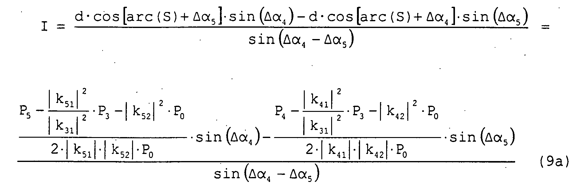
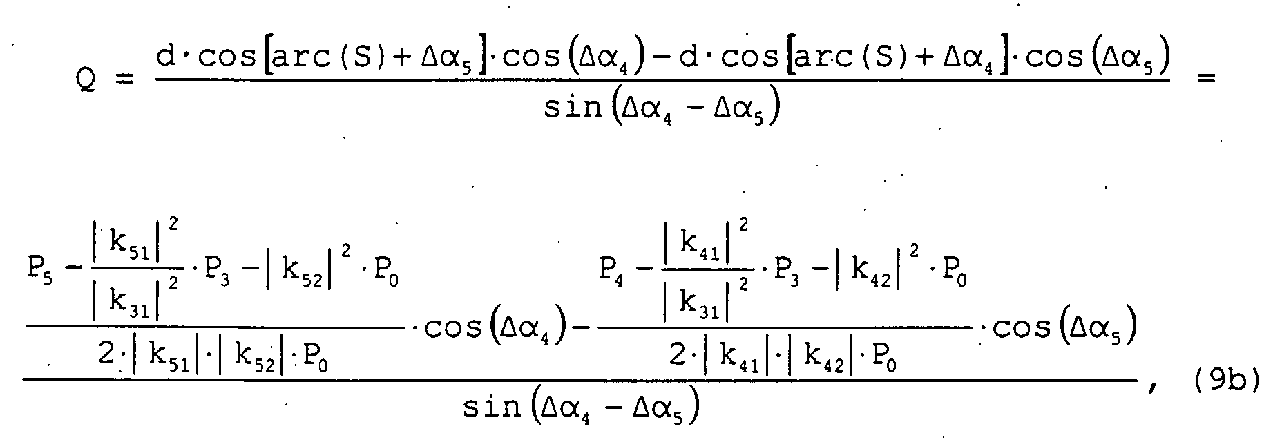
- the I/Q values can be calculated by combination of only two unknowns, for example the power values P 3 and P 5 for the I values and P 3 and P 4 for the Q values, respectively.
- the solution according to the underlying invention as depicted in Fig. 4 enables a significant reduction of the digital processing efforts.
- An optional resistive solution of the embodiment depicted in Fig. 4 is presented in Fig. 5.
- the independent claim 1 and the dependent claims 2 to 12 refer to a five-port junction device used for the processing of modulated RF signals in a mobile radio receiver.
- said five-port junction device comprises
- the non-reciprocal circuitry according to the preferred embodiment of the underlying invention comprises two branches, in which the first branch contains at least one phase shifter and the second branch contains at least two phase shifters, wherein the first end of each particular branch is connected to the first passive N-port network, and the second end of each branch is connected to the second passive N-port network in order to provide a passive isolation of the two RF input signals (S 1 and S 2 ).
- independent claim 13 and the dependent claim 14 relate to a mobile radio receiver comprising a five-port junction device according to anyone of the claims 1 to 12 for a direct downconversion of a received modulated RF input signal (S 1 ).
- the independent claim 15 and the dependent claim 16 pertain to a method for supporting a direct downconversion of received modulated RF signals.
- a mobile radio receiver comprising a five-port junction device used for the processing of modulated RF signals according to anyone of the claims 1 to 14 is applied.
- the dependent claims 17 and 18 refer to a method for providing a calibration of the five-port junction device according to anyone of the claims 1 to 12. Thereby, an isolation of the RF input signals (S 1 and S 2 ) is achieved by means of a phase shift of at least one of said RF input signals (S 1 and S 2 ). Due to said method it can be ensured that after having performed said phase shifts the obtained values for the phases of said RF input signals (S 1 and S 2 ) are different.
- the dependent patent claims 19 to 21 refer to a mobile telecommunications device, wherein a mobile radio receiver according to anyone of the claims 13 and 14, a method for a direct downconversion of received modulated RF signals according to anyone of the claims 15 and 16, and a method for a calibration of a five-port junction device applied to said mobile radio receiver according to anyone of the claims 17 and 18 is employed.
- the constant power value P 0 denotes the DC constant which is known from the applied LO power corresponding to the specific choice of the circuit elements as depicted in Fig. 5.
- Fig. 1 a block diagram is depicted which gives an overview of the applied five-port network.
- the herein disclosed structure comprises a five-port junction device 102 connected with three power detectors 104a-c according to the state of the art.
- the five-port junction device 102 acts as an isolation between a received first RF signal (S 1 ) and a second RF signal (S 2 ) originating from a local oscillator (LO).
- S 1 shall be called "RF signal”
- S 2 shall be called "LO signal”.
- Fig. 2a The basic concept of the proposed five-port topology can be taken from Fig. 2a showing a solution according to the state of the art. It comprises one passive four-port network 114 and one passive three-port network 110 connected with each other by a non-reciprocal active circuitry 112 which acts as a passive isolation between the RF signal (S 1 ) and the LO signal (S 2 ). Thereby, S 1 and S 2 are the input signals of the passive three-port network 110 and the passive four-port network 114, respectively.
- the passive three-port network 110 comprises one port for the input of the RF signal (S 1 ), one port for the connection with the non-reciprocal active circuitry 112 and one port for the output of one signal representing the power level P 3 to the power sensor 106a.
- the passive four-port network 114 comprises one port for the input of the LO signal (S 2 ), one port for the connection with the non-reciprocal active circuitry 112 and two ports for the output of two signals representing the power levels P 4 and P 5 to the power sensors 106b and 106c, respectively.
- the power sensors 106a-c are matched, for example on an impedance of 50 ⁇ .
- the output signals of the passive four-port network 114 and the passive three-port network 110 represent linear combinations and eventually phase shifts of the input RF signals (S 1 and S 2 ), as known from the technical field of six-port receivers.
- the power sensors 106a-c detect the power levels (P 3 , P 4 and P 5 ) of the output signals at the output ports 102b, 102c and 102d of the passive five-port network 102, which are then supplied to a digital signal processor unit 101b.
- a plurality of circuit elements such as lowpass filters, DC amplifiers and analog-to-digital converters are connected between each of said power sensors 106a-c and the digital signal processor 101b, which are not shown in the drawings.
- the digital signal processor 101b calculates the complex ratio (S) of the RF signal (S 1 ) and the LO signal (S 2 ) by means of the detected power levels (P 3 , P 4 and P 5 ) at the ports 102b-d of the disclosed five-port network 102 in order to provide a demodulation of the received RF signal (S 1 ).
- Fig. 2b shows a detailed view of the components included in the passive four-port network 114 according to the state of the art. These components comprise a passive power divider 114 and a passive three-port network 114b connected to each other and with the output ports of said passive four-port network 114.
- a topology is depicted providing an isolation between the RF signal (S 1 ) and the LO signal (S 2 ) by means of a four-port structure according to the state of the art using passive circuit elements such as passive power dividers 302a+b, passive three-port networks 110 and 114b and phase shifters 112a-c.
- Fig. 3 shows a topology providing an isolation between the RF signal (S 1 ) and the LO signal (S 2 ) by means of a five-port network according to an embodiment of the underlying invention using passive circuit elements such as passive power dividers 114a and 302a+b, passive three-port networks 110 and 114b and phase shifters 112a-c.
- passive circuit elements such as passive power dividers 114a and 302a+b, passive three-port networks 110 and 114b and phase shifters 112a-c.
- the solution according to the underlying invention ideally enables that only signal amplitudes of the incoming RF signal (S 1 ) are detected at port 401c.
- a phase-related combination of the RF signal (S 1 ) and the LO signal (S 2 ) is present, similar to the classic five-port theory with only one chain.
- the leakage of the RF signal on its way towards the LO port can be minimized by summing up destructively interfering signals with almost opposite phases. Thereby, the stability of the LO signal (S 2 ) can significantly be increased.
- ⁇ 1 : 180° + ⁇ 2 + ⁇ 3 + k ⁇ 360° [deg] ⁇ k ⁇ Z
- indices n and m correspond with the reference signs of the port numbers in Fig. 1 and 4, respectively, as follows: Port Number Index (n or m) Reference Sign in Fig. 1 Reference Sign in Fig. 4 1 102a 401a 2 102e 401b 3 102b 401c 4 102c 401d 5 102d 401e
- phase shift values ( ⁇ 1 , ⁇ 2 and ⁇ 3 ) and transfer functions (k 31 , k 32 , k 41 , k 42 , k 51 and k 52 ) are used to verify the simulation results of the proposed five-port topology solution according to the underlying invention. They correspond to the network realization as depicted in Fig. 5.
- transfer functions (k 31 , k 32 , k 41 , k 42 , k 51 and k 52 ) are used to verify the simulation results of the proposed five-port topology solution according to the underlying invention. They correspond to the network realization as depicted in Fig. 5.
- transfer functions (k 31 , k 32 , k 41 , k 42 , k 51 and k 52 ) are used to verify the simulation results of the proposed five-port topology solution according to the underlying invention. They correspond to the network realization as depicted in Fig. 5.
- equations (11a) and (11b) can be written as follows:
- k coefficients may be provided for the I/Q calculation by means of a calibration process, in which different RF signals having different phase values and power levels are simultaneously fed to the circuitry 600 along with already known LO signals with different power levels.
- Fig. 7 exhibits the constellation points of the underlying QPSK signal of 20 MHz for a simulated application at a carrier frequency of 5 GHz, wherein the values of the employed active elements correspond to a JFET GaAs process.
- No Failure 100 block diagram showing a general overview of the five-port structure comprising three power detectors for the detection of three power values P 3 , P 4 and P 5 (according to the state of the art) applied to the proposed topology of Fig.
Landscapes
- Engineering & Computer Science (AREA)
- Power Engineering (AREA)
- Computer Networks & Wireless Communication (AREA)
- Signal Processing (AREA)
- Digital Transmission Methods That Use Modulated Carrier Waves (AREA)
Abstract
Description
- providing a RF/LO isolation with the aid of passive means for a five-port receiver using three phase shifters for a plurality of possible realizations, wherein power-consuming active devices are not needed;
- simultaneously providing a simple RF isolation at the third port of the power detector by means of simple passive networks, wherein complicated passive couplers and balance-to-unbalance ("balun") transformers are not needed;
- using phase shifters and resistors with carefully chosen values.
- at least two RF input ports for the two RF input signals (S1 and S2),
- at least three output ports for output signals representing three detected power levels (P3, P4 and P5),
- two passive N-port networks connected to each other by a non-reciprocal circuitry, wherein each of said passive N-port networks is connected to one of said RF input ports, respectively,
- at least three power detectors used for detecting the respective power levels (P3, P4 and P5) of the output signals, and
- at least one digital signal processor used for processing the detected power levels (P3, P4 and P5) being connected with said power detectors over an interface for direct current (DC) signals.
- FIG. 1
- shows a block diagram 100 giving a general overview of the five-port junction device 102 according to the preferred embodiment of the underlying invention comprising three power detectors 104a-c (according to the state of the art) applied to the proposed topology of Fig. 4,
- FIG. 2a
- shows a block diagram 200 of a non-reciprocal active circuitry 112 for a five-port junction device 102 according to the state of the art providing an isolation between the RF signal (S1) and the LO signal (S2),
- FIG. 2b
- shows a detailed view of the components 114a+b included in the passive four-port network 114 according to the state of the art,
- FIG. 2c
- shows a topology 300 according to the state of the art providing an isolation between the RF signal (S1) and the LO signal (S2) by means of a four-port structure using passive networks 110, 112a-c, 114b and 302a+b,
- FIG. 3
- shows a topology 300 according to an embodiment of the underlying invention providing an isolation between the RF signal (S1) and the LO signal (S2) by means of a five-port structure using passive networks 110, 112a-c, 114a+b and 302a+b,
- FIG. 4
- exhibits the topology 400 of the proposed five-port junction device 102 according to the preferred embodiment of the underlying invention comprising three phase shifters 112a-c and four passive components 114 and 402a-c in order to enable a splitting and combining of the RF signal (S1) and the LO signal (S2),
- FIG. 5
- exhibits a possible network realization 500 of the proposed topology 400 presented in Fig. 4 according to the preferred embodiment of the underlying invention using resistive three-ports 402a-c in order to enable a splitting and combining of the RF signal (S1) and the LO signal (S2),
- FIG. 6
- exhibits the topology 600 of an analog circuitry (here: a DC amplifier network) according to the preferred embodiment of the underlying invention, in which the nodes P3, P4 and P5 shall be connected with the ports 401c, 401d and 401e, respectively, in order to obtain I/Q output signals with the aid of analog means 602a-f and 604a-d without needing any means for performing a digital signal processing, and
- FIG. 7
- exhibits the constellation points 700 of a simulated
5 GHz application using a 20 MHz QPSK signal,
wherein the values of the employed active elements correspond to a JFET GaAs process.
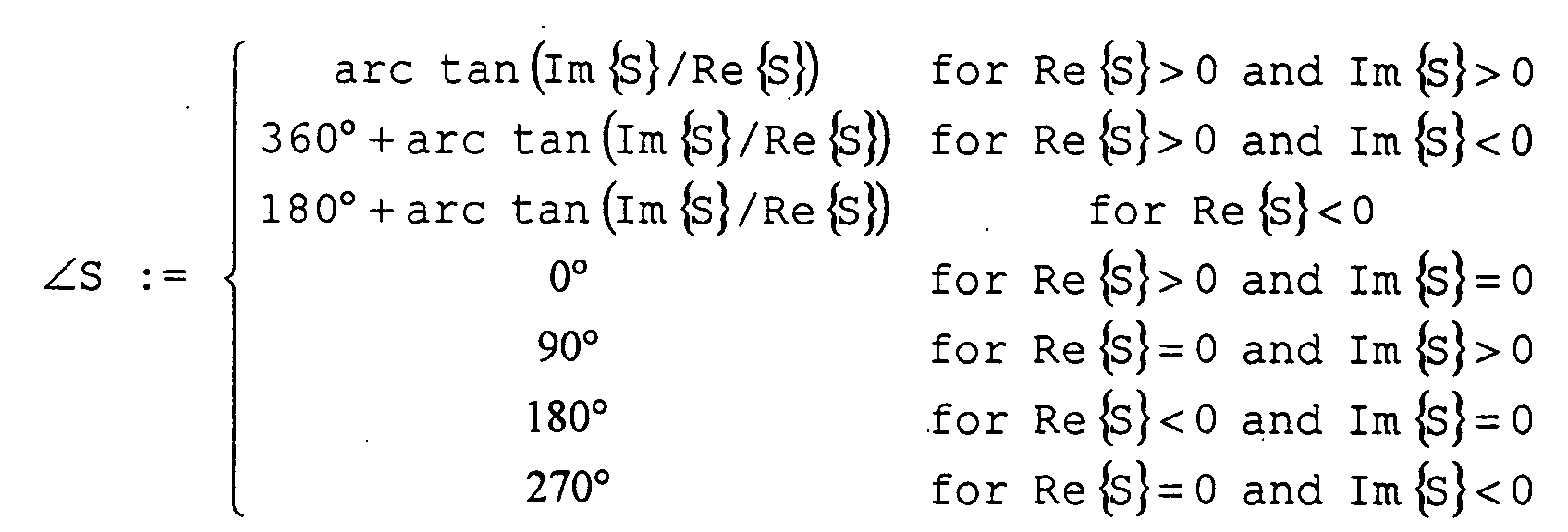
- d := |S| = |S1|/|S2|
- is the amplitude ratio of the two complex signals S1 and S2,
- arc(S) := arc(S1)-arc(S2) [deg]
- is the phase of the ratio S,
- I := Re{S} = d·cos[arc(S)]
- denotes the inphase signal of the ratio S,
- Q := Im{S} = d·sin[arc(S)]
- denotes the quadrature signal of the ratio S,
- j := -1
- is the imaginary unit, and
- e ≈ 2.718281828
- is the Euler constant.
| Port Number Index (n or m) | Reference Sign in Fig. 1 | Reference Sign in Fig. 4 |
| 1 | 102a | 401a |
| 2 | 102e | 401b |
| 3 | 102b | 401c |
| 4 | 102c | 401d |
| 5 | 102d | 401e |
- S :=
- [S1,S2,S3,S4,S5]T ∈ C5 [
- P :=
- [P1,P2,P3,P4,P5]T ∈ R5 [W] denotes the power vector,
- T :=
- is the transfer matrix, and

- 'H'
- denotes the complex conjugate transpose operation (Hermitian transpose).










| No | Failure |
| 100 | block diagram showing a general overview of the five-port structure comprising three power detectors for the detection of three power values P3, P4 and P5 (according to the state of the art) applied to the proposed topology of Fig. 4 (according to the preferred embodiment of the underlying invention) |
| 101a | direct current (DC) interface |
| 101b | digital signal processor (DSP) |
| 102 | five-port junction device |
| 102a | 1st port of the five-port junction device 102 |
| 102e | 2nd port of the five-port junction device 102 |
| 102b | 3rd port of the five-port junction device 102 |
| 102c | 4th port of the five-port junction device 102 |
| 102d | 5th port of the five-port junction device 102 |
| 104a | 1st power detector needed for the detection of the power P3 |
| 104b | 2nd power detector needed for the detection of the power P4 |
| 104c | 3rd power detector needed for the detection of the power P5 |
| 106a | power sensor of the 1st power detector 104a |
| 106b | power sensor of the 2nd power detector 104b |
| 106c | power sensor of the 3rd power detector 104c |
| 108a | lowpass (LP) filter of the 1st power detector 104a |
| 108b | lowpass (LP) filter of the 2nd power detector 104b |
| 108c | lowpass (LP) filter of the 3rd power detector 104c |
| 110 | passive three-port network comprising resistive components |
| 112 | non-reciprocal active circuitry comprising at least one phase shifter applied to serve as an isolation between the RF signal (S1) and the LO signal (S2) |
| 112a | 1st phase shifter of the non-reciprocal active circuitry 112 providing a phase shift 1 |
| 112b | 2nd phase shifter of the non-reciprocal active circuitry 112 providing a phase shift 2 |
| 112c | 3rd phase shifter of the non-reciprocal active circuitry 112 providing a phase shift 3 := 1 - 2 - 180° (or: phase shift of 180° obtained by using two phase shifters 112a and 112b providing a phase shift 1 and a phase shift 2 := 1 -180°) |
| 114 | passive four-port network comprising resistive components |
| 114a | passive power divider included in the passive four-port network 114 |
| 114b | passive three-port network comprising resistive components included in the passive four-port network 114 |
| 200 | block diagram of a circuitry providing an isolation between the RF and LO signal for a five-port junction by means of active devices (according to the state of the art) |
| 300 | topology providing an isolation between the RF signal (S1) and the LO signal (S2) for a four-port by means of passive devices (according to the state of the art) |
| 302a | passive power divider for the RF signal (S1) |
| 302b | passive power divider for the LO signal (S2) |
| 400 | topology of the proposed five-port junction device comprising three phase shifters and four passive components in order to enable a splitting and combining of the RF and LO signal (according to the preferred embodiment of the underlying invention) |
| 401a | port #1 of the five-port junction device 400 |
| 401b | port #2 of the five-port junction device 400 |
| 401c | port #3 of the five-port junction device 400 |
| 401d | port #4 of the five-port junction device 400 |
| 401e | port #5 of the five-port junction device 400 |
| 402a | 1st passive three-port network comprising resistive components |
| 402b | 2nd passive three-port network comprising resistive components |
| 402c | 3rd passive three-port network comprising resistive components |
| 500 | possible network realization of the proposed topology 400 using resistive three-ports in order to enable a splitting and combining of the RF and LO signal |
| 600 | topology of an analog circuitry (a DC amplifier network), in which the nodes P3, P4 and P5 shall be connected with the ports 401c, 401d and 401e in the network realization 500, respectively, in order to obtain I/Q output signals with the aid of analog means without needing any means for performing a digital signal processing |
| 602a | 1st amplifier (gain: g1) used for amplifying the detected power value P3 |
| 602b | 2nd amplifier (gain: g2) used for amplifying the detected power value P3 |
| 602c | 3rd amplifier (gain: g3) used for amplifying the detected power value P0 |
| 602d | 4th amplifier (gain: g4) used for amplifying the detected power value P0 |
| 602e | 5th amplifier (gain: g5) used to obtain the inphase (I) value of a received signal at the output port of said analog circuitry 600 |
| 602f | 6th amplifier (gain: g6) used to obtain the quadrature (Q) value of a received signal at the output port of said analog circuitry 600 |
| 604a | 1st summation element having one inverting input and one non-inverting input |
| 604b | 2nd summation element having one inverting input and one non-inverting input |
| 604c | 3rd summation element having one inverting input and one non-inverting input |
| 604d | 4th summation element having one inverting input and one non-inverting input |
| 700 | constellation points of a simulated 5 GHz application using a 20 MHz QPSK signal, wherein the values of the employed active elements correspond to a JFET GaAs process |
Claims (21)
- A five-port junction device used for the processing of modulated RF signals in a mobile radio receiver, wherein said five-port junction device (102) comprises:whereinat least two RF input ports (401a+b) for two RF input signals (S1 and S2),at least three output ports (401c-e) for output signals representing three detected power levels (P3, P4 and P5),two passive N-port networks (114 and 402b) connected to each other by a non-reciprocal circuitry (112a-c and 402a+c), wherein each of said passive N-port networks (114 and 402b) is connected to one of said RF input ports (401a+b), respectively,at least three power detectors (104a-c) for detecting the respective power levels (P3, P4 and P5) of the output signals, and
said non-reciprocal circuitry (112a-c and 402a+c) comprises two branches, in which the first branch contains at least one phase shifter (112a) and the second branch contains at least two phase shifters (112b+c),
characterized in that
the first end of each particular branch is connected to the first passive N-port network (114), and the second end of each branch is connected to the second passive N-port network (402b) to provide a passive isolation of the two RF input signals (S1 and S2). - A five-port junction device according to claim 1,
characterized in that
the first passive N-port network (114) is realized as a passive four-port network. - A five-port junction device according to anyone of the claims 1 and 2,
characterized in that
the second passive N-port network (402b) is realized as a passive three-port network. - A five-port junction device according to anyone of the claims 1 to 3,
characterized in that
the first passive N-port network (114) comprises one input port (401a) for the input of a first RF input signal (S1) and two output ports (401c+d) in combination with a passive three-port network (402a) connected to said first passive N-port network (114) for the output of a signal representing the power levels P3 and P4. - A five-port junction device according to anyone of the claims 1 to 4,
characterized in that
the second passive N-port network (402b) comprises one input port (401b) for the input of a second RF input signal (S2). - A five-port junction device according to anyone of the claims 1 to 5,
characterized in that
the passive three-port network (402c) comprises one output port (401e) for the output of a signal representing the power level P5. - A five-port junction device according to anyone of the claims 1 to 6,
characterized in that
the one of the RF input ports (401b) is supplied with a RF input signal (S2) originating from a local oscillator. - A five-port junction device according to anyone of the claims 1 to 7,
characterized in that
the phase shift angles (1, 2 and 3) of three phase shifters (112a-c) satisfy the equation
in order to obtain RF input signals (S1 and S2) with opposite phases for providing an isolation of said RF input signals (S1 and S2). - A five-port junction device according to anyone of the claims 1 to 8,
characterized in that
at least one of the passive N-port networks (114 and 402a-c) is realized by means of a resistive network. - A five-port junction device according to anyone of the claims 1 to 9,
characterized in that
the analog circuitry (112a-c and 402a+c) comprises a DC amplifier network (600) being connected to at least three ports (401c-e) of said five-port junction device (102) in order to obtain the inphase (I) and quadrature (Q) component of the received RF input signal (S1). - A five-port junction device according to one of the claims 1 to 10,
characterized in that
the proposed topology of said five-port junction device (102) is applied to on-chip Monolithic Microwave Integrated Circuits (MMIC) as a part of the RF systems realized on the chip. - A five-port junction device according to claim 11,
characterized in that
the Monolithic Microwave Integrated Circuits (MMIC) are realized by means of CMOS technology. - A mobile radio receiver,
characterized in that
a five-port junction device (102) according to anyone of the claims 1 to 12 is used for a direct downconversion of a received modulated RF input signal (S1). - A mobile radio receiver according to claim 13,
characterized in that
said five-port junction device (102) is used for a direct downconversion of a received nPSK-, 2 QAM- or OFDM-modulated RF input signal (S1). - A method for supporting a direct downconversion of received modulated RF signals,
characterized in that
a mobile radio receiver comprising a five-port junction device (102) used for the processing of modulated RF signals according to anyone of the claims 1 to 14 is applied, comprising the following steps:input of two RF input signals (S1 and S2) to said five-port receiver,output of three output signals being based on linear combinations of said two RF input signals (S1 and S2), anddetection of the power levels (P3, P4 and P5) of said three output signals. - A method according to claim 15,
characterized in that
a complex linear transformation is applied to calculate the correct modulation state values of a first RF input signal (S1) represented by the inphase signal (I) and the quadrature signal (Q) of said first RF input signal (S1) on the basis of actually detected power values (P3, P4 and P5), wherein the coefficients of said complex linear transformation are calculated by comparing predefined modulation states of a second RF input signal (S2) used as a calibration signal with the actually detected power values (P3, P4 and P5). - A method for providing a calibration of the five-port junction device (102) according to anyone of the claims 1 to 12,
characterized in that
an isolation of the RF input signals (S1 and S2) is achieved by means of a phase shift of at least one of said RF input signals (S1 and S2), thereby ensuring that after having performed said phase shifts the obtained values for the phases of said RF input signals (S1 and S2) are different. - A method according to claim 17,
characterized in that
three phase shifts are performed using the phase shift angles (1, 2 and 3) of three phase shifters (112a-c) satisfying the equation
in order to obtain RF input signals (S1 and S2) with opposite phases for providing an isolation of said RF input signals (S1 and S2). - A mobile telecommunications device,
wherein
a mobile radio receiver according to anyone of the claims 13 and 14 is applied. - A mobile telecommunications device,
wherein
a method for a direct downconversion of received modulated RF signals according to anyone of the claims 15 and 16 is employed. - A mobile telecommunications device,
comprising a mobile radio receiver using a five-port junction device (102) according to anyone of the claims 1 to 12,
wherein
a method for a calibration of said five-port junction device (102) is applied according to anyone of the claims 17 and 18.
Priority Applications (2)
| Application Number | Priority Date | Filing Date | Title |
|---|---|---|---|
| DE2001607682 DE60107682T2 (en) | 2001-09-21 | 2001-09-21 | Five-port receiver with passive isolation |
| EP20010122741 EP1296458B1 (en) | 2001-09-21 | 2001-09-21 | Five-port receiver with passive isolation |
Applications Claiming Priority (1)
| Application Number | Priority Date | Filing Date | Title |
|---|---|---|---|
| EP20010122741 EP1296458B1 (en) | 2001-09-21 | 2001-09-21 | Five-port receiver with passive isolation |
Publications (2)
| Publication Number | Publication Date |
|---|---|
| EP1296458A1 true EP1296458A1 (en) | 2003-03-26 |
| EP1296458B1 EP1296458B1 (en) | 2004-12-08 |
Family
ID=8178691
Family Applications (1)
| Application Number | Title | Priority Date | Filing Date |
|---|---|---|---|
| EP20010122741 Expired - Lifetime EP1296458B1 (en) | 2001-09-21 | 2001-09-21 | Five-port receiver with passive isolation |
Country Status (2)
| Country | Link |
|---|---|
| EP (1) | EP1296458B1 (en) |
| DE (1) | DE60107682T2 (en) |
Cited By (1)
| Publication number | Priority date | Publication date | Assignee | Title |
|---|---|---|---|---|
| CN104202033A (en) * | 2014-09-17 | 2014-12-10 | 王少夫 | Distributive correlator |
Citations (3)
| Publication number | Priority date | Publication date | Assignee | Title |
|---|---|---|---|---|
| US4427936A (en) * | 1981-06-22 | 1984-01-24 | Microwave Development Labs | Reflection coefficient measurements |
| EP0957614A1 (en) * | 1998-05-14 | 1999-11-17 | Sony International (Europe) GmbH | N-port demodulator for PSK or QAM signals |
| EP1067675A1 (en) * | 1999-07-08 | 2001-01-10 | Sony International (Europe) GmbH | Calibration of a N-port receiver |
-
2001
- 2001-09-21 EP EP20010122741 patent/EP1296458B1/en not_active Expired - Lifetime
- 2001-09-21 DE DE2001607682 patent/DE60107682T2/en not_active Expired - Lifetime
Patent Citations (3)
| Publication number | Priority date | Publication date | Assignee | Title |
|---|---|---|---|---|
| US4427936A (en) * | 1981-06-22 | 1984-01-24 | Microwave Development Labs | Reflection coefficient measurements |
| EP0957614A1 (en) * | 1998-05-14 | 1999-11-17 | Sony International (Europe) GmbH | N-port demodulator for PSK or QAM signals |
| EP1067675A1 (en) * | 1999-07-08 | 2001-01-10 | Sony International (Europe) GmbH | Calibration of a N-port receiver |
Cited By (1)
| Publication number | Priority date | Publication date | Assignee | Title |
|---|---|---|---|---|
| CN104202033A (en) * | 2014-09-17 | 2014-12-10 | 王少夫 | Distributive correlator |
Also Published As
| Publication number | Publication date |
|---|---|
| DE60107682D1 (en) | 2005-01-13 |
| DE60107682T2 (en) | 2005-12-15 |
| EP1296458B1 (en) | 2004-12-08 |
Similar Documents
| Publication | Publication Date | Title |
|---|---|---|
| JP4064473B2 (en) | n-port direct receiver | |
| US6823181B1 (en) | Universal platform for software defined radio | |
| JP3982662B2 (en) | Reception method and high-frequency signal receiver | |
| US7092687B2 (en) | Five-port topology for direct down-conversion | |
| EP1172927B1 (en) | Quadrature demodulator using power sensors | |
| US6507733B1 (en) | Three port junction receiver | |
| US6748203B1 (en) | Three port structure with modulated LO signal | |
| EP1296458B1 (en) | Five-port receiver with passive isolation | |
| US6999528B2 (en) | I/Q demodulator device with three power detectors and two A/D converters | |
| US6704562B1 (en) | N-port receiver with RF/LO isolation | |
| US6539215B1 (en) | Down converter and demodulator using a three port junction | |
| EP0957614A1 (en) | N-port demodulator for PSK or QAM signals | |
| US7323950B2 (en) | Balanced hybrid coupler network | |
| US6714602B1 (en) | Demodulator and receiver | |
| EP1398872B1 (en) | Adaptive autocalibration method for the quadrature demodulator of a five-port receiver | |
| EP1376852B1 (en) | I/Q Demodulator based on six-port circuit topologies for mobile receivers | |
| EP0926812A1 (en) | Six-port junction device | |
| EP0957573A1 (en) | Five-port junction device |
Legal Events
| Date | Code | Title | Description |
|---|---|---|---|
| PUAI | Public reference made under article 153(3) epc to a published international application that has entered the european phase |
Free format text: ORIGINAL CODE: 0009012 |
|
| AK | Designated contracting states |
Kind code of ref document: A1 Designated state(s): AT BE CH CY DE DK ES FI FR GB GR IE IT LI LU MC NL PT SE TR |
|
| AX | Request for extension of the european patent |
Extension state: AL LT LV MK RO SI |
|
| 17P | Request for examination filed |
Effective date: 20030430 |
|
| 17Q | First examination report despatched |
Effective date: 20030630 |
|
| AKX | Designation fees paid |
Designated state(s): DE FR GB |
|
| GRAP | Despatch of communication of intention to grant a patent |
Free format text: ORIGINAL CODE: EPIDOSNIGR1 |
|
| GRAS | Grant fee paid |
Free format text: ORIGINAL CODE: EPIDOSNIGR3 |
|
| GRAA | (expected) grant |
Free format text: ORIGINAL CODE: 0009210 |
|
| AK | Designated contracting states |
Kind code of ref document: B1 Designated state(s): DE FR GB |
|
| REG | Reference to a national code |
Ref country code: GB Ref legal event code: FG4D |
|
| REG | Reference to a national code |
Ref country code: IE Ref legal event code: FG4D |
|
| REF | Corresponds to: |
Ref document number: 60107682 Country of ref document: DE Date of ref document: 20050113 Kind code of ref document: P |
|
| RAP2 | Party data changed (patent owner data changed or rights of a patent transferred) |
Owner name: SONY CORPORATION Owner name: SONY DEUTSCHLAND GMBH |
|
| PLBE | No opposition filed within time limit |
Free format text: ORIGINAL CODE: 0009261 |
|
| STAA | Information on the status of an ep patent application or granted ep patent |
Free format text: STATUS: NO OPPOSITION FILED WITHIN TIME LIMIT |
|
| 26N | No opposition filed |
Effective date: 20050909 |
|
| ET | Fr: translation filed | ||
| REG | Reference to a national code |
Ref country code: FR Ref legal event code: CA Ref country code: FR Ref legal event code: TQ |
|
| REG | Reference to a national code |
Ref country code: FR Ref legal event code: CA |
|
| REG | Reference to a national code |
Ref country code: GB Ref legal event code: 732E |
|
| PGFP | Annual fee paid to national office [announced via postgrant information from national office to epo] |
Ref country code: GB Payment date: 20110920 Year of fee payment: 11 Ref country code: DE Payment date: 20110923 Year of fee payment: 11 Ref country code: FR Payment date: 20110928 Year of fee payment: 11 |
|
| GBPC | Gb: european patent ceased through non-payment of renewal fee |
Effective date: 20120921 |
|
| REG | Reference to a national code |
Ref country code: FR Ref legal event code: ST Effective date: 20130531 |
|
| PG25 | Lapsed in a contracting state [announced via postgrant information from national office to epo] |
Ref country code: DE Free format text: LAPSE BECAUSE OF NON-PAYMENT OF DUE FEES Effective date: 20130403 Ref country code: GB Free format text: LAPSE BECAUSE OF NON-PAYMENT OF DUE FEES Effective date: 20120921 |
|
| PG25 | Lapsed in a contracting state [announced via postgrant information from national office to epo] |
Ref country code: FR Free format text: LAPSE BECAUSE OF NON-PAYMENT OF DUE FEES Effective date: 20121001 |
|
| REG | Reference to a national code |
Ref country code: DE Ref legal event code: R119 Ref document number: 60107682 Country of ref document: DE Effective date: 20130403 |