EP1296424A2 - Semiconductor laser device with a diffraction grating and semiconductor laser module - Google Patents
Semiconductor laser device with a diffraction grating and semiconductor laser module Download PDFInfo
- Publication number
- EP1296424A2 EP1296424A2 EP02252768A EP02252768A EP1296424A2 EP 1296424 A2 EP1296424 A2 EP 1296424A2 EP 02252768 A EP02252768 A EP 02252768A EP 02252768 A EP02252768 A EP 02252768A EP 1296424 A2 EP1296424 A2 EP 1296424A2
- Authority
- EP
- European Patent Office
- Prior art keywords
- semiconductor laser
- mount
- laser element
- laser device
- thin film
- Prior art date
- Legal status (The legal status is an assumption and is not a legal conclusion. Google has not performed a legal analysis and makes no representation as to the accuracy of the status listed.)
- Withdrawn
Links
Images






Classifications
-
- H—ELECTRICITY
- H01—ELECTRIC ELEMENTS
- H01S—DEVICES USING THE PROCESS OF LIGHT AMPLIFICATION BY STIMULATED EMISSION OF RADIATION [LASER] TO AMPLIFY OR GENERATE LIGHT; DEVICES USING STIMULATED EMISSION OF ELECTROMAGNETIC RADIATION IN WAVE RANGES OTHER THAN OPTICAL
- H01S5/00—Semiconductor lasers
- H01S5/02—Structural details or components not essential to laser action
- H01S5/024—Arrangements for thermal management
- H01S5/02476—Heat spreaders, i.e. improving heat flow between laser chip and heat dissipating elements
- H01S5/02484—Sapphire or diamond heat spreaders
-
- H—ELECTRICITY
- H01—ELECTRIC ELEMENTS
- H01S—DEVICES USING THE PROCESS OF LIGHT AMPLIFICATION BY STIMULATED EMISSION OF RADIATION [LASER] TO AMPLIFY OR GENERATE LIGHT; DEVICES USING STIMULATED EMISSION OF ELECTROMAGNETIC RADIATION IN WAVE RANGES OTHER THAN OPTICAL
- H01S5/00—Semiconductor lasers
- H01S5/02—Structural details or components not essential to laser action
- H01S5/0206—Substrates, e.g. growth, shape, material, removal or bonding
- H01S5/0213—Sapphire, quartz or diamond based substrates
-
- H—ELECTRICITY
- H01—ELECTRIC ELEMENTS
- H01S—DEVICES USING THE PROCESS OF LIGHT AMPLIFICATION BY STIMULATED EMISSION OF RADIATION [LASER] TO AMPLIFY OR GENERATE LIGHT; DEVICES USING STIMULATED EMISSION OF ELECTROMAGNETIC RADIATION IN WAVE RANGES OTHER THAN OPTICAL
- H01S5/00—Semiconductor lasers
- H01S5/02—Structural details or components not essential to laser action
- H01S5/022—Mountings; Housings
- H01S5/0225—Out-coupling of light
- H01S5/02251—Out-coupling of light using optical fibres
-
- H—ELECTRICITY
- H01—ELECTRIC ELEMENTS
- H01S—DEVICES USING THE PROCESS OF LIGHT AMPLIFICATION BY STIMULATED EMISSION OF RADIATION [LASER] TO AMPLIFY OR GENERATE LIGHT; DEVICES USING STIMULATED EMISSION OF ELECTROMAGNETIC RADIATION IN WAVE RANGES OTHER THAN OPTICAL
- H01S5/00—Semiconductor lasers
- H01S5/02—Structural details or components not essential to laser action
- H01S5/022—Mountings; Housings
- H01S5/023—Mount members, e.g. sub-mount members
- H01S5/02325—Mechanically integrated components on mount members or optical micro-benches
-
- H—ELECTRICITY
- H01—ELECTRIC ELEMENTS
- H01S—DEVICES USING THE PROCESS OF LIGHT AMPLIFICATION BY STIMULATED EMISSION OF RADIATION [LASER] TO AMPLIFY OR GENERATE LIGHT; DEVICES USING STIMULATED EMISSION OF ELECTROMAGNETIC RADIATION IN WAVE RANGES OTHER THAN OPTICAL
- H01S5/00—Semiconductor lasers
- H01S5/02—Structural details or components not essential to laser action
- H01S5/022—Mountings; Housings
- H01S5/0233—Mounting configuration of laser chips
- H01S5/0234—Up-side down mountings, e.g. Flip-chip, epi-side down mountings or junction down mountings
-
- H—ELECTRICITY
- H01—ELECTRIC ELEMENTS
- H01S—DEVICES USING THE PROCESS OF LIGHT AMPLIFICATION BY STIMULATED EMISSION OF RADIATION [LASER] TO AMPLIFY OR GENERATE LIGHT; DEVICES USING STIMULATED EMISSION OF ELECTROMAGNETIC RADIATION IN WAVE RANGES OTHER THAN OPTICAL
- H01S5/00—Semiconductor lasers
- H01S5/02—Structural details or components not essential to laser action
- H01S5/024—Arrangements for thermal management
- H01S5/02407—Active cooling, e.g. the laser temperature is controlled by a thermo-electric cooler or water cooling
- H01S5/02415—Active cooling, e.g. the laser temperature is controlled by a thermo-electric cooler or water cooling by using a thermo-electric cooler [TEC], e.g. Peltier element
-
- H—ELECTRICITY
- H01—ELECTRIC ELEMENTS
- H01S—DEVICES USING THE PROCESS OF LIGHT AMPLIFICATION BY STIMULATED EMISSION OF RADIATION [LASER] TO AMPLIFY OR GENERATE LIGHT; DEVICES USING STIMULATED EMISSION OF ELECTROMAGNETIC RADIATION IN WAVE RANGES OTHER THAN OPTICAL
- H01S5/00—Semiconductor lasers
- H01S5/10—Construction or shape of the optical resonator, e.g. extended or external cavity, coupled cavities, bent-guide, varying width, thickness or composition of the active region
- H01S5/12—Construction or shape of the optical resonator, e.g. extended or external cavity, coupled cavities, bent-guide, varying width, thickness or composition of the active region the resonator having a periodic structure, e.g. in distributed feedback [DFB] lasers
- H01S5/1203—Construction or shape of the optical resonator, e.g. extended or external cavity, coupled cavities, bent-guide, varying width, thickness or composition of the active region the resonator having a periodic structure, e.g. in distributed feedback [DFB] lasers over only a part of the length of the active region
-
- H—ELECTRICITY
- H10—SEMICONDUCTOR DEVICES; ELECTRIC SOLID-STATE DEVICES NOT OTHERWISE PROVIDED FOR
- H10W—GENERIC PACKAGES, INTERCONNECTIONS, CONNECTORS OR OTHER CONSTRUCTIONAL DETAILS OF DEVICES COVERED BY CLASS H10
- H10W72/00—Interconnections or connectors in packages
- H10W72/50—Bond wires
- H10W72/551—Materials of bond wires
- H10W72/552—Materials of bond wires comprising metals or metalloids, e.g. silver
- H10W72/5522—Materials of bond wires comprising metals or metalloids, e.g. silver comprising gold [Au]
Definitions
- the present invention relates to a semiconductor laser device and a semiconductor laser module provided with a semiconductor laser element for outputting a laser beam having a plurality of oscillation longitudinal modes.
- WDM systems support transmission volumes 100 times larger than the capacity of conventional fiber optic communications by superimposing a plurality of optical signals at different wavelengths on a single fiber.
- Current WDM systems are capable of long distance transmissions by performing optical amplification with an erbium-doped fiber amplifier (EDFA) or Raman amplifier.
- EDFA is an optical fiber amplifier with erbium added.
- a Raman amplifier is an amplifier capable of directly amplifying signal light by using an already laid optical fiber as an amplifying medium and introducing amplifying light via using stimulated Raman scattering.
- the interval between repeaters must be small due to inefficient amplification. With more repeaters, costs increase. Therefore, to be able to increase the interval between repeaters, one can either increase the output of a semiconductor laser device used for a signal light source and/or improve the amplifying capacity of the repeater.
- a semiconductor laser element capable of outputting a laser beam of 250 mW or more is used for EDFA excitation. This higher power level requires high reliability from the semiconductor laser devices.
- a thermistor for measuring the temperature of a semiconductor laser element is often set nearby the semiconductor laser element so that the temperature of the semiconductor laser element can be controlled by an electrothermal element such as a Peltier element.
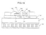
- Fig. 18 is a front view showing a schematic configuration of a conventional semiconductor laser device.
- a submount 102 formed by AlN having an insulating property and a high heat conductivity is set on a carrier 101 formed by CuW.
- a semiconductor laser element 103 for outputting a laser beam of a predetermined wavelength is set on the submount 102.
- a submount 104 formed by AlN is set on the carrier 101 and, a thermistor 105 for measuring the temperature of the semiconductor laser element 103 is set on the submount 104.
- the semiconductor laser element 103 and the submount 102 are joined to each other through a metallic thin film 102a.
- the metallic thin film 102a contains layers of Ti, Pt, and Au at thicknesses of 60 nm, 200 nm, and 600 nm respectively.
- the semiconductor laser element 103 and submount 102 are joined on the metallic thin film 102 by a solder material such as AuSn.
- the thermistor 105 and submount 104 are also joined through a metallic thin film 104a.
- the face of the semiconductor laser element 103 to be joined with the submount 102 serves as a p-side electrode and the upper face serves as an n-side electrode.
- the semiconductor laser element 103 is set so that the active layer serving as a main heat generating source is present at the p-side electrode side and located nearby the submount 102.
- the n-side electrode is connected to a negative electrode by an Au wire 106a.
- the p-side electrode is connected to the carrier 101 at the positive electrode side through the metallic thin film 102a and an Au wire 106b.
- Submount 102 secures the insulation of the semiconductor laser element 103 and functions as a heat sink of the semiconductor laser element 103.
- the bottom is joined to a CuW base 110 by AuSn solder.
- the base 110 is set on a Peltier element 120.
- the Peltier element 120 is controlled by a temperature control section (not illustrated) correspondingly to the temperature detected by the thermistor 105.
- the temperature of the semiconductor laser element 103 is controlled by the thermistor 105, Peltier element 120, and the temperature control section.
- the thermistor 105 is also insulated from the carrier 101 by the submount 104 to detect the temperature of the semiconductor laser element 103 through the submount 102, carrier 101, and submount 104, each of which has a high heat conductivity.
- the heat generated in the semiconductor laser element 103 is conducted to the thermistor 105 through the metallic thin film 102a, submount 102, metallic thin film 102b, carrier 101, metallic thin film 104b, submount 104, and metallic thin film 104a in order.
- the heat conducting distance degrades overall operations as the actual temperature detection of the semiconductor laser element 103 is delayed.
- the generated heat passes through the metallic thin films 102a, 102b, 104b, and 104a that are joined to each other by four AuSn solder joints.
- the AuSn solder joints are used for the junction they respectively have a large heat joints resistance, and so the heat resistance of the above heat conducting path is increased.
- the temperature control accuracy is also deteriorated.
- the oscillation wavelength of the semiconductor laser element 103 is prone to becoming unstable due to heat generated at high powers, and the system optical output and service life are deteriorated.
- a semiconductor laser element that includes a diffraction grating.
- laser elements include those disclosed in Japanese Patent Application No. 2000-323118, Japanese Patent Application No. 2001-134545, and Japanese Patent Application No. 2002-228669 filed on 10/28/2000, 5/1/2001 and 7/27/2001 respectively in the Japanese Patent Office, the entire contents of which being incorporated herein by reference.
- These types of laser elements are configured to output a laser beam with a plurality of oscillation longitudinal modes at or below a threshold at which stimulated Brillouin scattering occurs.
- These types of laser elements suffer unique degradations in performance due to temperature effects. Specifically, the temperature of a semiconductor laser element rises with increases in the current injected into the laser element's active layer.
- This temperature increase causes the refractive index of the diffraction grating layer to change.
- This change in refractive index causes the selection wavelength of the diffraction grating to shift such that the desired central output wavelength cannot be obtained. Therefore, in the case of an iGM laser that has a diffraction grating, the present inventors determined that it is desirable to go beyond conventional measures to accommodate the heat producing high powers.
- This invention provides a semiconductor iGM laser device and a semiconductor iGM laser module capable of preventing the optical output and service life of a high output semiconductor laser element from deteriorating the way they do with conventional device. This is achieved by using new materials in such devices and modules to enable a reduction in the number of interfaces between a laser element and a temperature measuring device, as well as a reduction in the number of interfaces between a laser element and a Peltier module. In addition, performance is enhanced by improving the uniformity of voltage drop of the semiconductor laser element in the resonator length direction by distributing driving currents along a length of the resonator cavity.
- the first configuration of the present invention includes a semiconductor laser device having a first mount, a second mount formed by a heat sink having a heat conductivity of 500 W/(m*K) or more and set onto the first mount, and a semiconductor laser element joined on to the second mount through a multi-layer film including a gold thin film.
- the semiconductor laser device also includes a thermistor set on a third mount which is joined onto the first mount through a multi-layer film, including a gold thin film.
- the second configuration of the present invention includes a semiconductor laser device having a first mount, a second mount formed by a heat sink having a heat conductivity of 500 W/(m*K) or more and set onto the first mount, and a semiconductor laser element joined on to the second mount through a multi-layer film, including a gold thin film.
- the semiconductor laser device also includes a thermistor joined directly onto the first mount through a multi-layer film, including a gold thin film.
- the third configuration of the present invention includes a semiconductor laser device having a first mount, a second mount formed by a heat sink having a heat conductivity of 500 W/(m*K) or more and set onto the first mount, and a semiconductor laser element joined on to the second mount through a multi-layer film, including a gold thin film.
- the semiconductor laser device also includes a thermistor also joined onto the second mount through a multi-layer film, including a gold thin film.
- a fourth configuration of the present invention includes a semiconductor laser module having the semiconductor laser device according to any one of the first to third aspects, a temperature controlling element for controlling the temperature of the above semiconductor laser element in accordance with the temperature output from the above temperature measuring element, and a fourth mount set onto the above temperature controlling element, in which the above semiconductor laser device is set onto the fourth mount and the above semiconductor laser element is temperature controlled through the fourth mount.
- the present invention has been conceived in order to solve the above described problems of conventional devices and modules regarding heat dissipation and thermally-induced laser performance degradations.
- Embodiments of a semiconductor laser device and a semiconductor laser module of the present invention are described below in detail by referring to the accompanying drawings.
- the present invention is tailored for a "semiconductor laser device" configured to output a laser beam with a plurality of oscillation longitudinal modes as disclosed in Japanese Patent Application No. 2000-323118, Japanese Patent Application No. 2001-134545, and Japanese Patent Application No. 2001-228669, the entire contents of each of which being incorporated herein by reference.
- Fig. 1 is a perspective sectional view showing a schematic configuration of a semiconductor laser element in each of this invention's embodiments.
- Fig. 2 is a longitudinal sectional view of the semiconductor laser element shown in Fig. 1.
- Fig. 3 is a sectional view of the semiconductor laser element shown in Fig. 2, taken along the line A-A in Fig. 2.
- Fig. 1 is a perspective sectional view showing a schematic configuration of a semiconductor laser element in each of this invention's embodiments.
- Fig. 2 is a longitudinal sectional view of the semiconductor laser element shown in Fig. 1.
- Fig. 3 is a sectional view of the semiconductor laser element shown in Fig. 2, taken along the line A-A in Fig. 2.
- Fig. 1 is a perspective sectional view showing a schematic configuration of a semiconductor laser element in each of this invention's embodiments.
- Fig. 2 is a longitudinal sectional view of the semiconductor laser element shown in Fig. 1.
- Fig. 3 is a sectional view
- the semiconductor laser element 20 is constituted by forming an n-InP buffer layer 2 also serving as a buffer layer made of n-InP and a lower clad layer, GRIN-SCH-MQW (Graded Index Separate Confinement Heterostructure Multi Quantum Well) active layer 3 having a compressive strain, a p-InP spacer layer 4, a p-InP clad layer 6, and an InGaAsP cap layer 7 on the surface of an n-InP substrate 1 in order.
- GRIN-SCH-MQW Gram Index Separate Confinement Heterostructure Multi Quantum Well
- a reflection film 14 having a high light reflectance of 80% or more is formed on the light reflection edge of the semiconductor laser element 20 serving as one end face of the element 20 in its longitudinal direction and an emission side reflection film 15 having a low light reflectance of 2% or less, preferably a low light reflectance of 1% or less is formed on the light emission edge of the element 20 serving as its other end face.
- the light generated in the GRIN-SCH-MQW active layer 3 of an optical resonator formed by the reflection film 14 and the emission side reflection film 15 is reflected from the reflection film 14 and emitted as a laser beam through the emission side reflection film 15.
- the semiconductor laser element 20 has a diffraction grating 13 made of p-InGaAsP periodically formed in the p-InP spacer layer 4. Particularly in this case, it is assumed that the diffraction grating 13 extends up to 100 ⁇ m from the emission side reflection film 15 so that a laser beam having a central wavelength of 1.48 ⁇ m is selected out of laser beams generated in the gain area of the GRIN-SCH-MQW active layer 3 and is formed by having a film thickness of 20 nm and at a pitch of approximately 220 nm. It is preferable that the diffraction grating 13 is formed in contact with the emission side reflection film 15.
- the diffraction grating 13 is also possible to form the diffraction grating 13 separately from the emission side reflection film 15 in a range in which the grating 13 shows its function, that is, in a range of 20 to 100 ⁇ m. Moreover, it is allowed that the diffraction grating 13 is left at the reflection film 14 side due to the fluctuation of the cleavage position of the semiconductor laser element 20 caused in fabrication of the semiconductor laser element 20.
- the upper portion of the n-InP buffer layer 2, GRIN-SCH-MQW active layer 3, and p-InP spacer layer 4 including the above diffraction grating 13 are formed like a mesa stripe and the both sides of the mesa stripe are embedded by a p-InP layer 8 and an n-InP blocking layer 9 respectively formed as a current blocking layer.
- a p-side electrode 10 is formed on the surface of the InGaAsP cap layer 7 and an n-side electrode 11 is formed on the back of the n-InP substrate 1.
- the oscillation wavelength o is set to 1,100 to 1,550 nm and the resonator length L is set in an inclusive range of 800 through 3,200 ⁇ m.
- the interval ⁇ between longitudinal modes becomes approximately 0.39nm when the resonator length L is equal to 800 ⁇ m and becomes approximately 0.1 nm when the length L is equal to 3,200 ⁇ m. That is, as the resonator length L is increased, the longitudinal-mode interval ⁇ decreases and a selection condition for oscillating a laser beam of a single longitudinal mode becomes more severe.
- the diffraction grating 13 selects a longitudinal mode in accordance with its center selective wavelength characteristic.
- Fig. 4 is a graph for explaining a selective wavelength characteristic by the diffraction grating 13.
- the selective wavelength characteristic by the diffraction grating 13 is shown as the illustrated oscillation wavelength spectrum 30.
- the semiconductor laser element 20 is designed so that a plurality of oscillation longitudinal modes are present in a wavelength selection characteristic shown by the half-width ⁇ h of the oscillation wavelength spectrum 30.
- a semiconductor laser device having the resonator length L cannot be used because single longitudinal-mode oscillation is difficult.
- the semiconductor laser element 20 outputs a laser beam including a plurality of oscillation longitudinal modes in the half-width ⁇ h of an oscillation wavelength spectrum by positively setting the resonator length L to 800 ⁇ m or more.
- three oscillation longitudinal modes 31 to 33 are included in the half-width ⁇ h of an oscillation wavelength spectrum.
- Figs. 5A and 5B are illustrations for explaining profiles of a laser beam having a single longitudinal mode and a laser beam having a plurality of oscillation longitudinal modes.
- the semiconductor laser element 20 has the profile shown in Fig. 5B and makes it possible to obtain a high laser output having a low peak value.
- Fig. 5A is the profile of a semiconductor laser device having a single longitudinal mode when obtaining the same laser output, in which a high peak value is present.
- the semiconductor laser element 20 when using the semiconductor laser element 20 as the exciting light source of a Raman amplifier, it is preferable to increase the exciting light output power in order to increase the Raman gain.
- the peak value of the power is too high, degradation due to stimulated Brillouin scattering occurs and noise increases.
- the semiconductor laser element 20 is configured emit a laser beam in a plurality of oscillation longitudinal modes by suppressing a peak value to the threshold value Pth of stimulated Brillouin scattering or less as shown in Fig. 5B. This results in laser output substantially the same as the case of the profile shown in Fig. 5A.
- the wavelength interval (mode interval) ⁇ between the oscillation longitudinal modes 31 to 33 is set to 0.1 nm or more. This is because the probability of simulated Brillouin scattering occurrence rises if the mode interval ⁇ is equal to or less than 0.1 nm when using the semiconductor laser element 20 as the exciting light source of a Raman amplifier.
- the above resonator length L is set to 3,200 ⁇ m or less in accordance with the above expression of the mode interval ⁇ .
- the number of oscillation longitudinal modes included in the half-width ⁇ h of the oscillation wavelength spectrum 30 is two or more.
- the semiconductor laser element 20 set in the semiconductor laser device is configured to stably produce a high laser output without causing stimulated Brillouin scattering. This is because the diffraction grating 13 and the resonator length L are set so that two or more oscillation longitudinal modes are included in the half-width of an oscillation wavelength spectrum.
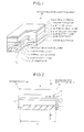
- Fig. 6A is an illustration showing a front view of the semiconductor laser device of the first embodiment and its control system.
- a submount 42 made of diamond having an insulating characteristic and a high heat conductivity is formed on a carrier 41 made of CuW and the above semiconductor laser element 20 is formed on the submount 42.
- a submount 44 made of AlN is formed on the carrier 41 and a thermistor 45 for measuring the temperature of the semiconductor laser element 20 is formed on the submount 44.
- An optical monitor (not shown) may also be mounted on the carrier 41.
- the semiconductor laser element 20 is joined with the submount 42 through a metallic thin film 42a.
- the submount 42 is joined with the carrier 41, through a metallic film 42b.
- the junction face of the semiconductor laser element 20 with the submount 42 is a p-side electrode and the upper face of the element 20 is an n-side electrode. Since the active layer of the semiconductor laser element 20 is the main heat generating source, this layer is configured to be the p-electrode and is placed on the submount 42.
- the lower portion of the carrier 41 is joined to a base 110 made of CuW by AuSn solder 42d.
- the base 110 is formed on a Peltier element 120.
- Figure 6B is a top view of the first embodiment.
- Metallic thin films 42a - 42c are patterned and formed so as to be insulated from each other.
- the metallic thin films 42a - 42c are formed as a structure in which Ti, Pt, and Au are layered in order from the carrier 41 side with thicknesses of 60mn, 200mn, and 5,000mn, respectively.
- the p-side electrode of the semiconductor laser element 20 at the outside is joined so as to face the submount 41 and the n-side electrode serves as an upper face.
- the p-side electrode of the semiconductor laser element 20 and submount 41 are electrically connected to each other through the metallic thin film 42a and Au wire 47.
- the n-side electrode of the semiconductor laser element 20 and metallic thin film 42c, which is mounted on submount 41 via electrode mount 42f, are electrically connected to each other through a plurality of wires 48.
- the metallic thin film 42a serves as a negative electrode of the semiconductor laser element 20 and the metallic thin film 42c serves as a positive electrode of the semiconductor laser element 20.
- a plurality of wires 48 are used to electrically connect the inside electrode and the metallic thin film 42c of the semiconductor laser element 20 to each other so as to increase the current carrying area. This enables a reduction in the resistance value produced along the wiring portion and reduces a voltage drop along the wiring portion. This reduction of voltage drop contributes to suppression of heat produced and increases the power ratio used for the laser beam output.
- By making the joints between the wires 48 almost equal in interval it is possible to disperse current distribution along the length of the semiconductor laser 20 and decrease the non-uniformity of voltage drop along the length. This prevents both the optical output and the service life of the device from deteriorating.
- the submount 42 is formed from polycrystal diamond synthesized through chemical vapor deposition (CVD). The method for sizing the diamond submount is described below.
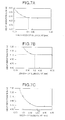
- Figs. 7A to 7C are illustrations of calculated data showing the relation between size and heat resistance of the submount 42 made of diamond.
- Fig. 7A is a graph showing the relation between thickness and heat resistance when fixing the length of the submount 42 to 2.5 mm and the width to 1.0 mm.
- Fig. 7B is a graph showing the relation between width and heat resistance when fixing the length of the submount 42 to 0.2 mm and the width to 1.0 mm.
- Fig. 7C is a graph showing the relation between width and heat resistance when fixing the length of the submount 42 to 2.5 mm and the thickness to 0.2 mm. From each graph, it is found that a heat resistance converges into a minimum value as a size increases. Therefore, in accordance with these graphs, it is possible to estimate the optimum size of a submount at which heat transference is optimized.
- Fig. 8 is a perspective view for explaining the optimum size of the submount 42.
- the thickness SH of the diamond submount 42 is set to 0.3mm, the length SL of it is set to 2.7 mm, and the width SW of it is set to 1.0 mm, resulting heat transference characteristic 1.2 times larger than the above minimum heat resistance.
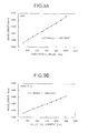
- Fig. 9A shows the injection current oscillation wavelength characteristic when using AlN for the conventional submount 102 (Fig. 18) and Fig. 9B shows the injection current oscillation wavelength characteristic when using diamond for the submount 42 of this invention.
- the graph in Fig. 9A shows that in the conventional case the oscillation wavelength shifts from approximately 1,495.5 nm to approximately 1,499.5 nm as the injection current is increased from 100 mA to 1,000 mA.
- Fig. 9B shows that the oscillation wavelength in the first embodiment shifts from approximately 1,495.5 nm to approximately 1,498.0 nm as the injection current is increased from 100 mA to 1,000 mA.
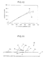
- Fig. 10 characterizes experiment data showing relations between injection current and laser beam output power when using an AlN submount 102 (Fig. 18) and a diamond submount 42.
- the continuous line 48 shows the injection current output power characteristic when using diamond for the submount 42
- the dotted line 49 shows the injection current output power characteristic when using AlN for the submount 102.
- the laser beam output power increases as the injection current increases in cases of the line 48 and line 49. However, the output power is larger in the case of line 48. That is, a larger output power for a given injection current is possible when using the diamond submount 42 compared to using the AlN submount 102.
- injection currents when the submount is made of AlN, when injection currents equal 500 mA, power output equals 159.4 mW; 900 mA of injection current results in power output equal to 264.2 mW; and when injection current equals 1200 mA, power output equals 312.2 mW.
- injection currents of 500 mA result in power outputs of 168.1 mW
- 900 mA injection currents result in power outputs of 281.7 mW
- 1200 mA injection currents result in an output power of 336.2 mW.
- a variable power source 200 applies a predetermined voltage between the n-side electrode and p-side electrode of the semiconductor laser element 20, a driving current is supplied to the semiconductor laser element 20 and, thereby, the semiconductor laser element 20 oscillates and outputs a laser beam having a desired wavelength from an active layer.
- the above driving current is detected by a current detector 201 and the detection result is further input to the temperature control section 202.
- the temperature control section 202 has a storage section 203 for holding a control function and computes a control temperature by applying the above driving current to the control function.
- the thermistor 45 is connected to the temperature control section 202 enabling the temperature control section 202 to control the current direction and level to the Peltier element 120.
- the Peltier element 120 cools the laser device and when the temperature falls below a lower threshold the Peltier element 120 heats the laser device.
- the first embodiment it is possible to reduce the shift of a selective wavelength in a diffraction grating, to improve the current pair light transformation efficiency from an injection current to a laser beam, and to effectively obtain a higher laser output for a given injection current.
- the semiconductor laser device of the second embodiment is described below. Whereas in the first embodiment a diamond submount is used for the semiconductor laser element and an AlN submount is used for the thermistor, in the second embodiment the thermistor is directly mounted on the carrier without a submount.
- Fig. 11 is an illustration showing a configuration of the semiconductor laser device of the second embodiment.
- Figs. 12A and 12B are a right side view and a top view respectively of a semiconductor laser device.
- a base on which a carrier 51 is mounted a Peltier element on which the base is mounted, and other control systems are not illustrated. Configurations and operations of these elements as described in the first embodiment discussion of Fig. 6A are applicable to the second embodiment.
- the carrier 51 is formed by AlN having a high insulation characteristic and a high heat conductivity.
- metallic thin films 52a to 52d are patterned and formed so as to be insulated from each other.
- the metallic thin films 52a to 52d are formed as a structure in which Ti, Pt, and Au are layered in order from the carrier 51 side with thicknesses of 60 nm, 200 nm, and 5,000 nm in order.
- a diamond submount 52 is formed on the carrier 51 through the metallic thin film 52b.
- a semiconductor laser element 53 is formed on the submount 52 through the metallic thin film 52e.
- the semiconductor laser element 53 is a semiconductor laser elements same as the semiconductor laser element 20.
- the submount 52 secures the insulation of the semiconductor laser element 53 and functions as the heat sink of the semiconductor laser element 53 similarly to the case of the submount 42 described for the first embodiment.
- the p-side electrode of the semiconductor laser element 53 at the active layer side is joined so as to face the submount 52 and the n-side electrode serves as an upper face.
- the p-side electrode and metallic thin film 52b of the semiconductor laser element 53 are electrically connected to each other through the metallic thin film 52e and an Au wire 56. Therefore, the metallic thin film 52e serves as a positive electrode of the semiconductor laser element 53 and the metallic thin film 52a serves as a negative electrode of the semiconductor laser element 53. Therefore, the configuration including the variable power source 200 and the current detector 201 is connected to wirings (not illustrated) extended from the metallic thin films 52 and 52b.
- a plurality of wires 55 are used to electrically connect the n-side electrode and the metallic thin film 52a of the semiconductor laser element 53 to each other so as to increase the current carrying sectional area. Thereby, it is possible to reduce a resistance value produced at a wiring portion and a voltage drop at the portion. Reduction of the voltage drop contributes to suppression of heat to be produced and increase of a power ratio only used for a laser beam output and, as a result, improves a power light transformation efficiency. By making joints between the wires 55 almost equal intervals it is possible to disperse power. Thereby, it is possible to decrease the non-uniformity of voltage drops and, as a result, prevent both optical output and service life from deteriorating.
- Bonding portions of the above wires 55 are linearly arranged in the longitudinal direction of the semiconductor laser element 53 as shown in Fig. 12B. However, it is also allowed to uniformly disperse the bonding portions on the surface of the n-side electrode of the semiconductor laser element 53. In this case, it is also possible to set the bonding portions to positions separate from the position of the active layer of the semiconductor laser element 53. It is preferable that currents are uniformly distributed via the wire 55 on the upper face of the semiconductor laser element 53, although, differing current flows are feasible as well, especially since the wires also serve as a heat sink.
- a thermistor 54 for measuring the temperature of the semiconductor laser element 53 is set on the carrier 51 through the metallic thin film 52c.
- the bottom face of the thermistor 54 serving as one electrode is joined to the metallic thin film 52c and the upper face of the thermistor 54 serving as the other electrode is electrically connected with the metallic thin film 52d through a wire 57. Therefore, the temperature control section 202 shown in Fig. 6A is connected to wirings (not illustrated) extended from the metallic thin films 52c and 52d.
- An optical monitor (not shown) may be mounted on the carrier.
- the high output semiconductor laser element 53 By setting the high output semiconductor laser element 53 so that an end face 53a of the semiconductor laser element 53 becomes almost flush with an end face of the carrier 51, it is possible to reduce the interference of a laser beam by the carrier.
- the placement of the end face 53a of the semiconductor laser element 53 cannot sufficiently receive the radiation effect by the submount 52 and, therefore, it is subjected to higher temperatures compared to other portions of the semiconductor laser element 53. For this reason, it is particularly preferable to set the thermistor 54 near the end face 53a of the semiconductor laser element 53 where the laser is emitted.
- the carrier 51 functions as the heat sink of the thermistor 54.
- the length and resistance of the heat conduction path between the semiconductor laser element 53 is reduced and the thermistor 54 can more quickly and accurately detect the actual temperature of the semiconductor laser element 53.
- the metallic thin film 52e on the submount 52 is connected with the metallic thin film 52b on the carrier 51 through the wire 56 and, a current can be carried to the p-side electrode of the semiconductor laser element 53.
- a current can be carried to the p-side electrode of the semiconductor laser element 53.
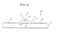
- Fig. 13 is an illustration showing another configuration of the semiconductor laser device of the second embodiment in the above case.
- Figs. 14A and 14B are a right side view and a top view of this alternative configuration.
- elements common with Figs. 11 and 12 are provided with the same symbol and so their description is omitted.
- the semiconductor laser device 50' shown in Figs. 13 and 14 is different from the semiconductor laser device in Figs. 11 and 12 in that the wire 56 is excluded and the upper face and side face of the submount 52 are covered with a metallic thin film 52f.
- the metallic thin film 52f electrically contacts with the p-side electrode of the semiconductor laser element 53 located at the upper face of the submount 52 and the metallic thin film 52b on the carrier 51.
- the semiconductor laser device of the second embodiment it is possible to obtain advantages of the first embodiment because of forming the submount 52 set between the semiconductor laser element 53 and the carrier 51 by diamond having a high heat conductivity and quickly and accurately perform the temperature control by the thermistor 54, Peltier element 120, and temperature control section 202 because the thermistor 54 is set on the carrier 51 not through a submount and thereby, the heat conduction distance from the semiconductor laser element 53 to the thermistor 54 is decreased.
- the submount 52 is formed by diamond having a high heat conductivity in the path between the Peltier element 120, base 110, carrier 51, submount 52, and semiconductor laser element 53, it is also possible to quickly and accurately perform the temperature control by the Peltier element 120.
- the semiconductor laser device of the third embodiment is described below.
- a semiconductor laser element is set on a diamond submount.
- both a semiconductor laser element and a thermistor are set on a common diamond submount.
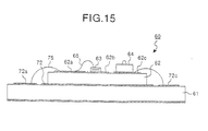
- Fig. 15 is an illustration showing a configuration of the semiconductor laser device of the third embodiment.
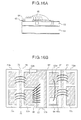
- Figs. 16A and 16B are a right side view and a top view of the semiconductor laser device.
- the structure of the semiconductor laser device of the third embodiment is described below by referring to the above three drawings.
- a base on which a carrier 61 is mounted and a Peltier element on which the base is mounted, and other control systems are not illustrated.
- configurations and operations of these elements as described in the first embodiment discussion of Fig. 6A are applicable to the third embodiment.
- the carrier 61 is formed by AlN having a high insulating characteristic and a high heat conductivity.
- Metallic thin films 72 and 72a to 72d are patterned and formed on the carrier 61 so as to be insulated from each other as shown in Figs. 16a and 16b.
- a diamond submount 62 similar to that of the first embodiment is set on the carrier 61 through the metallic thin film 72.
- Metallic thin films 62a to 62d are patterned and formed on the submount 62 so as to be insulated from each other as shown in Figs. 16a and 16b.
- a semiconductor laser element 63 is set through the metallic thin film 62b and a thermistor 64 is set through the metallic thin film 62c on the submount 62.
- the semiconductor laser element 63 is a semiconductor laser element similar to the semiconductor laser element 20 described for the first embodiment.
- the submount 62 secures the insulation of the semiconductor laser element 63 and that of the thermistor 64 and functions as a heat sink similarly to the submount 42 described for the first embodiment.
- the p-side electrode of the semiconductor laser element 63 at the active layer side is joined to the submount and the n-side electrode serves as an upper face.
- the n-side electrode of the semiconductor laser element 63 and the metallic thin film 72a on the carrier 61 are electrically connected to each other through an Au wire 65, the metallic thin film 62a, and an Au wire 75.
- the p-side electrode of the semiconductor laser element 63 and a metallic thin film 72b are electrically connected to each other through the metallic thin film 62b and an Au wire 76.
- the metallic thin film 72a serves as a negative electrode of the semiconductor laser element 63 and the metallic thin film 72b serves as a positive electrode of the semiconductor laser element 63.
- the configuration having the variable power source 200 and current detector 201 shown in Fig. 6A is connected to wirings (not illustrated) extended from the metallic thin films 72a and 72b.
- the thermistor 64 for measuring the temperature of the semiconductor laser element 63 is set on the carrier 61 through the metallic thin film 62c.
- the thermistor 64 bottom face serving as one electrode is joined to the metallic thin film 62c and the upper face serving as the other electrode is electrically connected with the metallic thin film 62d through a wire 67.
- the temperature control section 202 shown in Fig. 6A is connected to wirings (not illustrated) extended from the metallic thin films 62c and 62d.
- the thermistor 64 is set to a position similar to the position of the thermistor 54 described for the second embodiment.
- An optical monitor (not shown) may also be mounted on the submount.
- the semiconductor laser element 63 and thermistor 64 are set on the same diamond submount 62 and the submount 62 functions as the heat sink of the semiconductor laser element 63 and thermistor 64. Therefore, it is possible to reduce the length and resistance of the heat conducting path between the semiconductor laser element 63 and thermistor 64 compared to the case of setting an independent submount below the both or either of the semiconductor laser element 63 and thermistor 64. Thus, the thermistor 64 can quickly detect a temperature closer to the actual temperature of the semiconductor laser element 63.
- the submount 62 set between the semiconductor laser element 63 and carrier 61 and between the thermistor 64 and submount 62 is formed by diamond having a high heat conductivity and shared by the semiconductor laser element 63 and thermistor 64. Therefore, it is possible to further decrease the heat conduction distance between the semiconductor laser element 63 and the thermistor 64 and efficiently radiate the heat generated by the semiconductor laser element.
- the high efficiency radiation effect makes it possible to reduce the shift of a selective wavelength in a diffraction grating caused by heat, increase the output power of a laser beam to an injection current, and quickly and accurately perform the temperature control by the Peltier element 120 and temperature control section 202.
- the submount 62 is formed by diamond having a high heat conductivity.
- the semiconductor laser module of the fourth embodiment is constituted by sealing the semiconductor laser device of any one of the first to third embodiments in a package together with various optical components, which is a module for easily guiding a laser beam generated by a semiconductor laser device into an optical fiber.
- Fig. 17 is a longitudinal sectional view showing a configuration of the semiconductor laser module of the fourth embodiment.
- the semiconductor laser module 80 is constituted by setting the above Peltier element 120 on the internal bottom face of a package 81 formed by ceramics or the like.
- the above base 110 is set on the Peltier element 120 and a semiconductor laser device 90 is set on the base 110.
- the semiconductor laser device 90 corresponds to the configuration having the carrier, diamond submount set on the carrier, and semiconductor laser element shown in any one of the first to third embodiments.
- the Peltier element 120, base 110, semiconductor laser device 90, and the temperature control by a temperature control section are the same as described for the earlier embodiments, their description is omitted.
- an optical monitor 83, a first lens 84, and an isolator 85 are arranged on the base 110 in addition to the semiconductor laser device 90. Furthermore, in the semiconductor laser module 80, a second lens 86 is set inside of a portion to which an optical fiber 82 is set. A laser beam emitted from the semiconductor laser device 90 is guided into the optical fiber 82 through the first lens 84, isolator 85, and second lens 86. The second lens 82 is set on the package 81 on the optical axis of the laser beam and optically coupled with the optical fiber 82 externally connected. The optical monitor 83 detects the light leaked from the reflection film side of the semiconductor laser device 90.
- the isolator 85 between the semiconductor laser device 90 and the optical fiber 82 prevents that the return light reflected from other optical components or the like return into a resonator and adversely affect the oscillating and detecting operations in the form of stray light.
- the isolator 85 is not an inline fiber type used for a conventional semiconductor laser module but a polarized wave independent type that can be built in the semiconductor laser module 80.
- the semiconductor laser module 80 of this embodiment because a diffraction grating is formed within a semiconductor laser element, it is possible to set an isolator for suppressing reflected return light in the optical coupling system between a semiconductor laser element and an optical fiber and reduce the relative intensity noise (RIN).
- an isolator is not always required.
- the oscillation wavelength ⁇ o of the semiconductor laser element 53 is set to 1,480 nm.
- the present invention can be also applied when using a semiconductor laser element having another oscillation wavelength, such as 980 nm.
- the submount set immediately below the semiconductor laser element 53 is formed by a polycrystal diamond having a heat conductivity of 1,000 to 1,300 W/(m*K).
- a polycrystal diamond having a heat conductivity of 1,000 to 1,300 W/(m*K).
- any material having a heat conductivity higher than that of AlN ⁇ 500 W/(m*K) or more ⁇ , such as CBN having a high heat conductivity of 600 W/(m*K) or more can achieve similar advantages.
- a semiconductor laser device in each embodiment of the present invention includes a semiconductor laser element with diffraction gratings capable of outputting a laser beam with a plurality of oscillation longitudinal modes at a threshold value just below where stimulated Brillouin scattering occurs, or less.
- This device also includes a submount formed by diamond or another material with high thermal conductivity set between the semiconductor laser element and a carrier. This results in an ability to more efficiently transfer heat to or from a semiconductor laser element as compared to the case of using a conventional AlN submount and, as a result, reduces the shift of a selective wavelength in a diffraction grating generated due to heat, and increases the output power of a laser beam for a given injection current.
- each embodiment allows for improved thermistor performance and thus more rapid and accurate temperature control.
- each embodiment allows for improved thermistor performance and thus more rapid and accurate temperature control.
Landscapes
- Physics & Mathematics (AREA)
- Condensed Matter Physics & Semiconductors (AREA)
- General Physics & Mathematics (AREA)
- Electromagnetism (AREA)
- Optics & Photonics (AREA)
- Semiconductor Lasers (AREA)
Abstract
Description
Claims (15)
- A semiconductor laser device comprising:wherein said semiconductor laser element is configured to output a laser beam having a plurality of oscillation longitudinal modes through the emission edge, anda first mount;a second mount formed by a heat sink having a heat conductivity of 500 W/(m*K) or more and joined to the first mount through a first multi-layer film including a gold thin film; anda semiconductor laser element joined to the second mount through a second multi-layer film including a gold thin film, said semiconductor element having a diffraction grating, an emission edge, a reflection edge and an active layer,
the plurality of oscillation longitudinal modes are output in accordance with a wavelength selection characteristic of the diffraction grating formed between the emission edge and the reflection edge and nearby the active layer. - A semiconductor laser device according to claim 1, further comprising:a third mount joined to the first mount through a third multi-layer film including a gold thin film; anda temperature measuring element joined to the third mount through a fourth multi-layer film including a gold thin film and configured to measure a temperature of the semiconductor laser element.
- A semiconductor laser device according to claim 1 or 2, wherein:the second mount comprises diamond.
- A semiconductor laser device according to any one of the preceding claims, wherein:the second mount is configured to minimize heat resistance relative to a semiconductor laser element length, width and thickness.
- A semiconductor laser device according to any one of the preceding claims, wherein:the second mount has a thickness of at least 0.4 mm, a length of at least 3.2 mm and a width of at least 3.2 mm when the semiconductor laser element is configured to have a thickness of not more than 0.13 mm, a length of not more than 3.2 mm and a width of not more than 0.35 mm.
- A semiconductor laser device according to any one of the preceding claims, wherein:the second mount has a thickness of at least 0.3 mm, a length of at least 2.7 mm and a width of at least 1.0 mm when the semiconductor laser element is configured to have a thickness not more than 0.13 mm, a length of not more than 2.7 mm and a width of not more than 0.35 mm.
- A semiconductor laser device according to claim 5 or 6, wherein the semiconductor laser element is configured to have a length of 1.5 mm.
- A semiconductor laser device according to any one of the preceding claims, wherein:the second mount comprises a polycrystal diamond.
- A semiconductor laser device according to any one of the preceding claims, further comprising:a temperature measuring element joined to the first mount through a third multi-layer film including a gold thin film and configured to measure a temperature of the semiconductor laser element.
- A semiconductor laser device according to any one of the preceding claims, wherein:the second mount is covered with a metallic foil including a gold thin film.
- A semiconductor laser device according to any one of the preceding claims, further comprising:a temperature measuring element joined to the second mount through a third multi-layer film including a gold thin film and configured to measure a temperature of the semiconductor laser element.
- A semiconductor laser module comprising:a semiconductor laser device according to any one of the preceding claims;an optical fiber configured to guide the laser beam outside the module; andan optical coupling lens system that couples the semiconductor laser device to the optical fiber.
- A semiconductor laser module according to claim 12, further comprising
an isolator set in the optical coupling lens system and configured to suppress a return light reflected from an optical fiber side of the optical coupling lens system. - A semiconductor laser device comprising:a first mount;a second mount formed by a heat sink having a heat conductivity of 500 W/(m*K) or more and joined onto the first mount through a first multi-layer film including a gold thin film;a semiconductor laser element joined onto the second mount through a second multi-layer film including a gold thin film;means for outputting a laser beam having a plurality of oscillation longitudinal modes in accordance with a wavelength selection characteristic of a diffraction grating formed between an emission edge and a reflection edge of the laser element and nearby an active layer of the laser element; andmeans for suppressing a deterioration of optical output and service life of the semiconducting laser element, includingmeans for measuring a temperature of the semiconductor laser element, andmeans for controlling the temperature of the semiconductor laser element.
- A semiconductor laser module comprising:a semiconductor laser device configured to emit a laser beam and having a first mount,a second mount formed by a heat sink having a heat conductivity of 500 W/(m*K) or more and joined onto the first mount through a first multi-layer film including a gold thin film, anda semiconductor laser element joined onto the second mount through a second multi-layer film including a gold thin film;an optical fiber for guiding the laser beam outside the module;an optical coupling lens system for optically coupling the semiconductor laser device with the optical fiber;means for outputting a laser beam having a plurality of oscillation longitudinal modes in accordance with a wavelength selection characteristic of a diffraction grating formed between an emission edge and a reflection edge of the laser element and nearby an active layer of the laser element;means for measuring a temperature of the semiconductor laser element; andmeans for controlling the temperature of the semiconductor laser element.
Applications Claiming Priority (2)
| Application Number | Priority Date | Filing Date | Title |
|---|---|---|---|
| JP2001285810 | 2001-09-19 | ||
| JP2001285810 | 2001-09-19 |
Publications (2)
| Publication Number | Publication Date |
|---|---|
| EP1296424A2 true EP1296424A2 (en) | 2003-03-26 |
| EP1296424A3 EP1296424A3 (en) | 2004-12-22 |
Family
ID=19108893
Family Applications (1)
| Application Number | Title | Priority Date | Filing Date |
|---|---|---|---|
| EP02252768A Withdrawn EP1296424A3 (en) | 2001-09-19 | 2002-04-19 | Semiconductor laser device with a diffraction grating and semiconductor laser module |
Country Status (2)
| Country | Link |
|---|---|
| US (1) | US6760352B2 (en) |
| EP (1) | EP1296424A3 (en) |
Cited By (1)
| Publication number | Priority date | Publication date | Assignee | Title |
|---|---|---|---|---|
| CN108923259A (en) * | 2018-07-18 | 2018-11-30 | 中国科学院半导体研究所 | The production method of two-mode laser THz pumping source |
Families Citing this family (7)
| Publication number | Priority date | Publication date | Assignee | Title |
|---|---|---|---|---|
| KR100547866B1 (en) * | 2003-03-05 | 2006-01-31 | 삼성전자주식회사 | Method for maintaining wavelength lock of a Fabry-Perot laser irrespective of temperature change and wavelength-division multiplexed light source using the same |
| JP4072093B2 (en) * | 2003-05-20 | 2008-04-02 | 株式会社日立製作所 | Semiconductor laser module |
| JP2005026291A (en) * | 2003-06-30 | 2005-01-27 | Sharp Corp | Nitride-based semiconductor light-emitting device and method for manufacturing the same |
| US7902002B2 (en) * | 2004-07-30 | 2011-03-08 | Semiconductor Energy Laboratory Co., Ltd. | Semiconductor device |
| EP1696527A3 (en) * | 2005-02-24 | 2007-11-28 | JDS Uniphase Inc. | Low loss grating for high efficiency wavelength stabilized high power lasers |
| JP5071157B2 (en) * | 2008-02-29 | 2012-11-14 | 富士通オプティカルコンポーネンツ株式会社 | Optical module |
| JP5388566B2 (en) * | 2008-12-26 | 2014-01-15 | 住友電工デバイス・イノベーション株式会社 | Semiconductor laser device |
Family Cites Families (10)
| Publication number | Priority date | Publication date | Assignee | Title |
|---|---|---|---|---|
| DE69231790T2 (en) * | 1991-07-01 | 2002-03-07 | Sumitomo Electric Industries, Ltd. | Heat-dissipating component and semiconductor device provided therewith |
| US5559817A (en) * | 1994-11-23 | 1996-09-24 | Lucent Technologies Inc. | Complaint layer metallization |
| JPH08335747A (en) * | 1995-06-07 | 1996-12-17 | Anritsu Corp | Light emitting device module and manufacturing method thereof |
| JP3384310B2 (en) * | 1997-12-19 | 2003-03-10 | 三菱電機株式会社 | Laser diode module |
| JP2000323118A (en) | 1999-05-11 | 2000-11-24 | Yuasa Corp | Retainer type monoblock battery |
| JP2001134545A (en) | 1999-11-02 | 2001-05-18 | Ricoh Co Ltd | Server management method |
| JP4092056B2 (en) | 2000-02-18 | 2008-05-28 | 株式会社リコー | Image forming apparatus |
| JP3540237B2 (en) * | 2000-02-28 | 2004-07-07 | Nec化合物デバイス株式会社 | Semiconductor laser module |
| US6384963B2 (en) | 2000-03-03 | 2002-05-07 | Lucent Technologies Inc. | Optical communication system with co-propagating pump radiation for raman amplification |
| US6810049B2 (en) * | 2001-03-02 | 2004-10-26 | The Furukawa Electric Co., Ltd. | Semiconductor laser device and semiconductor laser module |
-
2002
- 2002-03-08 US US10/092,512 patent/US6760352B2/en not_active Expired - Lifetime
- 2002-04-19 EP EP02252768A patent/EP1296424A3/en not_active Withdrawn
Cited By (2)
| Publication number | Priority date | Publication date | Assignee | Title |
|---|---|---|---|---|
| CN108923259A (en) * | 2018-07-18 | 2018-11-30 | 中国科学院半导体研究所 | The production method of two-mode laser THz pumping source |
| CN108923259B (en) * | 2018-07-18 | 2020-05-19 | 中国科学院半导体研究所 | Method for manufacturing THz pumping source of double-mode laser |
Also Published As
| Publication number | Publication date |
|---|---|
| US20030053502A1 (en) | 2003-03-20 |
| US6760352B2 (en) | 2004-07-06 |
| EP1296424A3 (en) | 2004-12-22 |
Similar Documents
| Publication | Publication Date | Title |
|---|---|---|
| US6822982B2 (en) | Device and method for providing a tunable semiconductor laser | |
| US20030067952A1 (en) | Semiconductor laser module and method for simultaneously reducing relative intensity noise (RIN) ans stimulated brillouin scattering (SBS) | |
| JP2001339118A (en) | Light emitting module | |
| US6845117B2 (en) | Semiconductor laser device, semiconductor laser module, and optical fiber amplifier using the device or module | |
| JP2002261377A (en) | Optical module | |
| US6810049B2 (en) | Semiconductor laser device and semiconductor laser module | |
| US20140314113A1 (en) | Semiconductor laser with varied-width waveguide and semiconductor laser module including the same | |
| US6898228B2 (en) | Semiconductor laser device, semiconductor laser module, Raman amplifier using the device or module, and method for forming a suitable current blocking layer | |
| US6760352B2 (en) | Semiconductor laser device with a diffraction grating and semiconductor laser module | |
| JP2937196B1 (en) | Fiber grating semiconductor laser | |
| US6829285B2 (en) | Semiconductor laser device and method for effectively reducing facet reflectivity | |
| EP1043818A2 (en) | Semiconductor laser device, semiconductor laser module, rare-earth-element-doped optical fiber amplifier and fiber laser | |
| US6643308B2 (en) | Semiconductor laser device and method for suppressing injection current | |
| JP2003198051A (en) | Semiconductor laser device and semiconductor laser module | |
| US20040057485A1 (en) | Semiconductor laser device, semiconductor laser module, and optical fiber amplifier | |
| US6876680B2 (en) | Semiconductor laser device, semiconductor laser module, and optical fiber amplifier | |
| EP1317034A2 (en) | Semiconductor laser comprising low reflectivity coatings | |
| US7194014B2 (en) | Semiconductor laser device, semiconductor laser module, and optical fiber amplifier using the semiconductor laser module | |
| US7072372B2 (en) | Semiconductor laser device, semiconductor laser module, and optical fiber amplifier | |
| US7203215B2 (en) | Semiconductor laser device, semiconductor laser module, and optical fiber amplifier | |
| US7453100B2 (en) | DFB laser assembly and laser module | |
| EP1503467B1 (en) | Laser module | |
| JPH10290052A (en) | Semiconductor laser device | |
| JP2020035774A (en) | Semiconductor laser module | |
| JP2003168843A (en) | Semiconductor laser device and semiconductor laser module |
Legal Events
| Date | Code | Title | Description |
|---|---|---|---|
| PUAI | Public reference made under article 153(3) epc to a published international application that has entered the european phase |
Free format text: ORIGINAL CODE: 0009012 |
|
| AK | Designated contracting states |
Kind code of ref document: A2 Designated state(s): AT BE CH CY DE DK ES FI FR GB GR IE IT LI LU MC NL PT SE TR Designated state(s): AT BE CH CY DE DK ES FI FR GB GR IE IT LI LU MC NL PT SE TR |
|
| AX | Request for extension of the european patent |
Extension state: AL LT LV MK RO SI |
|
| PUAL | Search report despatched |
Free format text: ORIGINAL CODE: 0009013 |
|
| AK | Designated contracting states |
Kind code of ref document: A3 Designated state(s): AT BE CH CY DE DK ES FI FR GB GR IE IT LI LU MC NL PT SE TR |
|
| AX | Request for extension of the european patent |
Extension state: AL LT LV MK RO SI |
|
| AKX | Designation fees paid | ||
| REG | Reference to a national code |
Ref country code: DE Ref legal event code: 8566 |
|
| STAA | Information on the status of an ep patent application or granted ep patent |
Free format text: STATUS: THE APPLICATION IS DEEMED TO BE WITHDRAWN |
|
| 18D | Application deemed to be withdrawn |
Effective date: 20050622 |