EP1295356B1 - Mode translating waveguide adapter for a quasi-optic grid array - Google Patents
Mode translating waveguide adapter for a quasi-optic grid array Download PDFInfo
- Publication number
- EP1295356B1 EP1295356B1 EP01944340A EP01944340A EP1295356B1 EP 1295356 B1 EP1295356 B1 EP 1295356B1 EP 01944340 A EP01944340 A EP 01944340A EP 01944340 A EP01944340 A EP 01944340A EP 1295356 B1 EP1295356 B1 EP 1295356B1
- Authority
- EP
- European Patent Office
- Prior art keywords
- adapter
- wave
- grid array
- waveguide
- quasi
- Prior art date
- Legal status (The legal status is an assumption and is not a legal conclusion. Google has not performed a legal analysis and makes no representation as to the accuracy of the status listed.)
- Expired - Lifetime
Links
- 238000009826 distribution Methods 0.000 claims description 20
- 238000000034 method Methods 0.000 claims description 8
- 230000001902 propagating effect Effects 0.000 claims description 6
- 230000008859 change Effects 0.000 claims description 3
- 230000008878 coupling Effects 0.000 claims description 2
- 238000010168 coupling process Methods 0.000 claims description 2
- 238000005859 coupling reaction Methods 0.000 claims description 2
- 230000010287 polarization Effects 0.000 claims 8
- 230000005672 electromagnetic field Effects 0.000 claims 3
- SGPGESCZOCHFCL-UHFFFAOYSA-N Tilisolol hydrochloride Chemical compound [Cl-].C1=CC=C2C(=O)N(C)C=C(OCC(O)C[NH2+]C(C)(C)C)C2=C1 SGPGESCZOCHFCL-UHFFFAOYSA-N 0.000 claims 1
- 238000013461 design Methods 0.000 abstract description 4
- 230000001172 regenerating effect Effects 0.000 abstract 1
- 230000005284 excitation Effects 0.000 description 6
- 230000005684 electric field Effects 0.000 description 5
- 230000005540 biological transmission Effects 0.000 description 3
- 238000013459 approach Methods 0.000 description 2
- 238000003491 array Methods 0.000 description 2
- 230000008901 benefit Effects 0.000 description 2
- 239000004020 conductor Substances 0.000 description 2
- 230000007704 transition Effects 0.000 description 2
- 230000004075 alteration Effects 0.000 description 1
- 238000004458 analytical method Methods 0.000 description 1
- 230000000712 assembly Effects 0.000 description 1
- 238000000429 assembly Methods 0.000 description 1
- 238000006243 chemical reaction Methods 0.000 description 1
- 238000004891 communication Methods 0.000 description 1
- 230000001419 dependent effect Effects 0.000 description 1
- 239000002360 explosive Substances 0.000 description 1
- 238000003384 imaging method Methods 0.000 description 1
- 230000006872 improvement Effects 0.000 description 1
- 238000002955 isolation Methods 0.000 description 1
- 238000004519 manufacturing process Methods 0.000 description 1
- 238000005259 measurement Methods 0.000 description 1
- 239000002184 metal Substances 0.000 description 1
- 238000012986 modification Methods 0.000 description 1
- 230000004048 modification Effects 0.000 description 1
- 230000010355 oscillation Effects 0.000 description 1
- 230000000737 periodic effect Effects 0.000 description 1
- 230000005855 radiation Effects 0.000 description 1
- 238000011160 research Methods 0.000 description 1
- 239000007787 solid Substances 0.000 description 1
Images

Classifications
-
- H—ELECTRICITY
- H01—ELECTRIC ELEMENTS
- H01Q—ANTENNAS, i.e. RADIO AERIALS
- H01Q15/00—Devices for reflection, refraction, diffraction or polarisation of waves radiated from an antenna, e.g. quasi-optical devices
- H01Q15/24—Polarising devices; Polarisation filters
-
- H—ELECTRICITY
- H01—ELECTRIC ELEMENTS
- H01Q—ANTENNAS, i.e. RADIO AERIALS
- H01Q13/00—Waveguide horns or mouths; Slot antennas; Leaky-waveguide antennas; Equivalent structures causing radiation along the transmission path of a guided wave
- H01Q13/02—Waveguide horns
- H01Q13/025—Multimode horn antennas; Horns using higher mode of propagation
-
- H—ELECTRICITY
- H01—ELECTRIC ELEMENTS
- H01Q—ANTENNAS, i.e. RADIO AERIALS
- H01Q13/00—Waveguide horns or mouths; Slot antennas; Leaky-waveguide antennas; Equivalent structures causing radiation along the transmission path of a guided wave
- H01Q13/06—Waveguide mouths
- H01Q13/065—Waveguide mouths provided with a flange or a choke
-
- H—ELECTRICITY
- H01—ELECTRIC ELEMENTS
- H01Q—ANTENNAS, i.e. RADIO AERIALS
- H01Q15/00—Devices for reflection, refraction, diffraction or polarisation of waves radiated from an antenna, e.g. quasi-optical devices
- H01Q15/0006—Devices acting selectively as reflecting surface, as diffracting or as refracting device, e.g. frequency filtering or angular spatial filtering devices
- H01Q15/0013—Devices acting selectively as reflecting surface, as diffracting or as refracting device, e.g. frequency filtering or angular spatial filtering devices said selective devices working as frequency-selective reflecting surfaces, e.g. FSS, dichroic plates, surfaces being partly transmissive and reflective
- H01Q15/002—Devices acting selectively as reflecting surface, as diffracting or as refracting device, e.g. frequency filtering or angular spatial filtering devices said selective devices working as frequency-selective reflecting surfaces, e.g. FSS, dichroic plates, surfaces being partly transmissive and reflective said selective devices being reconfigurable or tunable, e.g. using switches or diodes
-
- H—ELECTRICITY
- H01—ELECTRIC ELEMENTS
- H01Q—ANTENNAS, i.e. RADIO AERIALS
- H01Q15/00—Devices for reflection, refraction, diffraction or polarisation of waves radiated from an antenna, e.g. quasi-optical devices
- H01Q15/02—Refracting or diffracting devices, e.g. lens, prism
- H01Q15/12—Refracting or diffracting devices, e.g. lens, prism functioning also as polarisation filter
-
- H—ELECTRICITY
- H01—ELECTRIC ELEMENTS
- H01Q—ANTENNAS, i.e. RADIO AERIALS
- H01Q23/00—Antennas with active circuits or circuit elements integrated within them or attached to them
-
- H—ELECTRICITY
- H01—ELECTRIC ELEMENTS
- H01Q—ANTENNAS, i.e. RADIO AERIALS
- H01Q3/00—Arrangements for changing or varying the orientation or the shape of the directional pattern of the waves radiated from an antenna or antenna system
- H01Q3/44—Arrangements for changing or varying the orientation or the shape of the directional pattern of the waves radiated from an antenna or antenna system varying the electric or magnetic characteristics of reflecting, refracting, or diffracting devices associated with the radiating element
- H01Q3/46—Active lenses or reflecting arrays
-
- H—ELECTRICITY
- H03—ELECTRONIC CIRCUITRY
- H03F—AMPLIFIERS
- H03F1/00—Details of amplifiers with only discharge tubes, only semiconductor devices or only unspecified devices as amplifying elements
- H03F1/08—Modifications of amplifiers to reduce detrimental influences of internal impedances of amplifying elements
- H03F1/22—Modifications of amplifiers to reduce detrimental influences of internal impedances of amplifying elements by use of cascode coupling, i.e. earthed cathode or emitter stage followed by earthed grid or base stage respectively
- H03F1/223—Modifications of amplifiers to reduce detrimental influences of internal impedances of amplifying elements by use of cascode coupling, i.e. earthed cathode or emitter stage followed by earthed grid or base stage respectively with MOSFET's
-
- H—ELECTRICITY
- H03—ELECTRONIC CIRCUITRY
- H03F—AMPLIFIERS
- H03F3/00—Amplifiers with only discharge tubes or only semiconductor devices as amplifying elements
- H03F3/189—High-frequency amplifiers, e.g. radio frequency amplifiers
- H03F3/19—High-frequency amplifiers, e.g. radio frequency amplifiers with semiconductor devices only
- H03F3/193—High-frequency amplifiers, e.g. radio frequency amplifiers with semiconductor devices only with field-effect devices
- H03F3/1935—High-frequency amplifiers, e.g. radio frequency amplifiers with semiconductor devices only with field-effect devices with junction-FET devices
Definitions
- This invention relates to quasi-optic grid arrays, such as periodic grid arrays, and in particular to techniques for adapting a waveguide to a quasi-optic grid array.
- RF radio frequency
- power combining has been employed, whereby the output power of individual components are coupled, or combined, thereby creating a single power output that is greater than an individual component can supply.
- power combining has used resonant waveguide cavities or transmission-line feed networks.
- a typical grid amplifier 10 is an array of closely-spaced differential pairs of transistors 14 on an active grid 12 sandwiched between an input and output polarizer, 18, 24.
- An input signal 16 passes through the horizontally polarized input polarizer 18 and creates an input beam incident from the left that excites rf currents on the horizontally polarized input antennas 20 of the grid 12. These currents drive the inputs of the transistor pair 14 in the differential mode.
- the output currents are redirected along the grid's vertically polarized antennas 22, producing a vertically polarized output beam 30 via an output polarizer 24 to the right.
- the cross-polarized input and output affords two important advantages. First, it provides good input-output isolation, reducing the potential for spurious feedback oscillations. Second, the amplifier's input and output circuits can be independently tuned using metal-strip polarizers, which also confine the beam to the forward direction. Numerous grid amplifiers have since been developed and have proven thus far to have great promise for both military and commercial RF applications and particularly for high frequency, broadband systems that require significant output power levels ( e.g. > 5 watts) in a small, preferably monolithic, package. Moreover, a resonator can be used to provide feedback to couple the active devices to form a high power oscillator.
- Grids amplifiers can be characterized as quasi-plane wave input, quasi-plane wave output (free space) devices.
- Grid oscillators are essentially quasi-plane wave output devices.
- electrical waveguides which are devices that have internal wave-guiding cavities bounded by wave-confining, and typically metal, walls. Consequently, an interface between the two environments is needed in most cases. This interface is needed whether the electric field signal is being output from a waveguide for effective application to the grid array; or the free space output signal of a grid array is to be collected into a waveguide.
- microwave and millimeter wave waveguides conventionally transmit signals in the single transverse electric (TE) mode, also known as the fundamental, or TE 10 , mode, and block the higher-order mode components of the signal.
- TE transverse electric
- These conventional waveguides have a standard, constant size and rectangular shape.
- the input plane area of any typical grid array upon which the input signal is incident may be much larger than the area of the standard rectangular waveguide aperture.
- grid array assemblies comprising N by N unit cells and bounded by a dielectric (see FIG. 2) will vary in size depending number of cells in the grid and the dielectric size.
- a standard waveguide cannot directly mate with a grid array structure.
- the standard single mode rectangular waveguide operating in TE 10 mode provides an electric field distribution that varies sinusoidally in amplitude across it aperture.
- efficient operation of grid amplifiers requires an excitation beam that has a relatively uniform phase and magnitude distribution across the amplifier's area.
- US 4,757,326 discloses a box horn antenna with linearized aperture distribution into polarisations.
- a horn comprising a number of vanes is used to produce a step in the H plane, converting some of the incident TE 1,0 mode energy in to TE 3.0 mode energy.
- the horn is used to create a field antenna, and relies upon the vanes preventing an abrupt step in the E plane.
- US 2,617,937 also discloses a flared horn wave guide antenna, which converts TE 1,0 mode energy into TE 3,0 energy by using a horn which is flared either in the E plane or H plane.
- Ali et al disclose a double layer amplifier array (a quasi-optic grid ray) placed between a feeding hard horn antenna and a collecting hard horn antenna.
- the present invention which addresses these needs, resides in an adapter for coupling a quasi-optic grid array to a rectangular waveguide according to independent claim 1.
- the invention also resides in a corresponding method as set out in independent claim 9.
- the invention disclosed here is an adapter or transition between the waveguide environment and the quasi-plane wave (quasi-TEM mode) environment in which the grid array components operate.
- Efficient operation of grid amplifiers requires an excitation beam that has a uniform phase and magnitude over the amplifier's area. Efficient operation also requires that a the output field distribution of the grid array (typically essentially uniform in amplitude and phase, although alternative distributions are possible) be strongly coupled to the fundamental mode of a waveguide structure, if the output of the grid array is to be recaptured into a guided wave environment (rather than radiated into free space).
- single-mode rectangular waveguide operating in TE 10 mode gives an electric field distribution that varies sinusoidally in amplitude across its aperture.
- the waveguide adapter disclosed herein couples this fundamental TE 10 mode in a standard waveguide to higher-order modes in an oversized guide with desired amplitude and phase relationships, so as to provide efficient excitation of the grid array when used as an input feed.
- the adapter serves as an efficient collector of output power when used as an output waveguide transition.
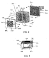
- FIG. 2 is a perspective view of one embodiment of the waveguide adapter 100 of the present invention shown with a conventional rectangular waveguide 300 at one end and a grid array assembly 200, comprising an active quasi-optic grid array 202 associated with a dielectric layer 208, at the.other end, both in position to be assembled to the adapter.
- FIG. 3 is perspective cutaway illustration of a typical adapter 100 of the present invention, such as the one shown in FIG. 2.
- the first end 110 of the adapter of the present invention defines a first aperture 120 that is designed to match, or mate with, an aperture 320 at an end 310 of a typical rectangular waveguide 300 that propagates signals in the TE single mode.
- Steps 102, 104, 106 and 108 in both the horizontal and vertical planes expand the internal size of the guiding structure 100 from the standard fundamental single-mode waveguide size at the first aperture 120 to the oversized guide aperture defined by the second end 130 of the adapter that is equal to or larger than the size of the active array 202.
- These steps define the conducting walls 122, 124, 126 within which the EM signal propagates.
- steps 102 and 104 enlarge the guide (as viewed from the waveguide) in the direction parallel to the electric field in the standard guide and are thus referred to as "E-plane” steps.
- Steps 106 and 108 are perpendicular to both the electric field and the longitudinal direction of propagation, and are thus referred to as "H-plane" steps.
- Each step creates a spatial discontinuity within the cavity, which is a relatively abrupt change in the cross-section of the cavity and as defined above.
- the step need not be machined to create a "sharp" corner.
- the step should create change in cross-section occur over less than a quarter of a wavelength of radiation and may differ depending on the specific application.
- the number, placement and size of the steps control the amplitude and phase distribution at the plane of the grid array, or second end 130, and can be adjusted as desired.
- one or more sheets of dielectric 208 may be used to provide impedance matching between the modes excited in the oversized guide and the active array.
- one surface of a sheet of dielectric supports the grid array 202 and the entire grid array-dielectric assembly can be assembled into and contained by the second end 130 of the adapter 100.
- the number of propagating modes within the dielectrically loaded portion of the guide is larger than in the air-filled portion.
- the steps excite higher-order modes within the guiding structure of the adapter 100. These modes may be either propagating or evanescent.
- the magnitude and phase of these excitations with respect to the fundamental mode are determined by the lateral size and longitudinal position of the steps. By controlling the magnitude and phase of these excitations, a conversion between the fundamental standard waveguide mode at aperture 120 and an approximation to a desired field distribution (e.g ., uniform amplitude and phase) at the plane of the active array 130 is achieved.
- the number of higher order modes that may be independently controlled is determined by the number of steps used to expand from the standard guide to the oversized guide. A larger number of smaller steps can allow greater flexibility in tailoring the shape of the field distribution at the plane of the active array.
- the distances, w, x, y and z from the edges 222, 224, 226, 228 of the active array, to the edges of the second end 130 of the adapter 100, in this case, the walls 126, 127, 128 and 129, is also important in determining the field distribution, and provides an additional design parameter for improving the distribution.
- a first approximation to the step design can be made using a spatial Fourier series expansion in the modes available to propagate within the oversized guide.
- the magnitude and phase of the expansion coefficients depend on the size and longitudinal placement of the steps.
- FIG. 2 is a particular illustration of an adapter configured as an input feed to a grid amplifier. That is, this adapter feeds a signal from a waveguide to a grid array such as a grid amplifier and with the amplifier providing a free space output.
- the adapter of the present invention operated equally in the reverse mode. That is, the adapter of the present invention may operate as an efficient output waveguide collector or "mode contractor."
- the grid array radiates in free space a multiple mode output power signal into the oversized adapter 100, which collects this free space signal and reduces the signal down to a signal mode TEM signal, via the adapter's steps that contract its internal cavity, for input to a standard TEM waveguide.
- the internal wave-confining structure is typically electrically conducting walls but may alternatively be non-conducting.
Landscapes
- Power Engineering (AREA)
- Engineering & Computer Science (AREA)
- Optical Integrated Circuits (AREA)
- Amplifiers (AREA)
- Optical Modulation, Optical Deflection, Nonlinear Optics, Optical Demodulation, Optical Logic Elements (AREA)
- Microwave Amplifiers (AREA)
- Waveguides (AREA)
- Optical Couplings Of Light Guides (AREA)
- Semiconductor Lasers (AREA)
- Electrical Discharge Machining, Electrochemical Machining, And Combined Machining (AREA)
- Hybrid Cells (AREA)
- Optical Radar Systems And Details Thereof (AREA)
- Apparatus For Radiation Diagnosis (AREA)
- Reinforced Plastic Materials (AREA)
- Ropes Or Cables (AREA)
Abstract
Description
- This invention relates to quasi-optic grid arrays, such as periodic grid arrays, and in particular to techniques for adapting a waveguide to a quasi-optic grid array.
- Broadband communications, radar and other imaging systems require the transmission of radio frequency ("RF") signals in the microwave and millimeter wave bands. In order to efficiently achieve the levels of output transmission power needed for many applications at these high frequencies, a technique called "power combining" has been employed, whereby the output power of individual components are coupled, or combined, thereby creating a single power output that is greater than an individual component can supply. Conventionally, power combining has used resonant waveguide cavities or transmission-line feed networks. These approaches, however, have a number of shortcomings that become especially apparent at higher frequencies. First, conductor losses in the waveguide walls or transmission lines tend to increase with frequency, eventually limiting the combining efficiency. Second, these resonant waveguide cavities or transmission-line combiners.become increasingly difficult to machine as the wavelength gets smaller. Third, in waveguide systems, each device often must be inserted and tuned manually. This is labor-intensive and only practical for a relatively small number of devices.
- Several years ago, spatial power combining using "quasi-optics" was proposed as a potential solution to these problems. The theory was that an array of microwave or millimeter-wave solid state sources placed in a resonator could synchronize to the same frequency and phase, and their outputs would combine in free space, minimizing conductor losses. Furthermore, a planar array could be fabricated monolithically and at shorter wavelengths, thereby enabling potentially thousands of devices to be incorporated on a single wafer.
- Since then, numerous quasi-optical devices have been developed, including detectors, multipliers, mixers, and phase shifters. These passive devices continue to be the subject of ongoing research. Over the past few years, however, active quasi-optical devices, namely oscillators and amplifiers, have evolved. One benefit of spatial power combining (over other methods) using quasi-optics is that the output power scales linearly with chip area. Thus, the field of active quasi-optics has attracted considerable attention in a short time, and the growth of the field has been explosive.
- It is believed that the first quasi-optical grid array amplifier was a grid developed by M. Kim et al. at the California Institute of Technology. This grid used 25 MESFET differential pairs, demonstrating a gain of 11 dB at 3 GHz. As shown in FIG. 1, a typical grid amplifier 10 is an array of closely-spaced differential pairs of
transistors 14 on anactive grid 12 sandwiched between an input and output polarizer, 18, 24. Aninput signal 16 passes through the horizontally polarizedinput polarizer 18 and creates an input beam incident from the left that excites rf currents on the horizontally polarizedinput antennas 20 of thegrid 12. These currents drive the inputs of thetransistor pair 14 in the differential mode. The output currents are redirected along the grid's vertically polarizedantennas 22, producing a vertically polarizedoutput beam 30 via anoutput polarizer 24 to the right. - The cross-polarized input and output affords two important advantages. First, it provides good input-output isolation, reducing the potential for spurious feedback oscillations. Second, the amplifier's input and output circuits can be independently tuned using metal-strip polarizers, which also confine the beam to the forward direction. Numerous grid amplifiers have since been developed and have proven thus far to have great promise for both military and commercial RF applications and particularly for high frequency, broadband systems that require significant output power levels (e.g. > 5 watts) in a small, preferably monolithic, package. Moreover, a resonator can be used to provide feedback to couple the active devices to form a high power oscillator.
- Grids amplifiers can be characterized as quasi-plane wave input, quasi-plane wave output (free space) devices. Grid oscillators are essentially quasi-plane wave output devices. However, most microwave and millimeter wave systems transport signals through electrical waveguides, which are devices that have internal wave-guiding cavities bounded by wave-confining, and typically metal, walls. Consequently, an interface between the two environments is needed in most cases. This interface is needed whether the electric field signal is being output from a waveguide for effective application to the grid array; or the free space output signal of a grid array is to be collected into a waveguide.
- Providing such an interface is not a trivial matter for several reasons. First, microwave and millimeter wave waveguides conventionally transmit signals in the single transverse electric (TE) mode, also known as the fundamental, or TE10, mode, and block the higher-order mode components of the signal. These conventional waveguides have a standard, constant size and rectangular shape. However, the input plane area of any typical grid array upon which the input signal is incident may be much larger than the area of the standard rectangular waveguide aperture. Furthermore, as noted, grid array assemblies comprising N by N unit cells and bounded by a dielectric (see FIG. 2) will vary in size depending number of cells in the grid and the dielectric size. Thus, a standard waveguide cannot directly mate with a grid array structure.
- Moreover, the standard single mode rectangular waveguide operating in TE10 mode provides an electric field distribution that varies sinusoidally in amplitude across it aperture. However, efficient operation of grid amplifiers requires an excitation beam that has a relatively uniform phase and magnitude distribution across the amplifier's area.
- Several groups have attempted to design waveguides that interface with quasi-optic active devices, but have had only limited success. For example, Yang, et al. recently published an article titled "A Novel TEM Waveguide using Unipolar Compact Photonic-Bandgap ", IEEE Trans. On Microwave Theory and Tech., Vol. 48, No. 2, pp. 2092-2098, Nov., 1999. Further, Ali, et al. published an article titled, "Analysis and Measurement of Hard-Horn Feeds for the Excitation of Quasi-Optic Amplifiers," IEEE Trans. On Microwave Theory and Tech., Vol. 47, No. 4, pp. 479-487. April 1999. Unfortunately, these proposed techniques do not adequately resolve the aforementioned problems. For example, the photonic bandgap structures described by Yang et al. are very difficult and costly to manufacture, making this technique less than desirable. Moreover, the "hard-horn" approach of Ali et al. creates a rather large and bulky structure that is impractical for most commercial applications.
- US 4,757,326 discloses a box horn antenna with linearized aperture distribution into polarisations. A horn comprising a number of vanes is used to produce a step in the H plane, converting some of the incident TE1,0 mode energy in to TE3.0 mode energy. The horn is used to create a field antenna, and relies upon the vanes preventing an abrupt step in the E plane.
- US 2,617,937 also discloses a flared horn wave guide antenna, which converts TE1,0 mode energy into TE3,0 energy by using a horn which is flared either in the E plane or H plane.
- Ali et al (IEEE US, 3,1998,pp 1469-1472) disclose a double layer amplifier array (a quasi-optic grid ray) placed between a feeding hard horn antenna and a collecting hard horn antenna.
- Thus, there is a definite need for a simple and cost effective interface, or adapter, that efficiently couples a waveguide that propagates signals in the fundamental mode to a grid array structure with a desired field distribution.
- The invention is defined by the independent claims to which reference should be made.
- The present invention, which addresses these needs, resides in an adapter for coupling a quasi-optic grid array to a rectangular waveguide according to independent claim 1.
- The invention also resides in a corresponding method as set out in independent claim 9.
- Specific embodiments are defined in the dependent claims.
-
- FIG. 1 is an exploded view of a conventional quasi-optic grid array with one of the differential pair unit cells in the array magnifield;
- FIG. 2 is a perspective view of a waveguide adapter of the present invention shown with a rectangular waveguide in position to be assembled to it at one end and an active quasi-optic grid array assembly in position to be assembled into the adapter at one end; and
- FIG. 3 is a perspective cutaway illustration of the adapter of the present invention shown with one step provided in the E-plane and one step in the H-plane.
- The invention disclosed here is an adapter or transition between the waveguide environment and the quasi-plane wave (quasi-TEM mode) environment in which the grid array components operate. Efficient operation of grid amplifiers requires an excitation beam that has a uniform phase and magnitude over the amplifier's area. Efficient operation also requires that a the output field distribution of the grid array (typically essentially uniform in amplitude and phase, although alternative distributions are possible) be strongly coupled to the fundamental mode of a waveguide structure, if the output of the grid array is to be recaptured into a guided wave environment (rather than radiated into free space).
- As noted, single-mode rectangular waveguide operating in TE10 mode gives an electric field distribution that varies sinusoidally in amplitude across its aperture. The waveguide adapter disclosed herein couples this fundamental TE10 mode in a standard waveguide to higher-order modes in an oversized guide with desired amplitude and phase relationships, so as to provide efficient excitation of the grid array when used as an input feed. In reverse operation, the adapter serves as an efficient collector of output power when used as an output waveguide transition.
- FIG. 2 is a perspective view of one embodiment of the
waveguide adapter 100 of the present invention shown with a conventionalrectangular waveguide 300 at one end and agrid array assembly 200, comprising an activequasi-optic grid array 202 associated with adielectric layer 208, at the.other end, both in position to be assembled to the adapter. FIG. 3 is perspective cutaway illustration of atypical adapter 100 of the present invention, such as the one shown in FIG. 2. Thefirst end 110 of the adapter of the present invention defines afirst aperture 120 that is designed to match, or mate with, anaperture 320 at anend 310 of a typicalrectangular waveguide 300 that propagates signals in the TE single mode.Steps structure 100 from the standard fundamental single-mode waveguide size at thefirst aperture 120 to the oversized guide aperture defined by thesecond end 130 of the adapter that is equal to or larger than the size of theactive array 202. These steps define the conductingwalls Steps second end 130, and can be adjusted as desired. - In addition to the confining structure, or the walls, of the adapter, one or more sheets of
dielectric 208 may be used to provide impedance matching between the modes excited in the oversized guide and the active array. In the embodiment shown in FIG. 2, one surface of a sheet of dielectric supports thegrid array 202 and the entire grid array-dielectric assembly can be assembled into and contained by thesecond end 130 of theadapter 100. Typically, the number of propagating modes within the dielectrically loaded portion of the guide is larger than in the air-filled portion. - The steps excite higher-order modes within the guiding structure of the
adapter 100. These modes may be either propagating or evanescent. The magnitude and phase of these excitations with respect to the fundamental mode are determined by the lateral size and longitudinal position of the steps. By controlling the magnitude and phase of these excitations, a conversion between the fundamental standard waveguide mode ataperture 120 and an approximation to a desired field distribution (e.g., uniform amplitude and phase) at the plane of theactive array 130 is achieved. The number of higher order modes that may be independently controlled is determined by the number of steps used to expand from the standard guide to the oversized guide. A larger number of smaller steps can allow greater flexibility in tailoring the shape of the field distribution at the plane of the active array. - Moreover, when assembled, the distances, w, x, y and z from the
edges second end 130 of theadapter 100, in this case, thewalls - A first approximation to the step design can be made using a spatial Fourier series expansion in the modes available to propagate within the oversized guide. The magnitude and phase of the expansion coefficients depend on the size and longitudinal placement of the steps.
- As noted, FIG. 2 is a particular illustration of an adapter configured as an input feed to a grid amplifier. That is, this adapter feeds a signal from a waveguide to a grid array such as a grid amplifier and with the amplifier providing a free space output. However, it should be understood that the present invention operated equally in the reverse mode. That is, the adapter of the present invention may operate as an efficient output waveguide collector or "mode contractor." In this embodiment, the grid array radiates in free space a multiple mode output power signal into the
oversized adapter 100, which collects this free space signal and reduces the signal down to a signal mode TEM signal, via the adapter's steps that contract its internal cavity, for input to a standard TEM waveguide. - It should be understood that the internal wave-confining structure is typically electrically conducting walls but may alternatively be non-conducting.
- Having thus described exemplary embodiments of the invention, it will be apparent that further alterations, modifications, and improvements will also occur to those skilled in the art.
Claims (15)
- An adapter for coupling a quasi-optic grid (202) array to a rectangular waveguide (300) having an Internal cavity defined by a wave-confining device and that guides a wave propagating in a longitudinal direction, the adapter (100) translating between the fundamental mode of the waveguide and a desired electromagnetic field distribution at the plane of the array (202), comprising:(a) a first end (110) that is adapted to substantially mate with the rectangular waveguide (300) and that defines a first rectangular aperture (120) that substantially matches the size of the waveguide cavity to receive and direct an electromagnetic wave polarized in a single direction of polarization; and;(b) a second end (130) defining a second rectangular aperture that is larger than the first rectangular aperture (120) electromagnetically coupled to the first rectangular aperture; and(c) means disposed between the first end (110) and second end (130) defining a wave-guiding cavity for guiding a wave propagating along the longitudinal direction of signal propagation, the means including a first step (102) configured within the wave-guiding cavity at a predetermined distance from the first aperture (120) creating a spatial discontinuity along the single direction of polarization of the electromagnetic wave received at the first and (110); said step (102) being of a predetermined size and distance from the plane of the quasi-optic grid array (202) to create a desired electric and magnetic field distribution at the quasi-optic grid array (202); characterized by said means further including a second step (106) within the wave-guiding cavity that is positioned between the first step (102) and the second end (130) creating a second spatial discontinuity along a direction perpendicular to both the single direction of polarization of the electromagnetic wave and the longitudinal direction of wave propagation.
- The adapter (100) of claim 1, further including at least one additional step (104) within the wave-guiding cavity that creates a spatial discontinuity in a direction parallel to the single direction of polarization of the electromagnetic wave received at the first end (110) or at least one additional step (108) within the wave-guiding cavity that creates a spatial discontinuity in a direction perpendicular to both the single direction of polarization of the electromagnetic wave received at the first end (110) and the direction of wave propagation all steps being configured to excite higher order modes within the adapter (100) and to shape the field distribution of the signal at the second aperture.
- The adapter (100) of claim 1 or 2, wherein the second end (130) of the adapter is arranged to contain the grid array (202).
- The adapter (100) of daim 1 or 2, wherein the second end (130) of the adapter (100) contains the grid array (202) that is bounded by a dielectric sheet (208).
- The adapter (100) of claim 1, wherein the second end (130) of the adapter (100) contains a grid amplifier that is bounded by a dielectric sheet (208).
- The adapter (100) of claim 4, wherein the dielectric is a heat spreader.
- The adapter (100) of claim 4, wherein the second aperture is sized such that the edges of the grid array (202) are spaced apart from the wave-confining structure at the second end (130) a predetermined distance in order to shape the field distribution incident at the second aperture.
- The adapter (100) of claim 1 or 2, further including additional steps within the cavity.
- A method of translating an electromagnetic signal between the fundamental mode of a rectangular waveguide (300) at a first end (110) of a waveguide adapter (100) having an internal cavity defined by a wave-confining device that guides a wave propagating in a longitudinal direction, and a field distribution that is desirable for a quasi-optic grid array (202) at a second end (130) of the waveguide adapter (100), the first end (110) being adapted to substantially mate with the rectangular waveguide (300) and defining first rectangular aperture (120) that substantially matches the size of the waveguide cavity to receive and direct an electromagnetic wave polarized in a single direction of polarization,
the second end (130) defining a second rectangular aperture that is larger than the first rectangular aperture (120) electromagnetically coupled to the first rectangular aperture, providing means between the first end (110) and second end (130) defining a wave-guiding cavity for guiding a wave propagating along the longitudinal direction of signal propagation, the means including a first step (102) configured within the wave-guiding cavity at a predetermined distance from the first aperture (120) creating a spatial discontinuity along the single direction of polarization of the electromagnetic wave received at the first end (110); said step (102) being of a predetermined size and distance from the plane of the quasi-optic grid array (202) to create a desired electric and magnetic field distribution at the quasi-optic grid array (202); characterized by said means further including a second step (106) within the wave-guiding cavity that is positioned between the first step (102) and the second end (130) creating a second spatial discontinuity, along a direction perpendicular to both the single direction of polarization of the electromagnetic wave and the longitudinal direction of wave propagation. - The method of claim 9, further including providing the grid array (202), with a dielectric bounding the array, at the second end (130) of the adapter (100) and adjusting the normal distance between the edge of the grid array (202) and the adapter (100) at the second end (130) to further determine the field distribution on the grid array (202).
- Use of the adapter (100) of claim 7 as an input feed device.
- Use of the adapter (100) of claim 7 as an EM wave collector device.
- A system comprising the adapter (100) of claim 1, and further comprising:a quasi-optic grid array (202) coupled to said second end (130);a dielectric layer (208) larger than said grid array (202) and positioned between said grid array (202) and said second end (130) to match an impedance between an electromagnetic field at said grid array (202) and an electromagnetic field at said second end (130); anda waveguide (300) having a waveguide end opening that substantially conformingly connects to said first end (110).
- The system as in claim 13, wherein the spacing from each side of said grid array (202) to an adjacent edge of said second end (120) of said waveguide adapter (100) is determined by said desired field distribution.
- The system as in claim 14, wherein each step structure (102,106) is configured to produce a change in a cross section of said wave-guiding cavity over a distance of less than one quarter of one wavelength of the electromagnetic wave in the direction of propagation of the wave.
Priority Applications (1)
| Application Number | Priority Date | Filing Date | Title |
|---|---|---|---|
| EP06021741A EP1770821A1 (en) | 2000-06-13 | 2001-06-05 | Mode translating waveguide adapter for a quasi-optic grid array |
Applications Claiming Priority (3)
| Application Number | Priority Date | Filing Date | Title |
|---|---|---|---|
| US21125200P | 2000-06-13 | 2000-06-13 | |
| US211252P | 2000-06-13 | ||
| PCT/US2001/018473 WO2001097322A1 (en) | 2000-06-13 | 2001-06-05 | Mode translating waveguide adapter for a quasi-optic grid array |
Related Child Applications (1)
| Application Number | Title | Priority Date | Filing Date |
|---|---|---|---|
| EP06021741A Division EP1770821A1 (en) | 2000-06-13 | 2001-06-05 | Mode translating waveguide adapter for a quasi-optic grid array |
Publications (2)
| Publication Number | Publication Date |
|---|---|
| EP1295356A1 EP1295356A1 (en) | 2003-03-26 |
| EP1295356B1 true EP1295356B1 (en) | 2006-10-18 |
Family
ID=22786140
Family Applications (2)
| Application Number | Title | Priority Date | Filing Date |
|---|---|---|---|
| EP01944340A Expired - Lifetime EP1295356B1 (en) | 2000-06-13 | 2001-06-05 | Mode translating waveguide adapter for a quasi-optic grid array |
| EP01946157A Expired - Lifetime EP1293011B1 (en) | 2000-06-13 | 2001-06-05 | Techniques for enhancing gain in a quasi-optic grid array |
Family Applications After (1)
| Application Number | Title | Priority Date | Filing Date |
|---|---|---|---|
| EP01946157A Expired - Lifetime EP1293011B1 (en) | 2000-06-13 | 2001-06-05 | Techniques for enhancing gain in a quasi-optic grid array |
Country Status (11)
| Country | Link |
|---|---|
| US (4) | US6559724B2 (en) |
| EP (2) | EP1295356B1 (en) |
| JP (1) | JP3831339B2 (en) |
| AT (2) | ATE343229T1 (en) |
| AU (3) | AU2001268240A1 (en) |
| DE (2) | DE60123953T2 (en) |
| ES (2) | ES2273850T3 (en) |
| IL (2) | IL153112A0 (en) |
| MX (1) | MXPA02012381A (en) |
| TW (3) | TW495820B (en) |
| WO (3) | WO2001097328A1 (en) |
Families Citing this family (37)
| Publication number | Priority date | Publication date | Assignee | Title |
|---|---|---|---|---|
| US6876272B2 (en) * | 2001-10-23 | 2005-04-05 | Wavestream Wireless Technologies | Reflection-mode, quasi-optical grid array wave-guiding system |
| GB0220434D0 (en) * | 2002-09-03 | 2004-03-17 | Qinetiq Ltd | Detection device |
| US7110165B2 (en) * | 2002-10-29 | 2006-09-19 | Wavestream Wireless Technologies | Power management for spatial power combiners |
| WO2005022778A1 (en) * | 2003-09-03 | 2005-03-10 | Koninkijke Philips Electronics N.V. | Diversity receiver |
| US7327803B2 (en) | 2004-10-22 | 2008-02-05 | Parkervision, Inc. | Systems and methods for vector power amplification |
| US7355470B2 (en) | 2006-04-24 | 2008-04-08 | Parkervision, Inc. | Systems and methods of RF power transmission, modulation, and amplification, including embodiments for amplifier class transitioning |
| US7205836B2 (en) * | 2005-05-03 | 2007-04-17 | M/A-Com, Inc. | SiGe differential cascode amplifier with miller effect resonator |
| US7784390B1 (en) | 2005-08-18 | 2010-08-31 | Raytheon Company | Solid-state non-lethal directed energy weapon |
| US7443573B2 (en) * | 2005-09-20 | 2008-10-28 | Raytheon Company | Spatially-fed high-power amplifier with shaped reflectors |
| US7911272B2 (en) | 2007-06-19 | 2011-03-22 | Parkervision, Inc. | Systems and methods of RF power transmission, modulation, and amplification, including blended control embodiments |
| US8013675B2 (en) | 2007-06-19 | 2011-09-06 | Parkervision, Inc. | Combiner-less multiple input single output (MISO) amplification with blended control |
| US8334722B2 (en) | 2007-06-28 | 2012-12-18 | Parkervision, Inc. | Systems and methods of RF power transmission, modulation and amplification |
| US7378914B2 (en) * | 2006-01-31 | 2008-05-27 | Raytheon Company | Solid-state high-power oscillators |
| US7403076B1 (en) | 2006-02-03 | 2008-07-22 | Hrl Laboratories, Llc | High frequency quasi optical power source capable of solid state implementation |
| US8031804B2 (en) | 2006-04-24 | 2011-10-04 | Parkervision, Inc. | Systems and methods of RF tower transmission, modulation, and amplification, including embodiments for compensating for waveform distortion |
| US7937106B2 (en) * | 2006-04-24 | 2011-05-03 | ParkerVision, Inc, | Systems and methods of RF power transmission, modulation, and amplification, including architectural embodiments of same |
| US7504999B2 (en) * | 2006-08-22 | 2009-03-17 | Raytheon Company | Amplified patch antenna reflect array |
| US8315336B2 (en) * | 2007-05-18 | 2012-11-20 | Parkervision, Inc. | Systems and methods of RF power transmission, modulation, and amplification, including a switching stage embodiment |
| US7620129B2 (en) | 2007-01-16 | 2009-11-17 | Parkervision, Inc. | RF power transmission, modulation, and amplification, including embodiments for generating vector modulation control signals |
| CA2678741A1 (en) * | 2007-02-20 | 2008-08-28 | Wavestream Corporation | Energy focusing system for active denial apparatus |
| US8182103B1 (en) | 2007-08-20 | 2012-05-22 | Raytheon Company | Modular MMW power source |
| US8565861B2 (en) * | 2008-05-02 | 2013-10-22 | Olympus Corporation | Optical inspection device, electromagnetic wave detection method, electromagnetic wave detection device, organism observation method, microscope, endoscope, and optical tomographic image generation device |
| WO2009145887A1 (en) | 2008-05-27 | 2009-12-03 | Parkervision, Inc. | Systems and methods of rf power transmission, modulation, and amplification |
| US8107894B2 (en) | 2008-08-12 | 2012-01-31 | Raytheon Company | Modular solid-state millimeter wave (MMW) RF power source |
| US8248320B2 (en) * | 2008-09-24 | 2012-08-21 | Raytheon Company | Lens array module |
| US9375169B2 (en) | 2009-01-30 | 2016-06-28 | Sanofi-Aventis Deutschland Gmbh | Cam drive for managing disposable penetrating member actions with a single motor and motor and control system |
| GB2467763B (en) * | 2009-02-13 | 2013-02-20 | Univ Kent Canterbury | Tuneable surface |
| US8058935B2 (en) | 2010-02-05 | 2011-11-15 | The Boeing Company | Scalable millimeter wave power source |
| KR20140026458A (en) | 2011-04-08 | 2014-03-05 | 파커비전, 인크. | Systems and methods of rf power transmission, modulation, and amplification |
| JP6174574B2 (en) | 2011-06-02 | 2017-08-02 | パーカーヴィジョン インコーポレイテッド | Antenna control |
| US8552813B2 (en) | 2011-11-23 | 2013-10-08 | Raytheon Company | High frequency, high bandwidth, low loss microstrip to waveguide transition |
| EP3047348B1 (en) | 2013-09-17 | 2025-03-19 | Parkervision, Inc. | Method for rendering an information bearing function of time |
| EP2943992A1 (en) * | 2013-11-19 | 2015-11-18 | CommScope Technologies LLC | Modular feed assembly |
| JP6504995B2 (en) * | 2015-10-30 | 2019-04-24 | アンリツ株式会社 | Feedback amplification circuit and frequency characteristic control method thereof |
| CN109286080B (en) * | 2018-10-23 | 2021-01-12 | 北京无线电测量研究所 | Polarization device |
| US10749256B1 (en) * | 2019-01-30 | 2020-08-18 | Raytheon Company | Waveguide adapter for slot antennas |
| CN114284654B (en) * | 2021-11-23 | 2023-05-12 | 电子科技大学 | Circular waveguide TM loaded by special-shaped grating 01 -TE 01 Mode converter |
Family Cites Families (16)
| Publication number | Priority date | Publication date | Assignee | Title |
|---|---|---|---|---|
| US2617937A (en) * | 1945-09-14 | 1952-11-11 | Lester C Van Atta | Flared horn wave guide antenna |
| US2957143A (en) * | 1959-09-11 | 1960-10-18 | Arizona Res Foundation | Wideband transistor amplifier |
| DE3873384T2 (en) * | 1987-03-20 | 1992-12-24 | Toshiba Kawasaki Kk | TAX-GENERATING DIFFERENTIAL CIRCUIT. |
| US4757326A (en) * | 1987-03-27 | 1988-07-12 | General Electric Company | Box horn antenna with linearized aperture distribution in two polarizations |
| US5214394A (en) * | 1991-04-15 | 1993-05-25 | Rockwell International Corporation | High efficiency bi-directional spatial power combiner amplifier |
| DE69215492T2 (en) * | 1991-12-23 | 1997-05-22 | Philips Electronics Nv | Semiconductor arrangement with two-stage differential amplifier |
| US5317173A (en) * | 1993-05-13 | 1994-05-31 | Rockwell International Corporation | HBT differential pair chip for quasi-optic amplifiers |
| US5392152A (en) * | 1993-10-13 | 1995-02-21 | Rockwell International Corporation | Quasi-optic amplifier with slot and patch antennas |
| EP0673111A1 (en) * | 1994-03-17 | 1995-09-20 | ALCATEL BELL Naamloze Vennootschap | Differential pair arrangement |
| US5481223A (en) * | 1994-09-13 | 1996-01-02 | Rockwell International Corporation | Bi-directional spatial power combiner grid amplifier |
| US5450041A (en) * | 1994-09-19 | 1995-09-12 | The United States Of America As Represented By The Secretary Of The Army | Quasi-optical oscillator using ring-resonator feedback |
| US5900779A (en) * | 1996-06-13 | 1999-05-04 | Vtc, Inc. | Differential transimpedance amplifier |
| FI107657B (en) * | 1998-03-11 | 2001-09-14 | Nokia Mobile Phones Ltd | Coupling to control the impedance of a differential active component |
| US5900965A (en) * | 1998-05-06 | 1999-05-04 | The United States Of America As Represented By The Secretary Of The Army | Wideband quasi-optical millimeter-wave resonator |
| US6069523A (en) * | 1998-06-04 | 2000-05-30 | Nortel Networks Corporation | Differential data driver |
| JP4206589B2 (en) * | 1999-12-02 | 2009-01-14 | 富士通株式会社 | Distributed amplifier |
-
2001
- 2001-06-05 ES ES01944340T patent/ES2273850T3/en not_active Expired - Lifetime
- 2001-06-05 WO PCT/US2001/018478 patent/WO2001097328A1/en not_active Ceased
- 2001-06-05 AU AU2001268240A patent/AU2001268240A1/en not_active Abandoned
- 2001-06-05 US US09/876,210 patent/US6559724B2/en not_active Expired - Lifetime
- 2001-06-05 US US09/876,211 patent/US6538793B2/en not_active Expired - Lifetime
- 2001-06-05 US US09/876,212 patent/US6542662B2/en not_active Expired - Lifetime
- 2001-06-05 DE DE60123953T patent/DE60123953T2/en not_active Expired - Lifetime
- 2001-06-05 JP JP2002511421A patent/JP3831339B2/en not_active Expired - Lifetime
- 2001-06-05 WO PCT/US2001/018477 patent/WO2001097259A2/en not_active Ceased
- 2001-06-05 EP EP01944340A patent/EP1295356B1/en not_active Expired - Lifetime
- 2001-06-05 IL IL15311201A patent/IL153112A0/en active IP Right Grant
- 2001-06-05 AT AT01946157T patent/ATE343229T1/en not_active IP Right Cessation
- 2001-06-05 AT AT01944340T patent/ATE343226T1/en not_active IP Right Cessation
- 2001-06-05 AU AU2001268239A patent/AU2001268239A1/en not_active Abandoned
- 2001-06-05 MX MXPA02012381A patent/MXPA02012381A/en active IP Right Grant
- 2001-06-05 AU AU2001266763A patent/AU2001266763A1/en not_active Abandoned
- 2001-06-05 US US09/876,835 patent/US6583672B2/en not_active Expired - Lifetime
- 2001-06-05 EP EP01946157A patent/EP1293011B1/en not_active Expired - Lifetime
- 2001-06-05 ES ES01946157T patent/ES2273855T3/en not_active Expired - Lifetime
- 2001-06-05 WO PCT/US2001/018473 patent/WO2001097322A1/en not_active Ceased
- 2001-06-05 DE DE60123955T patent/DE60123955T2/en not_active Expired - Lifetime
- 2001-06-13 TW TW090114333A patent/TW495820B/en not_active IP Right Cessation
- 2001-06-13 TW TW090114334A patent/TW508880B/en not_active IP Right Cessation
- 2001-06-13 TW TW090114335A patent/TW508881B/en not_active IP Right Cessation
-
2002
- 2002-11-26 IL IL153112A patent/IL153112A/en unknown
Also Published As
| Publication number | Publication date |
|---|---|
| ES2273850T3 (en) | 2007-05-16 |
| US20020024719A1 (en) | 2002-02-28 |
| US20020024387A1 (en) | 2002-02-28 |
| US6583672B2 (en) | 2003-06-24 |
| IL153112A0 (en) | 2003-06-24 |
| DE60123955D1 (en) | 2006-11-30 |
| TW495820B (en) | 2002-07-21 |
| DE60123955T2 (en) | 2007-06-14 |
| MXPA02012381A (en) | 2004-01-26 |
| EP1293011B1 (en) | 2006-10-18 |
| ATE343226T1 (en) | 2006-11-15 |
| ATE343229T1 (en) | 2006-11-15 |
| AU2001266763A1 (en) | 2001-12-24 |
| AU2001268240A1 (en) | 2001-12-24 |
| US6542662B2 (en) | 2003-04-01 |
| JP2004503970A (en) | 2004-02-05 |
| TW508881B (en) | 2002-11-01 |
| ES2273855T3 (en) | 2007-05-16 |
| DE60123953D1 (en) | 2006-11-30 |
| AU2001268239A1 (en) | 2001-12-24 |
| WO2001097328A1 (en) | 2001-12-20 |
| US20020018282A1 (en) | 2002-02-14 |
| WO2001097259A2 (en) | 2001-12-20 |
| JP3831339B2 (en) | 2006-10-11 |
| IL153112A (en) | 2006-06-11 |
| US6559724B2 (en) | 2003-05-06 |
| WO2001097322A1 (en) | 2001-12-20 |
| US20020021865A1 (en) | 2002-02-21 |
| EP1293011A1 (en) | 2003-03-19 |
| EP1295356A1 (en) | 2003-03-26 |
| US6538793B2 (en) | 2003-03-25 |
| TW508880B (en) | 2002-11-01 |
| DE60123953T2 (en) | 2007-07-05 |
Similar Documents
| Publication | Publication Date | Title |
|---|---|---|
| US6542662B2 (en) | Mode translating waveguide adapter for a quasi-optic grid array | |
| Perkons et al. | TM surface-wave power combining by a planar active-lens amplifier | |
| EP0203777B1 (en) | Space amplifier | |
| Ghanadi | A new compact broadband radial power combiner | |
| Kanamaluru et al. | Analysis and design of aperture-coupled microstrip patch antennas and arrays fed by dielectric image line | |
| Baghel et al. | Slot antenna excited by novel substrate integrated coaxial line cavity for millimetre wave application | |
| Weikle et al. | Transistor oscillator and amplifier grids | |
| US7242518B1 (en) | Standing wave amplifiers and oscillators | |
| Perkons et al. | A 10-element active lens amplifier on a dielectric slab | |
| Galli et al. | Leaky‐Wave Antennas | |
| US6876272B2 (en) | Reflection-mode, quasi-optical grid array wave-guiding system | |
| Schulwitz et al. | Millimeter-wave dual polarized L-shaped horn antenna for wide-angle phased arrays | |
| Ortiz | High power spatial combiners: Tile and tray approaches | |
| Zhou et al. | Technology assessment of aperture coupled slot antenna array in groove gapwaveguide for 5G millimeter wave applications | |
| EP1770821A1 (en) | Mode translating waveguide adapter for a quasi-optic grid array | |
| Hicks et al. | Spatial power combining for two-dimensional structures | |
| Yin et al. | Characterization and design of millimeter-wave full-band waveguide-based spatial power divider/combiner | |
| Belaid et al. | Integrated active antenna array using unidirectional dielectric radiators | |
| Cheung et al. | A waveguide mode-converter feed for a 5-W, 34-GHz grid amplifier | |
| Liu et al. | Design and Cold Test Study of W-Band Suspended Multi-channel Array Integrated Microstrip Meander Line Traveling-Wave Tubes | |
| Chen et al. | Theoretical designs and experiments on dual-band input coupler for gyrotron traveling wave tube | |
| Zhang et al. | Dielectric resonator probe arrays with sectoral hard horn for wideband spatial power combiners/dividers | |
| Chen et al. | A frequency agile beam steerable tapered dielectric image-line antenna array with novel feeding structure | |
| Kawasaki et al. | 2* 2 quasi-optical power combiner array at 20 GHz | |
| Suresh et al. | Review on SIW Antennas for mm-wave band of 5G Communications |
Legal Events
| Date | Code | Title | Description |
|---|---|---|---|
| PUAI | Public reference made under article 153(3) epc to a published international application that has entered the european phase |
Free format text: ORIGINAL CODE: 0009012 |
|
| 17P | Request for examination filed |
Effective date: 20021230 |
|
| AK | Designated contracting states |
Designated state(s): AT BE CH CY DE DK ES FI FR GB GR IE IT LI LU MC NL PT SE TR Kind code of ref document: A1 Designated state(s): AT BE CH CY DE DK ES FI FR GB GR IE IT LI LU MC NL PT SE TR |
|
| AX | Request for extension of the european patent |
Extension state: AL LT LV MK RO SI |
|
| 17Q | First examination report despatched |
Effective date: 20030617 |
|
| GRAP | Despatch of communication of intention to grant a patent |
Free format text: ORIGINAL CODE: EPIDOSNIGR1 |
|
| GRAS | Grant fee paid |
Free format text: ORIGINAL CODE: EPIDOSNIGR3 |
|
| GRAA | (expected) grant |
Free format text: ORIGINAL CODE: 0009210 |
|
| AK | Designated contracting states |
Kind code of ref document: B1 Designated state(s): AT BE CH CY DE DK ES FI FR GB GR IE IT LI LU MC NL PT SE TR |
|
| PG25 | Lapsed in a contracting state [announced via postgrant information from national office to epo] |
Ref country code: IT Free format text: LAPSE BECAUSE OF FAILURE TO SUBMIT A TRANSLATION OF THE DESCRIPTION OR TO PAY THE FEE WITHIN THE PRESCRIBED TIME-LIMIT;WARNING: LAPSES OF ITALIAN PATENTS WITH EFFECTIVE DATE BEFORE 2007 MAY HAVE OCCURRED AT ANY TIME BEFORE 2007. THE CORRECT EFFECTIVE DATE MAY BE DIFFERENT FROM THE ONE RECORDED. Effective date: 20061018 Ref country code: AT Free format text: LAPSE BECAUSE OF FAILURE TO SUBMIT A TRANSLATION OF THE DESCRIPTION OR TO PAY THE FEE WITHIN THE PRESCRIBED TIME-LIMIT Effective date: 20061018 Ref country code: BE Free format text: LAPSE BECAUSE OF FAILURE TO SUBMIT A TRANSLATION OF THE DESCRIPTION OR TO PAY THE FEE WITHIN THE PRESCRIBED TIME-LIMIT Effective date: 20061018 Ref country code: FI Free format text: LAPSE BECAUSE OF FAILURE TO SUBMIT A TRANSLATION OF THE DESCRIPTION OR TO PAY THE FEE WITHIN THE PRESCRIBED TIME-LIMIT Effective date: 20061018 Ref country code: CH Free format text: LAPSE BECAUSE OF FAILURE TO SUBMIT A TRANSLATION OF THE DESCRIPTION OR TO PAY THE FEE WITHIN THE PRESCRIBED TIME-LIMIT Effective date: 20061018 Ref country code: NL Free format text: LAPSE BECAUSE OF FAILURE TO SUBMIT A TRANSLATION OF THE DESCRIPTION OR TO PAY THE FEE WITHIN THE PRESCRIBED TIME-LIMIT Effective date: 20061018 Ref country code: LI Free format text: LAPSE BECAUSE OF FAILURE TO SUBMIT A TRANSLATION OF THE DESCRIPTION OR TO PAY THE FEE WITHIN THE PRESCRIBED TIME-LIMIT Effective date: 20061018 |
|
| REG | Reference to a national code |
Ref country code: GB Ref legal event code: FG4D |
|
| RIN1 | Information on inventor provided before grant (corrected) |
Inventor name: CHEUNG, CHUN-TUNG,CALIFORNIA INST. OF TECHNOLOGY Inventor name: RUTLEDGE, DAVID |
|
| REG | Reference to a national code |
Ref country code: IE Ref legal event code: FG4D Ref country code: CH Ref legal event code: EP |
|
| REF | Corresponds to: |
Ref document number: 60123955 Country of ref document: DE Date of ref document: 20061130 Kind code of ref document: P |
|
| REG | Reference to a national code |
Ref country code: SE Ref legal event code: TRGR |
|
| PG25 | Lapsed in a contracting state [announced via postgrant information from national office to epo] |
Ref country code: DK Free format text: LAPSE BECAUSE OF FAILURE TO SUBMIT A TRANSLATION OF THE DESCRIPTION OR TO PAY THE FEE WITHIN THE PRESCRIBED TIME-LIMIT Effective date: 20070118 |
|
| PG25 | Lapsed in a contracting state [announced via postgrant information from national office to epo] |
Ref country code: PT Free format text: LAPSE BECAUSE OF FAILURE TO SUBMIT A TRANSLATION OF THE DESCRIPTION OR TO PAY THE FEE WITHIN THE PRESCRIBED TIME-LIMIT Effective date: 20070320 |
|
| NLV1 | Nl: lapsed or annulled due to failure to fulfill the requirements of art. 29p and 29m of the patents act | ||
| REG | Reference to a national code |
Ref country code: CH Ref legal event code: PL |
|
| ET | Fr: translation filed | ||
| REG | Reference to a national code |
Ref country code: ES Ref legal event code: FG2A Ref document number: 2273850 Country of ref document: ES Kind code of ref document: T3 |
|
| PLBE | No opposition filed within time limit |
Free format text: ORIGINAL CODE: 0009261 |
|
| STAA | Information on the status of an ep patent application or granted ep patent |
Free format text: STATUS: NO OPPOSITION FILED WITHIN TIME LIMIT |
|
| 26N | No opposition filed |
Effective date: 20070719 |
|
| PG25 | Lapsed in a contracting state [announced via postgrant information from national office to epo] |
Ref country code: MC Free format text: LAPSE BECAUSE OF NON-PAYMENT OF DUE FEES Effective date: 20070630 |
|
| PG25 | Lapsed in a contracting state [announced via postgrant information from national office to epo] |
Ref country code: GR Free format text: LAPSE BECAUSE OF FAILURE TO SUBMIT A TRANSLATION OF THE DESCRIPTION OR TO PAY THE FEE WITHIN THE PRESCRIBED TIME-LIMIT Effective date: 20070119 |
|
| PG25 | Lapsed in a contracting state [announced via postgrant information from national office to epo] |
Ref country code: IE Free format text: LAPSE BECAUSE OF NON-PAYMENT OF DUE FEES Effective date: 20070605 |
|
| PG25 | Lapsed in a contracting state [announced via postgrant information from national office to epo] |
Ref country code: CY Free format text: LAPSE BECAUSE OF FAILURE TO SUBMIT A TRANSLATION OF THE DESCRIPTION OR TO PAY THE FEE WITHIN THE PRESCRIBED TIME-LIMIT Effective date: 20061018 Ref country code: LU Free format text: LAPSE BECAUSE OF NON-PAYMENT OF DUE FEES Effective date: 20070605 |
|
| PG25 | Lapsed in a contracting state [announced via postgrant information from national office to epo] |
Ref country code: TR Free format text: LAPSE BECAUSE OF FAILURE TO SUBMIT A TRANSLATION OF THE DESCRIPTION OR TO PAY THE FEE WITHIN THE PRESCRIBED TIME-LIMIT Effective date: 20061018 |
|
| REG | Reference to a national code |
Ref country code: FR Ref legal event code: PLFP Year of fee payment: 16 |
|
| REG | Reference to a national code |
Ref country code: FR Ref legal event code: PLFP Year of fee payment: 17 |
|
| REG | Reference to a national code |
Ref country code: FR Ref legal event code: PLFP Year of fee payment: 18 |
|
| PGFP | Annual fee paid to national office [announced via postgrant information from national office to epo] |
Ref country code: FR Payment date: 20200622 Year of fee payment: 20 Ref country code: DE Payment date: 20200529 Year of fee payment: 20 |
|
| PGFP | Annual fee paid to national office [announced via postgrant information from national office to epo] |
Ref country code: GB Payment date: 20200624 Year of fee payment: 20 Ref country code: SE Payment date: 20200630 Year of fee payment: 20 |
|
| PGFP | Annual fee paid to national office [announced via postgrant information from national office to epo] |
Ref country code: ES Payment date: 20200701 Year of fee payment: 20 |
|
| REG | Reference to a national code |
Ref country code: DE Ref legal event code: R071 Ref document number: 60123955 Country of ref document: DE |
|
| REG | Reference to a national code |
Ref country code: GB Ref legal event code: PE20 Expiry date: 20210604 |
|
| REG | Reference to a national code |
Ref country code: SE Ref legal event code: EUG |
|
| PG25 | Lapsed in a contracting state [announced via postgrant information from national office to epo] |
Ref country code: GB Free format text: LAPSE BECAUSE OF EXPIRATION OF PROTECTION Effective date: 20210604 |
|
| PG25 | Lapsed in a contracting state [announced via postgrant information from national office to epo] |
Ref country code: ES Free format text: LAPSE BECAUSE OF EXPIRATION OF PROTECTION Effective date: 20210606 |