EP1294101A2 - Delay locked loop - Google Patents
Delay locked loop Download PDFInfo
- Publication number
- EP1294101A2 EP1294101A2 EP02090333A EP02090333A EP1294101A2 EP 1294101 A2 EP1294101 A2 EP 1294101A2 EP 02090333 A EP02090333 A EP 02090333A EP 02090333 A EP02090333 A EP 02090333A EP 1294101 A2 EP1294101 A2 EP 1294101A2
- Authority
- EP
- European Patent Office
- Prior art keywords
- delay
- clock
- circuit parts
- delay circuit
- voltage control
- Prior art date
- Legal status (The legal status is an assumption and is not a legal conclusion. Google has not performed a legal analysis and makes no representation as to the accuracy of the status listed.)
- Granted
Links
Images



Classifications
-
- G—PHYSICS
- G06—COMPUTING OR CALCULATING; COUNTING
- G06F—ELECTRIC DIGITAL DATA PROCESSING
- G06F1/00—Details not covered by groups G06F3/00 - G06F13/00 and G06F21/00
- G06F1/04—Generating or distributing clock signals or signals derived directly therefrom
- G06F1/10—Distribution of clock signals, e.g. skew
-
- H—ELECTRICITY
- H03—ELECTRONIC CIRCUITRY
- H03L—AUTOMATIC CONTROL, STARTING, SYNCHRONISATION OR STABILISATION OF GENERATORS OF ELECTRONIC OSCILLATIONS OR PULSES
- H03L7/00—Automatic control of frequency or phase; Synchronisation
- H03L7/06—Automatic control of frequency or phase; Synchronisation using a reference signal applied to a frequency- or phase-locked loop
- H03L7/08—Details of the phase-locked loop
- H03L7/081—Details of the phase-locked loop provided with an additional controlled phase shifter
- H03L7/0812—Details of the phase-locked loop provided with an additional controlled phase shifter and where no voltage or current controlled oscillator is used
- H03L7/0816—Details of the phase-locked loop provided with an additional controlled phase shifter and where no voltage or current controlled oscillator is used the controlled phase shifter and the frequency- or phase-detection arrangement being connected to a common input
Definitions
- the invention relates to a delay locked loop. More specifically, the invention relates to a voltage control delay loop (VCDL) forming a delay locked loop (DLL).
- VCDL voltage control delay loop
- DLL delay locked loop
- a DLL is used to cancel propagation delay time in a buffer of a clock tree circuit (CT) in a chip (IC).
- the DLL has a clock receiver 1 receiving a clock of 1.25 GHz inputted from a clock (CL) terminal; a delay circuit part 15 having n delay elements 16 connected in series for input and sequential delay of a reception clock (A) outputted from the clock receiver 1; a clock tree (CT) part 6 creating clocks (B) with the same timing based on an output of delay circuit part 15; a phase control part 7 performing phase-control by the reception clock (A) and the clock (B) from the CT6 to on/off control the delay elements 16 of delay circuit parr 15; data receivers 8, 9 receiving data of 2.5 Gbps inputted from data input terminals (D0 to D15); and flip-flops (F/Fs) 10, 11 storing the data by reception outputs (C) of the data receivers 8, 9 and the clocks (B) from CT part 6.
- the phase control part 7 is represented in one block, and has functions of phase detect, charge pump and low-pass filter. Only the two data receivers 8, 9 and only the two F/Fs 10, 11 are shown. The data receivers 8, 9 and the F/Fs 10, 11 are naturally provided corresponding to the number of the data input terminals.
- Such DLL compensates for the clock delay variation of the CT part 6 by phase control part 7 and delay circuit part 15 and locks the clock (B).
- the rising edge of the clock (B) to be synchronized with the data (C) after one cycle of the reception clock (A) is a lock point (LP) via the delay circuit part 15 and the CT part 6 in the DLL.
- the clock (B) is locked at the rising edge of the clock (B).
- the clock (A) of 1.25 GHz is at a speed of 800 picoseconds (ps) in one clock cycle so as to mean that the total delay time of delay circuit part 15 and CT part 6 is 800ps.
- the data (C) is typically propagated in a timing delay 90 degrees in phase to the clock (A) .
- the data receivers 8, 9 are of the same construction (shape) and have same performance, the timing shown in the drawing is maintained. For this reason, flip-flops (F/Fs) 10, 11 can reliably receive the data (C) by the clocks (B) (that is, clocks 0 to 15) with the same timing.
- the basic circuit of the delay circuit part and the CT part 6 has differential NMOS transistors 20, 21 having gates to which clock input IN and IN inversion are supplied; load elements 17, 18 connected between the NMOSs 20, 21 and a power source VDD; and a constant current source 19 connected between the NMOSs 20, 21 and a ground GND.
- Clock output OUT and OUT inversion are taken out from the junctions of NMOS transistors 21, 20 and load elements 18, 17.
- phase control part 7 variably controls the constant current source 19.
- the delay time of delay circuit part 15 can be thus varied.
- load elements 17, 18 in the case of delay circuit part 15 an active load of the NMOS transistor and a resistance load of high-resistance polysilicon are used.
- load elements 17, 18 in the case of clock tree (CT) part 6 a resistance lead of high-resistance polysilicon is used.
- the delay time of the above-mentioned prior art delay locked loop particularly, the delay time of the clock tree (CT) part, largely depends on variation in the resistance elements forming the resistance loads.
- the resistance elements are return-controlled at the same time.
- a sufficient variation width cannot be compensated.
- a clock outputted from the CT part to the data processing part side cannot be locked. In other words, the lock point of the data and the clock cannot be determined.
- An object of the invention is to provide a delay locked loop which can compensate for delay time of a clock tree (CT) part only by a delay variation width of delay elements of a delay circuit part.
- CT clock tree
- a delay locked loop of the invention which synthesizes data and a clock inputted from outside has:
- a DLL of this embodiment has a clock receiver 1 receiving a clock of 1.25 GHz inputted from a clock (CL) terminal; a voltage control delay loop (VCDL) 2 having L delay elements 12 connected in series for input and sequential delay of a reception clock (A) outputted from the clock receiver 1 and outputting slot L by a phase control signal; a VCDL 3 having M delay elements 12 connected in series for input and sequential delay of the output of VCDL 2, that is, slot L and outputting slot M by the phase control signal and the later-described select signal S2; a VCDL 4 having N delay elements 12 connected in series for input and sequential delay of the output of VCDL 3, that is, slot M and outputting slot N by the phase control signal and the later-described select signal S1; a slot selector 5 selecting slots L, M and N outputted from the VCDLs 2 to 4 by the select signals S1, S2 and outputting the selected slot as a clock; a clock tree (CT) part 6 creating clocks (B) with
- phase control part 7 is represented in one block as in the prior art of FIG. 4, and has functions of phase detect, charge pump and low-pass filter. Only the two data receivers 8, 9 and only the two F/Fs 10, 11 are shown. The data receivers 8, 9 and the F/Fs 10, 11 are naturally provided corresponding to the number of the data input terminals.
- the DLL of this embodiment compensates for the clock delay variation of CT part 6 by phase control part 7, VCDLs 2 to 4, slot selector 5, and the generation means of the select signals S1, S2 as the sensing means to lock the clock (B).
- VCDLs 2 to 4 forming the DLL sense the resistance value variation of differential circuits of VCDLs 2 to 4 and CT part 6 consisting mainly of the resistance loads to determine the basic number of VCDLs 2 to 4 corresponding to the resistance value variation upon power-on.
- the basic number of the VCDLs 2 to 4 to be operated is fixedly held until the power is shut off.
- the basic number of VCDLs 2 to 4 is held for change to the lock operation of clock (B), performing locking by desired delay time.
- the clock (B) delayed in one cycle (800 picoseconds) from the rising of the clock (A) received by clock receiver 1 is created.
- the point is a lock point (LP).
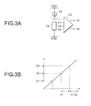
- the select signal generation circuit is used as the sensing means sensing the variation in load resistance (load resistance of the delay elements 12 in VCDLs 2 to 4, load resistance in CT part 6, or the resistance element described below).
- the construction is formed by a resistance element 13 having the same shape as the load resistance; a constant current source 12 supplying a constant current (a constant current not depending on resistance element 13) to resistance element 13; and a Schmidt comparator 14 comparing potential VCONT of the junction of resistance element 13 and constant current source 12 with threshold voltages V1, V2 and V3 (V3 > V2 > V1) as reference voltages having different values to output select signals S1, S2.
- the VCONT is positioned between reference threshold voltages V1 and V2 and the delay time of clock tree part 6 and VCDLs 2 to 4 indicates a small value.
- select signals S1, S2 are both on and the VCDLs 2 to 4 are all operated to change the clock into the lock state.
- the VCONT is positioned between reference threshold voltages V2 and V3 and the delay time of clock tree part 6 and VCDLs 2 to 4 indicates an almost center value. At this time, only the select signal S1 is off and the VCDLs 2 and 3 are operated to change the clock into the lock state.
- the VCONT is positioned above the reference threshold potential V3 and the delay time of clock tree part 6 and
- VCDLs 2 to 4 indicates a large value.
- the select signals S1, S2 are both off and only VCDL 2 is operated to change the clock into the lock state.
- Schmidt comparator 14 is used in a high-speed differential common mode logic (CML) circuit.
- the high-resistance polysilicon often used in the high-speed differential CML circuit has a very low temperature dependence.
- the resistance value of the resistance element once manufactured indicates an almost constant value during operation.
- a Schmidt circuit is provided so as to prevent the value of the potential VCONT from exceeding threshold voltages V2, V3 due to the influence of noise.
- select signals S1, S2 are prevented from being turned on unless the potential VCONT is below threshold voltage V1.
- noise margin can be increased.
- the delay locked loop of the present invention determines, upon power-on, the basic number of the plurality of VCDLs provided depending on the resistance value variation of the resistance loads.
- the delay variation width of the VCDL is small, the clock of the clock tree (CT) part can be locked within the variation range .
- CT clock tree
- the resistance value variation of the resistance loads of the VCDLs is sensed, and then, the basic number of the VCDLs is determined corresponding to the variation to lock the clock. Even when the delay variation width of the VCDLs is small, malfunction can be prevented.
Landscapes
- Engineering & Computer Science (AREA)
- Theoretical Computer Science (AREA)
- Physics & Mathematics (AREA)
- General Engineering & Computer Science (AREA)
- General Physics & Mathematics (AREA)
- Stabilization Of Oscillater, Synchronisation, Frequency Synthesizers (AREA)
- Pulse Circuits (AREA)
- Synchronisation In Digital Transmission Systems (AREA)
Abstract
Description
As shown in FIG. 5, the rising edge of the clock (B) to be synchronized with the data (C) after one cycle of the reception clock (A) is a lock point (LP) via the
As shown in FIG. 2, as in FIG. 5, the clock (B) delayed in one cycle (800 picoseconds) from the rising of the clock (A) received by
As shown in FIG. 3A, the select signal generation circuit is used as the sensing means sensing the variation in load resistance (load resistance of the
Claims (4)
- A delay locked loop which synthesizes data and a clock inputted from outside comprising:voltage control delay loops having a plurality of delay circuit parts sequentially delaying said clock;a slot selector selecting a slot outputted from the delay circuit parts of said voltage control delay loops;a clock tree part creating a plurality of clocks with the same timing by an output of said slot selector;a phase control part phase-controlling said plurality of delay circuit parts corresponding to the output clock delay variation of said clock tree part; andsensing means on-off controlling all or part of said plurality of delay circuit parts and said slot selector.
- The delay locked loop according to claim 1, wherein said plurality of delay circuit parts is formed by connecting a plurality of delay elements in series.
- The loop according to claims 1 or 2, wherein said phase control part controls said plurality of delay circuit parts of said voltage control delay loops in a group unit.
- The loop according to any one of claims 1 to 3, wherein said sensing means is formed by a select signal generation circuit having resistance element means having one end connected to a first power source and formed to be the same shape as the resistance element of said voltage control delay loop and said clock tree part; a constant current source connected between a second power source and the other end of said resistance element means; and a Schmidt circuit having, as one input, a junction potential of said resistance element means and said constant current source, supplying threshold voltages having a plurality of reference potentials to the other input, and outputting a plurality of select signals by the comparison result.
Applications Claiming Priority (2)
| Application Number | Priority Date | Filing Date | Title |
|---|---|---|---|
| JP2001281115A JP4522623B2 (en) | 2001-09-17 | 2001-09-17 | Delay control device |
| JP2001281115 | 2001-09-17 |
Publications (3)
| Publication Number | Publication Date |
|---|---|
| EP1294101A2 true EP1294101A2 (en) | 2003-03-19 |
| EP1294101A3 EP1294101A3 (en) | 2004-08-04 |
| EP1294101B1 EP1294101B1 (en) | 2006-08-23 |
Family
ID=19105002
Family Applications (1)
| Application Number | Title | Priority Date | Filing Date |
|---|---|---|---|
| EP02090333A Expired - Lifetime EP1294101B1 (en) | 2001-09-17 | 2002-09-14 | Delay locked loop |
Country Status (4)
| Country | Link |
|---|---|
| US (1) | US7164743B2 (en) |
| EP (1) | EP1294101B1 (en) |
| JP (1) | JP4522623B2 (en) |
| DE (1) | DE60214100T2 (en) |
Cited By (1)
| Publication number | Priority date | Publication date | Assignee | Title |
|---|---|---|---|---|
| US7084682B2 (en) | 2003-10-31 | 2006-08-01 | Samsung Electronics, Co., Ltd. | Delay-locked loop circuit and method thereof for generating a clock signal |
Families Citing this family (7)
| Publication number | Priority date | Publication date | Assignee | Title |
|---|---|---|---|---|
| JP3759134B2 (en) * | 2003-08-29 | 2006-03-22 | ローム株式会社 | Power supply |
| US7443905B1 (en) * | 2004-03-19 | 2008-10-28 | National Semiconductor Corporation | Apparatus and method for spread spectrum clock generator with accumulator |
| JP4774005B2 (en) * | 2007-04-11 | 2011-09-14 | ザインエレクトロニクス株式会社 | Receiver |
| KR100892684B1 (en) | 2007-11-09 | 2009-04-15 | 주식회사 하이닉스반도체 | Data Center Tracking Circuits and Semiconductor Integrated Circuits Containing the Same |
| US8116540B2 (en) * | 2008-04-04 | 2012-02-14 | Validity Sensors, Inc. | Apparatus and method for reducing noise in fingerprint sensing circuits |
| JP5807550B2 (en) * | 2012-01-10 | 2015-11-10 | 株式会社ソシオネクスト | Semiconductor device |
| US9477258B2 (en) | 2013-05-22 | 2016-10-25 | Industrial Technology Research Institute | Clock tree in circuit having a power-mode control circuit to determine a first delay time and a second delay time |
Family Cites Families (7)
| Publication number | Priority date | Publication date | Assignee | Title |
|---|---|---|---|---|
| US3558933A (en) * | 1968-05-01 | 1971-01-26 | Ampex | Voltage variable delay line termination |
| JP3639000B2 (en) * | 1995-06-13 | 2005-04-13 | 富士通株式会社 | Phase matching device and delay control circuit |
| KR100295052B1 (en) * | 1998-09-02 | 2001-07-12 | 윤종용 | Delay locked loop including a controller capable of changing a number of unit delay in voltage controlled delay line |
| FR2792760B1 (en) * | 1999-04-23 | 2001-08-17 | St Microelectronics Sa | OPTIMIZED SETTING MEMORY OF PRELOADING MOMENTS |
| JP2000357951A (en) * | 1999-06-15 | 2000-12-26 | Mitsubishi Electric Corp | Delay circuit, clock generation circuit, and phase synchronization circuit |
| US6275555B1 (en) * | 1999-12-30 | 2001-08-14 | Intel Corporation | Digital delay locked loop for adaptive de-skew clock generation |
| JP3865191B2 (en) * | 2000-02-21 | 2007-01-10 | 株式会社ルネサステクノロジ | Semiconductor integrated circuit device |
-
2001
- 2001-09-17 JP JP2001281115A patent/JP4522623B2/en not_active Expired - Fee Related
-
2002
- 2002-09-12 US US10/241,515 patent/US7164743B2/en not_active Expired - Lifetime
- 2002-09-14 EP EP02090333A patent/EP1294101B1/en not_active Expired - Lifetime
- 2002-09-14 DE DE60214100T patent/DE60214100T2/en not_active Expired - Lifetime
Cited By (1)
| Publication number | Priority date | Publication date | Assignee | Title |
|---|---|---|---|---|
| US7084682B2 (en) | 2003-10-31 | 2006-08-01 | Samsung Electronics, Co., Ltd. | Delay-locked loop circuit and method thereof for generating a clock signal |
Also Published As
| Publication number | Publication date |
|---|---|
| DE60214100D1 (en) | 2006-10-05 |
| JP2003087114A (en) | 2003-03-20 |
| EP1294101A3 (en) | 2004-08-04 |
| JP4522623B2 (en) | 2010-08-11 |
| US20030053577A1 (en) | 2003-03-20 |
| US7164743B2 (en) | 2007-01-16 |
| EP1294101B1 (en) | 2006-08-23 |
| DE60214100T2 (en) | 2007-04-12 |
Similar Documents
| Publication | Publication Date | Title |
|---|---|---|
| KR100527397B1 (en) | Delay Locked Loop having small jitter in semiconductor memory device | |
| US6392456B1 (en) | Analog mixed digital DLL | |
| US6642760B1 (en) | Apparatus and method for a digital delay locked loop | |
| US7839177B1 (en) | Techniques for phase detection with fast reset | |
| US20020079937A1 (en) | Digital delay locked loop with wide dynamic range and fine precision | |
| KR100733471B1 (en) | Delayed fixed loop circuit of semiconductor memory device and its control method | |
| US20030151433A1 (en) | Semiconductor integrated circuit device and delay-locked loop device | |
| US6882196B2 (en) | Duty cycle corrector | |
| US20070069780A1 (en) | Delay cell of voltage controlled delay line using digital and analog control scheme | |
| JPH11145816A (en) | Semiconductor device | |
| EP1294101A2 (en) | Delay locked loop | |
| US20040135605A1 (en) | Delay locked loops having delay time compensation and methods for compensating for delay time of the delay locked loops | |
| US6809555B1 (en) | Glitch-free digital phase detector circuits and methods with optional offset and lock window extension | |
| US7808289B2 (en) | Method and apparatus for digital phase generation for high frequency clock applications | |
| US6756808B2 (en) | Clock edge detection circuit | |
| Liu et al. | Low-power clock-deskew buffer for high-speed digital circuits | |
| US7248091B2 (en) | Semiconductor device having delay drift compensation circuit that compensates for delay drift caused by temperature and voltage variations in clock tree | |
| US7158600B2 (en) | Charge pump phase locked loop | |
| US20070216456A1 (en) | Delay locked loop and method of locking a clock signal | |
| US7157951B1 (en) | Digital clock manager capacitive trim unit | |
| US9742413B2 (en) | Electronic device and information processing apparatus | |
| WO2005008894A1 (en) | Delay locked loop for generating multi-phase clocks without voltage-controlled oscillator | |
| US6232813B1 (en) | Phase locked loop integrated circuits having fuse-enabled and fuse-disabled delay devices therein | |
| US20070273416A1 (en) | Signal delay loop and method for locking a signal delay loop | |
| US7911859B2 (en) | Delay line and memory control circuit utilizing the delay line |
Legal Events
| Date | Code | Title | Description |
|---|---|---|---|
| PUAI | Public reference made under article 153(3) epc to a published international application that has entered the european phase |
Free format text: ORIGINAL CODE: 0009012 |
|
| AK | Designated contracting states |
Kind code of ref document: A2 Designated state(s): AT BE BG CH CY CZ DE DK EE ES FI FR GB GR IE IT LI LU MC NL PT SE SK TR |
|
| AX | Request for extension of the european patent |
Extension state: AL LT LV MK RO SI |
|
| RAP1 | Party data changed (applicant data changed or rights of an application transferred) |
Owner name: NEC ELECTRONICS CORPORATION |
|
| PUAL | Search report despatched |
Free format text: ORIGINAL CODE: 0009013 |
|
| AK | Designated contracting states |
Kind code of ref document: A3 Designated state(s): AT BE BG CH CY CZ DE DK EE ES FI FR GB GR IE IT LI LU MC NL PT SE SK TR |
|
| AX | Request for extension of the european patent |
Extension state: AL LT LV MK RO SI |
|
| 17P | Request for examination filed |
Effective date: 20040806 |
|
| AKX | Designation fees paid |
Designated state(s): DE GB |
|
| RBV | Designated contracting states (corrected) |
Designated state(s): DE GB |
|
| GRAP | Despatch of communication of intention to grant a patent |
Free format text: ORIGINAL CODE: EPIDOSNIGR1 |
|
| GRAS | Grant fee paid |
Free format text: ORIGINAL CODE: EPIDOSNIGR3 |
|
| GRAA | (expected) grant |
Free format text: ORIGINAL CODE: 0009210 |
|
| AK | Designated contracting states |
Kind code of ref document: B1 Designated state(s): DE GB |
|
| REG | Reference to a national code |
Ref country code: GB Ref legal event code: FG4D |
|
| REF | Corresponds to: |
Ref document number: 60214100 Country of ref document: DE Date of ref document: 20061005 Kind code of ref document: P |
|
| PLBE | No opposition filed within time limit |
Free format text: ORIGINAL CODE: 0009261 |
|
| STAA | Information on the status of an ep patent application or granted ep patent |
Free format text: STATUS: NO OPPOSITION FILED WITHIN TIME LIMIT |
|
| 26N | No opposition filed |
Effective date: 20070524 |
|
| PGFP | Annual fee paid to national office [announced via postgrant information from national office to epo] |
Ref country code: GB Payment date: 20080917 Year of fee payment: 7 |
|
| GBPC | Gb: european patent ceased through non-payment of renewal fee |
Effective date: 20090914 |
|
| PG25 | Lapsed in a contracting state [announced via postgrant information from national office to epo] |
Ref country code: GB Free format text: LAPSE BECAUSE OF NON-PAYMENT OF DUE FEES Effective date: 20090914 |
|
| REG | Reference to a national code |
Ref country code: DE Ref legal event code: R082 Ref document number: 60214100 Country of ref document: DE Representative=s name: STORK BAMBERGER PATENTANWAELTE, DE |
|
| REG | Reference to a national code |
Ref country code: DE Ref legal event code: R082 Ref document number: 60214100 Country of ref document: DE Representative=s name: STORK BAMBERGER PATENTANWAELTE PARTMBB, DE Effective date: 20120828 Ref country code: DE Ref legal event code: R082 Ref document number: 60214100 Country of ref document: DE Representative=s name: STORK BAMBERGER PATENTANWAELTE, DE Effective date: 20120828 Ref country code: DE Ref legal event code: R081 Ref document number: 60214100 Country of ref document: DE Owner name: RENESAS ELECTRONICS CORPORATION, JP Free format text: FORMER OWNER: NEC ELECTRONICS CORP., KAWASAKI, JP Effective date: 20120828 Ref country code: DE Ref legal event code: R081 Ref document number: 60214100 Country of ref document: DE Owner name: RENESAS ELECTRONICS CORPORATION, KAWASAKI-SHI, JP Free format text: FORMER OWNER: NEC ELECTRONICS CORP., KAWASAKI, KANAGAWA, JP Effective date: 20120828 |
|
| PGFP | Annual fee paid to national office [announced via postgrant information from national office to epo] |
Ref country code: DE Payment date: 20150908 Year of fee payment: 14 |
|
| REG | Reference to a national code |
Ref country code: DE Ref legal event code: R119 Ref document number: 60214100 Country of ref document: DE |
|
| PG25 | Lapsed in a contracting state [announced via postgrant information from national office to epo] |
Ref country code: DE Free format text: LAPSE BECAUSE OF NON-PAYMENT OF DUE FEES Effective date: 20170401 |