EP1294087A2 - Power supply - Google Patents
Power supply Download PDFInfo
- Publication number
- EP1294087A2 EP1294087A2 EP02102133A EP02102133A EP1294087A2 EP 1294087 A2 EP1294087 A2 EP 1294087A2 EP 02102133 A EP02102133 A EP 02102133A EP 02102133 A EP02102133 A EP 02102133A EP 1294087 A2 EP1294087 A2 EP 1294087A2
- Authority
- EP
- European Patent Office
- Prior art keywords
- power supply
- capacitor
- terminal
- potential
- rectifier
- Prior art date
- Legal status (The legal status is an assumption and is not a legal conclusion. Google has not performed a legal analysis and makes no representation as to the accuracy of the status listed.)
- Granted
Links
- 239000003990 capacitor Substances 0.000 claims abstract description 44
- 230000000630 rising effect Effects 0.000 claims abstract description 13
- 230000008878 coupling Effects 0.000 claims description 6
- 238000010168 coupling process Methods 0.000 claims description 6
- 238000005859 coupling reaction Methods 0.000 claims description 6
- 238000013021 overheating Methods 0.000 claims description 6
- 238000010586 diagram Methods 0.000 description 3
- 230000001131 transforming effect Effects 0.000 description 3
- 238000010438 heat treatment Methods 0.000 description 2
- 238000004804 winding Methods 0.000 description 2
- 230000003750 conditioning effect Effects 0.000 description 1
- 238000000034 method Methods 0.000 description 1
- 230000001105 regulatory effect Effects 0.000 description 1
- 239000007787 solid Substances 0.000 description 1
- 230000005236 sound signal Effects 0.000 description 1
Images


Classifications
-
- H—ELECTRICITY
- H02—GENERATION; CONVERSION OR DISTRIBUTION OF ELECTRIC POWER
- H02M—APPARATUS FOR CONVERSION BETWEEN AC AND AC, BETWEEN AC AND DC, OR BETWEEN DC AND DC, AND FOR USE WITH MAINS OR SIMILAR POWER SUPPLY SYSTEMS; CONVERSION OF DC OR AC INPUT POWER INTO SURGE OUTPUT POWER; CONTROL OR REGULATION THEREOF
- H02M1/00—Details of apparatus for conversion
- H02M1/42—Circuits or arrangements for compensating for or adjusting power factor in converters or inverters
- H02M1/4208—Arrangements for improving power factor of AC input
-
- H—ELECTRICITY
- H02—GENERATION; CONVERSION OR DISTRIBUTION OF ELECTRIC POWER
- H02M—APPARATUS FOR CONVERSION BETWEEN AC AND AC, BETWEEN AC AND DC, OR BETWEEN DC AND DC, AND FOR USE WITH MAINS OR SIMILAR POWER SUPPLY SYSTEMS; CONVERSION OF DC OR AC INPUT POWER INTO SURGE OUTPUT POWER; CONTROL OR REGULATION THEREOF
- H02M7/00—Conversion of AC power input into DC power output; Conversion of DC power input into AC power output
- H02M7/02—Conversion of AC power input into DC power output without possibility of reversal
- H02M7/04—Conversion of AC power input into DC power output without possibility of reversal by static converters
- H02M7/12—Conversion of AC power input into DC power output without possibility of reversal by static converters using discharge tubes with control electrode or semiconductor devices with control electrode
- H02M7/21—Conversion of AC power input into DC power output without possibility of reversal by static converters using discharge tubes with control electrode or semiconductor devices with control electrode using devices of a triode or transistor type requiring continuous application of a control signal
- H02M7/217—Conversion of AC power input into DC power output without possibility of reversal by static converters using discharge tubes with control electrode or semiconductor devices with control electrode using devices of a triode or transistor type requiring continuous application of a control signal using semiconductor devices only
-
- H—ELECTRICITY
- H02—GENERATION; CONVERSION OR DISTRIBUTION OF ELECTRIC POWER
- H02M—APPARATUS FOR CONVERSION BETWEEN AC AND AC, BETWEEN AC AND DC, OR BETWEEN DC AND DC, AND FOR USE WITH MAINS OR SIMILAR POWER SUPPLY SYSTEMS; CONVERSION OF DC OR AC INPUT POWER INTO SURGE OUTPUT POWER; CONTROL OR REGULATION THEREOF
- H02M1/00—Details of apparatus for conversion
- H02M1/32—Means for protecting converters other than automatic disconnection
-
- Y—GENERAL TAGGING OF NEW TECHNOLOGICAL DEVELOPMENTS; GENERAL TAGGING OF CROSS-SECTIONAL TECHNOLOGIES SPANNING OVER SEVERAL SECTIONS OF THE IPC; TECHNICAL SUBJECTS COVERED BY FORMER USPC CROSS-REFERENCE ART COLLECTIONS [XRACs] AND DIGESTS
- Y02—TECHNOLOGIES OR APPLICATIONS FOR MITIGATION OR ADAPTATION AGAINST CLIMATE CHANGE
- Y02B—CLIMATE CHANGE MITIGATION TECHNOLOGIES RELATED TO BUILDINGS, e.g. HOUSING, HOUSE APPLIANCES OR RELATED END-USER APPLICATIONS
- Y02B70/00—Technologies for an efficient end-user side electric power management and consumption
- Y02B70/10—Technologies improving the efficiency by using switched-mode power supplies [SMPS], i.e. efficient power electronics conversion e.g. power factor correction or reduction of losses in power supplies or efficient standby modes
Definitions
- a power supply includes a capacitor, having a first terminal and a second terminal, for storing DC charge.
- the power supply also includes first and second line input terminals for connecting to a source of AC line current, the AC line current having an AC line voltage, a transformer, coupled to the first and second line input terminals, for transforming the AC line voltage to a reduced AC voltage, a rectifier, coupled to the transformer, for rectifying the reduced AC voltage to rectified AC, the rectified AC having a voltage waveform having a rising edge, a falling edge, and a peak.
- the power supply also includes charging circuitry, coupling the rectifier and the capacitor, for charging the capacitor to a nominal DC output voltage.
- the power supply is constructed and arranged so that the charging circuitry charges the capacitor during an interval during the rising edge and during an interval during the falling edge, and so that the charging circuitry does not charge the capacitor at the peak.
- a power supply in another aspect of the invention, includes a first, second, and third output terminal and first and second line input terminals for connecting to a source of AC line current, the AC line current having an AC line voltage.
- the power supply further includes a transformer, coupled to the first and second line input terminals, for transforming the AC line voltage to a reduced AC voltage; a rectifier, coupled to the transformer, for rectifying the reduced AC voltage to rectified AC; and charging circuitry, for charging the first, second, and third output terminals to a first, second, and third electrical potential, respectively, so a potential difference between the first potential and the second potential is less than a potential difference between the first potential and the third potential.
- the charging circuitry includes a single switch.
- a power supply in still another aspect of the invention, includes a capacitor, having a first terminal and a second terminal, for storing DC charge.
- the power supply also includes first and second line input terminals for connecting to a source of AC line current, the AC line current having an AC line voltage, a transformer, coupled to the first and second line input terminals, for transforming the AC line voltage to a reduced AC voltage, a rectifier, coupled to the transformer, for rectifying the reduced AC voltage to rectified AC, the rectified AC having a voltage waveform having a rising edge, a falling edge, and a peak.
- the power supply also includes charging circuitry, coupling the rectifier and the capacitor, for charging the capacitor to a nominal DC output voltage. The power supply is constructed and arranged so that the charging circuitry charges the capacitor twice during each rectified AC cycle.
- a power supply includes power supply input terminals 10, 11, for connecting to an external AC power source, such as 120V 60Hz line power. Power supply input terminals 10, 11, are connected to primary winding of transformer 12.
- Switch circuit 32 includes reference block 34, control block 36, and switch 38. Inputs of reduced voltage circuit 40 are coupled to an intermediate voltage tap of transformer 12 and terminal 28 of load capacitor 26.
- Reference block 34 receives signals from high side power line 21, low side power line 23, terminal 28 of load capacitor 26, and thermal sensing circuit 44. Reference block 34 transmits signals to control block 36, which controls switch 38.
- a power supply according to the invention having a switch on the low side power line is advantageous over power supplies having switches on the high side power line because there is less switching loss (dissipated as heat) when the switch is on the low side power line.
- transformer 12 converts the input voltage from line AC voltage level (e.g. 120V. 60Hz) to an intermediate AC voltage level (such as 17V. 60Hz).
- Rectifier 14 rectifies the intermediate voltage AC to rectified AC voltage, which is then used to charge capacitor 26, which maintains a DC voltage across load, represented by load resistor R L 30.
- Switch circuit 32 controls the charging of capacitor 26 as described below.
- Transformer 12, rectifier 14, and capacitor 26 are conventional elements.
- Switch 38 may be a conventional n-type MOSFET switch.
- Load represented by load resistor R L 30 is typically a circuit requiring DC power, such as audio signal processing circuitry and a power amplifier.
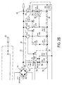
- FIG. 2 there is shown a circuit for implementing the power supply of FIG. 1.
- Like reference numbers in FIG. 2 refer to corresponding elements of FIG. 1.
- Dashed line boxes in FIG. 2 enclose the portions of the circuit that perform the functions represented by the blocks of FIG. 1.
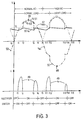
- Curve 50 is a plot of voltage V ac , the voltage across the input lines to rectifier terminals 16, 18. The perturbations in curve 50 are due to the load when the power supply is charging.
- Curve 51 is a plot of V i , the voltage across the output terminals 20, 22 of the rectifier.
- Curve 53 is a plot of V z , the voltage between nodes 54 and 22.
- Curve 57 for reference, is a waveform of the rectified value of V ac, if it were operating without a load.
- Curve 55 is a plot of V o , the voltage across terminals 24, 28 of load capacitor 26.
- Curve 55 has an upward slope when load capacitor 26 is being charged and a downward slope when capacitor 26 discharges through load resistor 30.
- Curve 49 is a plot of I s , the charging current, illustrating when capacitor 26 is being charged. The curves have been smoothed, that is minor perturbations and voltage spikes due to switching are not shown.
- Load capacitor is being charged when switch 38 is in the ON position and when rectifier 14 is ON (that is, when the voltage across input terminals 16, 18 is less than the voltage across the rectifier output terminals 20, 22, causing current to flow through rectifier 14).
- switch 38 The operation of switch 38 is understood by reference to curves 51 and 53.
- Switch is initially ON at time t 0 .
- switch 38 turns OFF when V i is equal to V t .
- Switch 38 turns ON at time t 3 on the falling edge of the cycle, when V z is greater than V t by an amount V z , which is determined by the characteristics of transformer 12 and the ratio of resistors 70 and 72.
- Switch 38 remains ON through time t 5 , which is essentially equivalent to time t 0 .
- Switch 38 turns OFF at time t 12 on the following half cycle, essentially similar to the situation at time t 2 , and turns ON at time t 13 , which is essentially similar to the situation at time t 14 .
- Rectifier 14 turns ON at time t 1 , when V i becomes greater than V o .
- Rectifier 14 turns OFF at time t 4 , when V i becomes less than V o .
- Rectifier 14 remains OFF through time t 5 , which is essentially equivalent to time t 0 .
- Rectifier 14 turns ON again at time t 11 , which is essentially similar to the situation at time t 1 .
- Rectifier 14 turns OFF at time t 14 , which is essentially similar to the situation at time t 4 .
- Rectifier 14 and switch 38 are both ON during one interval (t 1 to t 2 ) on the rising edge of the first half cycle and during one interval (t 3 to t 4 ) on the falling edge of the first half cycle.
- rectifier 14 and switch 38 are both ON during one interval (t 11 to t 12 ) on the rising edge of the second half cycle and during one interval (t 13 to t 14 ) on the falling edge of the second half cycle.
- the power supply is being charged during one interval on the rising edge of the half cycle and during one interval on the falling edge of the half cycle.
- the power supply is not being charged during the interval that includes the peak 65 of the half cycle.
- the length of the charging intervals (t 1 to t 2 ), (t 3 to t 4 ), (t 11 to t 12 ), (t 13 to t 14 ) is determined by a number of factors, including the shape of the input waveform (which may not be purely sinusoidal if the power line is loaded with a large number of devices that draw power near the peak of the AC cycle), the load on the power supply, and characteristics of transformer 12 and the ratio of the two resistors 70 and 72 of FIG. 2.
- the power supply operates as described over a wide range of typical conditions, including variations in V ac and load.
- the interval t 5 to t 15 shows that the power supply according to the invention maintains a maximum voltage at V t even with a high AC voltage and a light load.
- a power supply according to the invention generally is subject to less agency regulation (such as EMC standard EN61000, which has a special class for power supplies such as the present one, which require less or no line conditioning devices for power factor correction). Furthermore, a power supply according to the invention can pass easily many EMI standards such as FCC and line conducted emissions) because of the lack of high frequency switching.
- EMC standard EN61000 which has a special class for power supplies such as the present one, which require less or no line conditioning devices for power factor correction.
- a power supply according to the invention can pass easily many EMI standards such as FCC and line conducted emissions) because of the lack of high frequency switching.
- a power supply that does not charge at the peak is advantageous because the output voltage has a fixed maximum which does not change, even though the line voltage varies, as long as the peak of V ac is greater than V t .
- a power supply that charges twice (or more) during each half line AC cycle or four times (or more) during each full line AC cycle maintains a voltage close to the intended output voltage under heavy load conditions than does a power supply that charges only once per half cycle or twice per full cycle.
- the falling edge charging generates less switch heating than rising edge charging, so the inclusion of falling edge charging means less overall switch heating for the same load.
- reduced voltage circuit 40 of FIG. 1 is implemented as a diode 74 coupled to an intermediate voltage tap of transformer, capacitor 76, reduced voltage terminal 42, and to capacitor terminal 28 through capacitor 28.
- Voltage at terminal 42 may be used to power devices having voltage requirements less than the devices represented by the resistor R L 30.
- terminals 24, 42, and 28 can be configured as terminals with voltages at + V o / 2, ground, and - V o / 2, respectively. In such a configuration, a power supply according to the invention could be used to power bipolar devices
- a power supply according to the invention is advantageous over power supplies using duplicate functionally similar circuits to derive reduced voltage or bipolar voltages, because a power supply according to the invention requires fewer components, such as load capacitors, switches, and switch control circuits, reducing circuit cost.
- a power supply according to the invention requires less expensive components and can operate at higher power levels than power supplies providing reduced voltages using regulators.
- thermal sensing circuit 44 of FIG. 1 is implemented as a negative temperature coefficient (NTC) resistor 46 embedded in transformer 12 and coupled to the reference circuit terminal node 54 and low side power line 23 by resistor 60.
- NTC negative temperature coefficient
- This NTC resistor and additional thermistors can be placed elsewhere in the circuit to protect other critically hot components.
- a power supply including a thermal sensing circuit 44 is advantageous over power supplies employing power fusing resistors because the power supply continues to operate (at reduced output) during overheating conditions rather than failing catastrophically. When the overheating condition no longer exists, the power supply resumes normal operation at full power. In most applications, especially high power applications, a power supply with a transformer is more efficient than a power supply with a power resistor as the voltage reducing element.
- FIGS. 1 and 2 employs a bridge rectifier 14, the invention may also be implemented in a power supply employing other forms of rectifiers, such as a diode rectifier or equivalent, and the circuit could be adapted to the rectifier employed.
- a single diode rectifier could be used to provide half wave rectified AC. During each half wave, there would be charging during an interval during the rising edge and during an interval during the falling edge, and no charging at other parts of the waveform including the portion of the waveform between the rising edge charging and the falling edge charging.
Landscapes
- Engineering & Computer Science (AREA)
- Power Engineering (AREA)
- Rectifiers (AREA)
- Dc-Dc Converters (AREA)
- Apparatus For Radiation Diagnosis (AREA)
- Control Of Electrical Variables (AREA)
Abstract
Description
- It is an important object of the invention to provide a high power partially regulated power supply using line frequency switching circuitry and having low switching loss and thermal protection.
- According to the invention, a power supply includes a capacitor, having a first terminal and a second terminal, for storing DC charge. The power supply also includes first and second line input terminals for connecting to a source of AC line current, the AC line current having an AC line voltage, a transformer, coupled to the first and second line input terminals, for transforming the AC line voltage to a reduced AC voltage, a rectifier, coupled to the transformer, for rectifying the reduced AC voltage to rectified AC, the rectified AC having a voltage waveform having a rising edge, a falling edge, and a peak. The power supply also includes charging circuitry, coupling the rectifier and the capacitor, for charging the capacitor to a nominal DC output voltage. The power supply is constructed and arranged so that the charging circuitry charges the capacitor during an interval during the rising edge and during an interval during the falling edge, and so that the charging circuitry does not charge the capacitor at the peak.
- In another aspect of the invention, a power supply, includes a first, second, and third output terminal and first and second line input terminals for connecting to a source of AC line current, the AC line current having an AC line voltage. The power supply further includes a transformer, coupled to the first and second line input terminals, for transforming the AC line voltage to a reduced AC voltage; a rectifier, coupled to the transformer, for rectifying the reduced AC voltage to rectified AC; and charging circuitry, for charging the first, second, and third output terminals to a first, second, and third electrical potential, respectively, so a potential difference between the first potential and the second potential is less than a potential difference between the first potential and the third potential. The charging circuitry includes a single switch.
- In still another aspect of the invention, a power supply includes a capacitor, having a first terminal and a second terminal, for storing DC charge. The power supply also includes first and second line input terminals for connecting to a source of AC line current, the AC line current having an AC line voltage, a transformer, coupled to the first and second line input terminals, for transforming the AC line voltage to a reduced AC voltage, a rectifier, coupled to the transformer, for rectifying the reduced AC voltage to rectified AC, the rectified AC having a voltage waveform having a rising edge, a falling edge, and a peak. The power supply also includes charging circuitry, coupling the rectifier and the capacitor, for charging the capacitor to a nominal DC output voltage. The power supply is constructed and arranged so that the charging circuitry charges the capacitor twice during each rectified AC cycle.
- Other features, objects, and advantages will become apparent from the following detailed description, which refers to the accompanying drawing in which:
- FIG. 1 is a block diagram of a power supply according to the invention;
- FIG. 2 is a schematic diagram of a power supply according to FIG. 1; and
- FIG. 3 shows waveforms and other electrical parameters, illustrating the operation of the power supply of FIGS. 1 and 2.
-
- With reference now to the drawing and more particularly to FIG. 1, there is shown a block diagram of the logical arrangement of a power supply according to the invention. The lines connecting the elements are shown as solid or dashed. Solid lines represent interconnection between elements for transmitting electrical power. Dashed lines connecting elements represent interconnection between elements for the transmitting information or control; the arrows on the dashed lines represent the direction of the flow of information or control. For the sake of clarity, interconnections for powering or grounding circuit devices are not shown in this view, but are shown in FIG. 2. A power supply includes power
supply input terminals 10, 11, for connecting to an external AC power source, such as 120V 60Hz line power. Powersupply input terminals 10, 11, are connected to primary winding oftransformer 12. Secondary windings oftransformer 12 are coupled to rectifier 14 throughrectifier input terminals positive output terminal 20 is coupled by highside power line 21 toterminal 24 ofload capacitor 26.Load resistor R L 30 is coupled in parallel withcapacitor 26 atterminals negative terminal 22 is coupled toterminal 28 ofcapacitor 26 andload resistor R L 30 throughswitch circuit 32.Switch circuit 32 includesreference block 34,control block 36, andswitch 38. Inputs of reducedvoltage circuit 40 are coupled to an intermediate voltage tap oftransformer 12 andterminal 28 ofload capacitor 26.Reference block 34 receives signals from highside power line 21, lowside power line 23,terminal 28 ofload capacitor 26, andthermal sensing circuit 44.Reference block 34 transmits signals to controlblock 36, which controlsswitch 38. - A power supply according to the invention having a switch on the low side power line is advantageous over power supplies having switches on the high side power line because there is less switching loss (dissipated as heat) when the switch is on the low side power line.
- In operation,
transformer 12 converts the input voltage from line AC voltage level (e.g. 120V. 60Hz) to an intermediate AC voltage level (such as 17V. 60Hz). Rectifier 14 rectifies the intermediate voltage AC to rectified AC voltage, which is then used to chargecapacitor 26, which maintains a DC voltage across load, represented byload resistor R L 30. Switchcircuit 32 controls the charging ofcapacitor 26 as described below. - Transformer 12,
rectifier 14, andcapacitor 26 are conventional elements. Switch 38 may be a conventional n-type MOSFET switch. Load represented byload resistor R L 30 is typically a circuit requiring DC power, such as audio signal processing circuitry and a power amplifier. - Referring now to FIG. 2, there is shown a circuit for implementing the power supply of FIG. 1. Like reference numbers in FIG. 2 refer to corresponding elements of FIG. 1. Dashed line boxes in FIG. 2 enclose the portions of the circuit that perform the functions represented by the blocks of FIG. 1.
- Referring now to FIG. 3, there is shown a plot of voltages and charging current for the purpose of illustrating the operation of the power supply of FIGS. 1 and 2.
Curve 50 is a plot of voltage Vac, the voltage across the input lines torectifier terminals curve 50 are due to the load when the power supply is charging. Curve 51 is a plot of Vi, the voltage across theoutput terminals Curve 53 is a plot of Vz, the voltage betweennodes Curve 57, for reference, is a waveform of the rectified value of Vac, if it were operating without a load.Curve 55 is a plot of Vo, the voltage acrossterminals load capacitor 26.Curve 55 has an upward slope whenload capacitor 26 is being charged and a downward slope whencapacitor 26 discharges throughload resistor 30.Curve 49 is a plot of Is, the charging current, illustrating whencapacitor 26 is being charged. The curves have been smoothed, that is minor perturbations and voltage spikes due to switching are not shown. - Load capacitor is being charged when
switch 38 is in the ON position and whenrectifier 14 is ON (that is, when the voltage acrossinput terminals rectifier output terminals - The operation of
switch 38 is understood by reference tocurves 51 and 53. Switch is initially ON at time t0. At time t2,switch 38 turns OFF when Vi is equal to Vt. Switch 38 turns ON at time t3 on the falling edge of the cycle, when Vz is greater than Vt by an amount Vz, which is determined by the characteristics oftransformer 12 and the ratio of resistors 70 and 72.Switch 38 remains ON through time t5, which is essentially equivalent to time t0. Switch 38 turns OFF at time t12 on the following half cycle, essentially similar to the situation at time t2, and turns ON at time t13, which is essentially similar to the situation at time t14. Rectifier 14 turns ON at time t1, when Vi becomes greater than Vo. Rectifier 14 turns OFF at time t4, when Vi becomes less than Vo. Rectifier 14 remains OFF through time t5, which is essentially equivalent to time t0. Rectifier 14 turns ON again at time t11, which is essentially similar to the situation at time t1. Rectifier 14 turns OFF at time t14, which is essentially similar to the situation at time t4. - Rectifier 14 and
switch 38 are both ON during one interval (t1 to t2) on the rising edge of the first half cycle and during one interval (t3 to t4) on the falling edge of the first half cycle. Similarly,rectifier 14 andswitch 38 are both ON during one interval (t11 to t12) on the rising edge of the second half cycle and during one interval (t13 to t14) on the falling edge of the second half cycle. Thus, the power supply is being charged during one interval on the rising edge of the half cycle and during one interval on the falling edge of the half cycle. The power supply is not being charged during the interval that includes thepeak 65 of the half cycle. The length of the charging intervals (t1 to t2), (t3 to t4), (t11 to t12), (t13 to t14) is determined by a number of factors, including the shape of the input waveform (which may not be purely sinusoidal if the power line is loaded with a large number of devices that draw power near the peak of the AC cycle), the load on the power supply, and characteristics oftransformer 12 and the ratio of the two resistors 70 and 72 of FIG. 2. The power supply operates as described over a wide range of typical conditions, including variations in Vac and load. The interval t5 to t15 shows that the power supply according to the invention maintains a maximum voltage at Vt even with a high AC voltage and a light load. - A power supply according to the invention generally is subject to less agency regulation (such as EMC standard EN61000, which has a special class for power supplies such as the present one, which require less or no line conditioning devices for power factor correction). Furthermore, a power supply according to the invention can pass easily many EMI standards such as FCC and line conducted emissions) because of the lack of high frequency switching.
- Additionally, a power supply that does not charge at the peak is advantageous because the output voltage has a fixed maximum which does not change, even though the line voltage varies, as long as the peak of Vac is greater than Vt.
- A power supply that charges twice (or more) during each half line AC cycle or four times (or more) during each full line AC cycle maintains a voltage close to the intended output voltage under heavy load conditions than does a power supply that charges only once per half cycle or twice per full cycle. The falling edge charging generates less switch heating than rising edge charging, so the inclusion of falling edge charging means less overall switch heating for the same load.
- Referring again to FIG. 2, reduced
voltage circuit 40 of FIG. 1 is implemented as adiode 74 coupled to an intermediate voltage tap of transformer,capacitor 76, reducedvoltage terminal 42, and tocapacitor terminal 28 throughcapacitor 28. Voltage atterminal 42 may be used to power devices having voltage requirements less than the devices represented by theresistor R L 30. If the intermediate voltage tap is a center tap,terminals - A power supply according to the invention is advantageous over power supplies using duplicate functionally similar circuits to derive reduced voltage or bipolar voltages, because a power supply according to the invention requires fewer components, such as load capacitors, switches, and switch control circuits, reducing circuit cost. A power supply according to the invention requires less expensive components and can operate at higher power levels than power supplies providing reduced voltages using regulators.
- Referring still to FIG. 2,
thermal sensing circuit 44 of FIG. 1 is implemented as a negative temperature coefficient (NTC)resistor 46 embedded intransformer 12 and coupled to the referencecircuit terminal node 54 and lowside power line 23 byresistor 60. This NTC resistor and additional thermistors can be placed elsewhere in the circuit to protect other critically hot components. - In operation, when transformer 12 (or other protected component) overheats, the NTC resistor changes value, lowering Vt and consequently Vo. With most resistive or amplifier loads, lowering Vo results in lower current or power delivered to the output, thus lowering the stress on the transformer (or other protected component).
- A power supply including a
thermal sensing circuit 44 is advantageous over power supplies employing power fusing resistors because the power supply continues to operate (at reduced output) during overheating conditions rather than failing catastrophically. When the overheating condition no longer exists, the power supply resumes normal operation at full power. In most applications, especially high power applications, a power supply with a transformer is more efficient than a power supply with a power resistor as the voltage reducing element. - While the embodiments of FIGS. 1 and 2 employs a
bridge rectifier 14, the invention may also be implemented in a power supply employing other forms of rectifiers, such as a diode rectifier or equivalent, and the circuit could be adapted to the rectifier employed. For example, a single diode rectifier could be used to provide half wave rectified AC. During each half wave, there would be charging during an interval during the rising edge and during an interval during the falling edge, and no charging at other parts of the waveform including the portion of the waveform between the rising edge charging and the falling edge charging. - It is evident that those skilled in the art may now make numerous uses of and departures from the specific apparatus and techniques disclosed herein without departing from the inventive concepts. Consequently, the invention is to be construed as embracing each and every novel feature and novel combination of features disclosed herein and limited only by the spirit and scope of the appended claims.
Claims (10)
- A power supply, comprising:wherein said power supply is constructed and arranged so that said charging circuitry charges said capacitor during an interval during said rising edge and during an interval during said falling edge, and so that said charging circuitry does not charge said capacitor at said peak.a capacitor having a first terminal and a second terminal;first and second line input terminals for connecting to a source of AC line current;a transformer, coupled to said first and second line input terminals;a rectifier, coupled to said transformer, constructed and arranged to provide a voltage waveform having a rising edge, a falling edge, and a peak; andcharging circuitry, coupling said rectifier and said capacitor, constructed and arranged for charging said capacitor to a nominal DC output voltage;
- A power supply in accordance with claim 1, further comprising
a high side power line coupling said rectifier with said first capacitor terminal;
a low side power line comprising a switch coupling said rectifier with said second capacitor terminal. - A power supply in accordance with claim 2, said power supply having an output terminal, said output terminal having an electrical potential less than the potential at said first capacitor terminal and greater than said potential at said second capacitor terminal.
- A power supply in accordance with claim 3, wherein first capacitor terminal and said second capacitor terminal have a first electrical potential difference, and wherein said second capacitor terminal and said output terminal have a second electrical potential difference, wherein said second electrical potential difference is less than said first electrical potential difference.
- A power supply in accordance with claim 4, wherein said second potential difference is half said first potential difference.
- A power supply in accordance with claim 1, said power supply further comprising an overheating protection circuit, wherein said overheating protection circuit is constructed and arranged to respond to an overheating condition by causing said power supply to charge said capacitor to a non-zero voltage less than said nominal DC voltage.
- A power supply in accordance with claim 6, wherein said overheating protection circuit comprises a negative temperature coefficient resistor in thermal contact with said transformer.
- A power supply, comprising:first, second, and third output terminals;first and second line input terminals for connecting to a source of AC line current;a transformer, coupled to said first and second line input terminals;a rectifier, coupled to said transformer;charging circuitry, for charging said first, second, and third output terminals to first, second, and third electrical potentials respectively, so a potential difference between said first potential and said second potential is less than a potential difference between said first potential and said third potential, said charging circuitry comprising a single switch.
- A power supply in accordance with claim 8, wherein said potential difference between said first potential and said second potential is half said potential difference between said first potential and said third potential.
- A power supply, comprising:wherein said power supply is constructed and arranged to charge said capacitor twice during each cycle of said rectified AC.a capacitor having a first terminal and a second terminal;first and second line input terminals for connecting to a source of AC line current;a transformer, coupled to said first and second line input terminals;a rectifier, coupled to said transformer constructed and arranged to provide a voltage waveform having a rising edge, a falling edge, and a peak; andcharging circuitry, coupling said rectifier and said capacitor, for charging said capacitor to a nominal DC output voltage;
Applications Claiming Priority (2)
| Application Number | Priority Date | Filing Date | Title |
|---|---|---|---|
| US09/954,740 US6583998B2 (en) | 2001-09-17 | 2001-09-17 | Power supply regulating having novel charging circuitry |
| US954740 | 2001-09-17 |
Publications (3)
| Publication Number | Publication Date |
|---|---|
| EP1294087A2 true EP1294087A2 (en) | 2003-03-19 |
| EP1294087A3 EP1294087A3 (en) | 2003-08-06 |
| EP1294087B1 EP1294087B1 (en) | 2012-01-04 |
Family
ID=25495862
Family Applications (1)
| Application Number | Title | Priority Date | Filing Date |
|---|---|---|---|
| EP02102133A Expired - Lifetime EP1294087B1 (en) | 2001-09-17 | 2002-08-13 | Power supply |
Country Status (4)
| Country | Link |
|---|---|
| US (1) | US6583998B2 (en) |
| EP (1) | EP1294087B1 (en) |
| JP (1) | JP4294928B2 (en) |
| CN (1) | CN100394688C (en) |
Cited By (3)
| Publication number | Priority date | Publication date | Assignee | Title |
|---|---|---|---|---|
| WO2007017618A1 (en) | 2005-08-10 | 2007-02-15 | Energetix Voltage Control Limited | A voltage regulation device |
| WO2009059646A1 (en) * | 2007-11-09 | 2009-05-14 | Osram Gesellschaft mit beschränkter Haftung | Auxiliary power supply for stand-by operation |
| RU2386994C2 (en) * | 2005-08-10 | 2010-04-20 | Энерджетикс Волтидж Контрол Лимитед | Voltage stabilisation device |
Families Citing this family (7)
| Publication number | Priority date | Publication date | Assignee | Title |
|---|---|---|---|---|
| US7656692B2 (en) * | 2007-10-31 | 2010-02-02 | Sadwick Laurence P | Method and apparatus for supplying and switching power |
| US8238127B1 (en) | 2007-10-31 | 2012-08-07 | Sadwick Laurence P | Method and apparatus for supplying and switching power |
| JP5851083B2 (en) * | 2009-05-08 | 2016-02-03 | ランドリー グレイ リチャード | Method and apparatus for reducing capacitance usage |
| KR101344024B1 (en) * | 2009-06-18 | 2013-12-24 | 한국전자통신연구원 | Maximum power tracking device using orthogonal perturbation signal and maximum power tracking control method thereof |
| TWM477733U (en) * | 2013-12-20 | 2014-05-01 | Chicony Power Tech Co Ltd | Power supply apparatus with variable circuit loop impedance |
| JP6905711B2 (en) * | 2017-08-02 | 2021-07-21 | リコー電子デバイス株式会社 | Overvoltage protection circuit and power supply |
| DE102018208292A1 (en) | 2018-02-19 | 2019-08-22 | Brose Fahrzeugteile GmbH & Co. Kommanditgesellschaft, Würzburg | Discharge device, electrical unit and discharge method |
Citations (2)
| Publication number | Priority date | Publication date | Assignee | Title |
|---|---|---|---|---|
| DE3501519A1 (en) | 1985-01-18 | 1986-08-28 | BIOTEC Biotechnische-Apparatebau-Gesellschaft mbH, 4040 Neuss | Electronic device for reduction of the power loss during the generation of a stabilised DC voltage or of a stabilised DC current from an AC voltage source |
| DE19508885A1 (en) | 1995-03-11 | 1996-09-12 | Pepperl & Fuchs | Electrical transformer-circuits peak voltage generation device |
Family Cites Families (14)
| Publication number | Priority date | Publication date | Assignee | Title |
|---|---|---|---|---|
| GB1323441A (en) * | 1969-06-20 | 1973-07-18 | Matsushita Electric Industrial Co Ltd | Converter for changing alternating current into direct current |
| US3953783A (en) * | 1971-04-06 | 1976-04-27 | Environment/One Corporation | Low cast chopper inverter power supply and gating circuit therefor |
| US4001668A (en) * | 1973-11-16 | 1977-01-04 | Schick Incorporated | Electric shaver operable from a wide range of supply voltages |
| US4516009A (en) * | 1978-06-14 | 1985-05-07 | Inoue-Japax Research Incorporated | Capacitor-type HF power supply for electrical machining |
| US4641233A (en) | 1985-05-03 | 1987-02-03 | Eaton Corporation | AC to DC converter with voltage regulation |
| US5304917A (en) * | 1990-11-30 | 1994-04-19 | Burr-Brown Corporation | Compact low noise low power dual mode battery charging circuit |
| DE4243943C2 (en) * | 1991-12-27 | 1998-01-29 | Toko Inc | AC-DC converter |
| US5469046A (en) | 1993-04-30 | 1995-11-21 | North American Philips Corporation | Transformerless low voltage switching power supply |
| WO1996009687A1 (en) * | 1994-09-21 | 1996-03-28 | Abbott Laboratories | High efficiency voltage converter and regulator circuit |
| US5687065A (en) | 1994-11-28 | 1997-11-11 | Philips Electronics North America Corporation | Pre-regulator with light switch to limit voltage ringing on turn-off |
| US5869970A (en) * | 1995-10-31 | 1999-02-09 | Cardiac Pacemakers, Inc. | Power management system for an implantable device |
| US5708577A (en) * | 1996-06-12 | 1998-01-13 | Audio Control | Regulated power supply |
| US6018467A (en) | 1999-07-28 | 2000-01-25 | Philips Electronics North America Corporation | Resonant mode power supply having an efficient low power stand-by mode |
| US6061259A (en) * | 1999-08-30 | 2000-05-09 | Demichele; Glenn | Protected transformerless AC to DC power converter |
-
2001
- 2001-09-17 US US09/954,740 patent/US6583998B2/en not_active Expired - Lifetime
-
2002
- 2002-08-13 EP EP02102133A patent/EP1294087B1/en not_active Expired - Lifetime
- 2002-09-16 CN CNB021427895A patent/CN100394688C/en not_active Expired - Fee Related
- 2002-09-17 JP JP2002270521A patent/JP4294928B2/en not_active Expired - Fee Related
Patent Citations (2)
| Publication number | Priority date | Publication date | Assignee | Title |
|---|---|---|---|---|
| DE3501519A1 (en) | 1985-01-18 | 1986-08-28 | BIOTEC Biotechnische-Apparatebau-Gesellschaft mbH, 4040 Neuss | Electronic device for reduction of the power loss during the generation of a stabilised DC voltage or of a stabilised DC current from an AC voltage source |
| DE19508885A1 (en) | 1995-03-11 | 1996-09-12 | Pepperl & Fuchs | Electrical transformer-circuits peak voltage generation device |
Cited By (6)
| Publication number | Priority date | Publication date | Assignee | Title |
|---|---|---|---|---|
| WO2007017618A1 (en) | 2005-08-10 | 2007-02-15 | Energetix Voltage Control Limited | A voltage regulation device |
| RU2386994C2 (en) * | 2005-08-10 | 2010-04-20 | Энерджетикс Волтидж Контрол Лимитед | Voltage stabilisation device |
| US7755334B2 (en) | 2005-08-10 | 2010-07-13 | Energetix Voltage Control Limited | Voltage regulation device |
| AU2005335383B2 (en) * | 2005-08-10 | 2010-09-09 | Southern Fox Investments Limited | A voltage regulation device |
| CN101238423B (en) * | 2005-08-10 | 2011-11-30 | 埃内尔格蒂克斯电压控制有限公司 | Voltage adjuster |
| WO2009059646A1 (en) * | 2007-11-09 | 2009-05-14 | Osram Gesellschaft mit beschränkter Haftung | Auxiliary power supply for stand-by operation |
Also Published As
| Publication number | Publication date |
|---|---|
| CN1438761A (en) | 2003-08-27 |
| CN100394688C (en) | 2008-06-11 |
| JP2003111424A (en) | 2003-04-11 |
| HK1059343A1 (en) | 2004-06-25 |
| US20030053322A1 (en) | 2003-03-20 |
| EP1294087A3 (en) | 2003-08-06 |
| US6583998B2 (en) | 2003-06-24 |
| EP1294087B1 (en) | 2012-01-04 |
| JP4294928B2 (en) | 2009-07-15 |
Similar Documents
| Publication | Publication Date | Title |
|---|---|---|
| US5661643A (en) | Universal power module | |
| US9572224B2 (en) | Bleeder protection using thermal foldback | |
| US5896279A (en) | Constant-voltage clamping forward conversion switching power supply | |
| EP0556116B1 (en) | Circuit for compensating for output of high frequency induction heating cooker | |
| US7295451B2 (en) | Switching power supply having dual current feedback | |
| US5801933A (en) | High efficiency voltage converter and regulator circuit | |
| US6583998B2 (en) | Power supply regulating having novel charging circuitry | |
| JP2004201385A (en) | Dc-dc converter circuit | |
| CN100409135C (en) | Stabilivolt circuit | |
| KR102266356B1 (en) | Power converting device with function for protection circuit and totem-pole pfc | |
| CN100592615C (en) | Device for converting an alternating voltage | |
| JP2766805B2 (en) | Power supply smoothing device | |
| JP2736059B2 (en) | Inverter device | |
| JP3587907B2 (en) | DC power supply | |
| JP3661305B2 (en) | DC power supply | |
| JP5401045B2 (en) | Power circuit | |
| HK1059343B (en) | Power supply | |
| JP3590152B2 (en) | DC power supply | |
| JP2019129588A (en) | Switching power supply and USB power supply device | |
| KR200156513Y1 (en) | Switching Power Protection Circuit of Monitor | |
| KR200257920Y1 (en) | Rectifying circuit | |
| DK3133726T3 (en) | Switch-mode power supply with reduced foldback point | |
| KR19990003562U (en) | Inrush Current Prevention Circuit in Monitor Power Supply Circuit | |
| JP2022061347A (en) | Semiconductor integrated circuit equipment | |
| JPS5999961A (en) | Self-excited switching power source |
Legal Events
| Date | Code | Title | Description |
|---|---|---|---|
| PUAI | Public reference made under article 153(3) epc to a published international application that has entered the european phase |
Free format text: ORIGINAL CODE: 0009012 |
|
| AK | Designated contracting states |
Kind code of ref document: A2 Designated state(s): AT BE BG CH CY CZ DE DK EE ES FI FR GB GR IE IT LI LU MC NL PT SE SK TR |
|
| AX | Request for extension of the european patent |
Extension state: AL LT LV MK RO SI |
|
| PUAL | Search report despatched |
Free format text: ORIGINAL CODE: 0009013 |
|
| AK | Designated contracting states |
Designated state(s): AT BE BG CH CY CZ DE DK EE ES FI FR GB GR IE IT LI LU MC NL PT SE SK TR |
|
| AX | Request for extension of the european patent |
Extension state: AL LT LV MK RO SI |
|
| 17P | Request for examination filed |
Effective date: 20040203 |
|
| AKX | Designation fees paid |
Designated state(s): DE GB |
|
| 17Q | First examination report despatched |
Effective date: 20080520 |
|
| GRAP | Despatch of communication of intention to grant a patent |
Free format text: ORIGINAL CODE: EPIDOSNIGR1 |
|
| GRAS | Grant fee paid |
Free format text: ORIGINAL CODE: EPIDOSNIGR3 |
|
| GRAA | (expected) grant |
Free format text: ORIGINAL CODE: 0009210 |
|
| AK | Designated contracting states |
Kind code of ref document: B1 Designated state(s): DE GB |
|
| REG | Reference to a national code |
Ref country code: GB Ref legal event code: FG4D |
|
| REG | Reference to a national code |
Ref country code: DE Ref legal event code: R096 Ref document number: 60241883 Country of ref document: DE Effective date: 20120308 |
|
| PLBE | No opposition filed within time limit |
Free format text: ORIGINAL CODE: 0009261 |
|
| STAA | Information on the status of an ep patent application or granted ep patent |
Free format text: STATUS: NO OPPOSITION FILED WITHIN TIME LIMIT |
|
| 26N | No opposition filed |
Effective date: 20121005 |
|
| REG | Reference to a national code |
Ref country code: DE Ref legal event code: R097 Ref document number: 60241883 Country of ref document: DE Effective date: 20121005 |
|
| PGFP | Annual fee paid to national office [announced via postgrant information from national office to epo] |
Ref country code: DE Payment date: 20130828 Year of fee payment: 12 |
|
| REG | Reference to a national code |
Ref country code: DE Ref legal event code: R119 Ref document number: 60241883 Country of ref document: DE |
|
| REG | Reference to a national code |
Ref country code: DE Ref legal event code: R119 Ref document number: 60241883 Country of ref document: DE Effective date: 20150303 |
|
| PG25 | Lapsed in a contracting state [announced via postgrant information from national office to epo] |
Ref country code: DE Free format text: LAPSE BECAUSE OF NON-PAYMENT OF DUE FEES Effective date: 20150303 |
|
| PGFP | Annual fee paid to national office [announced via postgrant information from national office to epo] |
Ref country code: GB Payment date: 20200827 Year of fee payment: 19 |
|
| GBPC | Gb: european patent ceased through non-payment of renewal fee |
Effective date: 20210813 |
|
| PG25 | Lapsed in a contracting state [announced via postgrant information from national office to epo] |
Ref country code: GB Free format text: LAPSE BECAUSE OF NON-PAYMENT OF DUE FEES Effective date: 20210813 |