EP1293880A1 - Control module - Google Patents
Control module Download PDFInfo
- Publication number
- EP1293880A1 EP1293880A1 EP01410116A EP01410116A EP1293880A1 EP 1293880 A1 EP1293880 A1 EP 1293880A1 EP 01410116 A EP01410116 A EP 01410116A EP 01410116 A EP01410116 A EP 01410116A EP 1293880 A1 EP1293880 A1 EP 1293880A1
- Authority
- EP
- European Patent Office
- Prior art keywords
- state
- control module
- output
- power
- input
- Prior art date
- Legal status (The legal status is an assumption and is not a legal conclusion. Google has not performed a legal analysis and makes no representation as to the accuracy of the status listed.)
- Withdrawn
Links
Images

Classifications
-
- G—PHYSICS
- G06—COMPUTING OR CALCULATING; COUNTING
- G06F—ELECTRIC DIGITAL DATA PROCESSING
- G06F1/00—Details not covered by groups G06F3/00 - G06F13/00 and G06F21/00
- G06F1/26—Power supply means, e.g. regulation thereof
Definitions
- This invention relates to a control module and a computer provided with a control module.
- a manually operable power button which a user is able to operate to turn the computer or other device on or off.
- the power button does not act directly on the power supply, but instead generates a request to an appropriate power controller, for example, a Super I/O controller, to set the device to a power on or power off state.
- an appropriate power controller for example, a Super I/O controller
- An aim of the invention is to reduce or overcome the above problem.
- a control module for a device having a current state comprising one of a first state and a second state, the control module being operable to receive a first input corresponding to the current state and a second input corresponding to a requested state, the control module being operable when the current state and the requested state are different, to generate a output to cause a transition from the current state to the requested state.
- the second input may comprise a request signal having a length, wherein a request signal having a relatively short length may correspond to the first state and wherein a request signal having a relatively long length may correspond to the second state.
- the module may comprise a first filter element operable to block a request signal having a relatively short length when the system is in the first state.
- the module may comprise a second filter element operable to generate a first output signal on receipt of the request signal.
- the module may comprise a third filter element operable to generate a second output signal on receipt of a request signal having a relatively long length when a device is in the second state.
- the first output instruction may comprise a first pulse and the second output instruction may comprise a second pulse delayed relative to the first pulse.
- the control module may comprises an output module operable to receive the first output instruction the second output instruction and generate the output accordingly.
- the first state may comprise a power on state and the second state may comprise a power off state.
- a computer comprising a control module according to the first aspect of the invention, a manually operable power switch operable to generate the second input and a power control module responsive to the output to cause a transition between the power on state and the power off state.
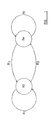
- FIGURE ONE is a state machine of a device embodying in the present invention
- FIGURE TWO is a circuit diagram for a control module embodying the present invention.
- a state machine for a device embodying the present invention is shown.
- the state machine has two operating states, a first state S0 and a second state Sn.
- the device is operable to receive an input comprising one of R1, a request that the system be in the first state S0 and R2, that the system be in the second state Sn.
- R1 a request that the system be in the first state S0 and R2
- R2 a request that the system be in the second state Sn.
- the device is a computer, although it might be suitable for any appropriate device.
- the first, S0 state may correspond to the G0 working condition of the computer and the state Sn may correspond to any one of states S1 to S4 representing sleeping states of the computer or S5 corresponding to the soft off state.
- a computer embodying the present invention may be responsive to a user's input to undergo a transition between a working state and a sleeping state or remain in the current working state or sleeping state as appropriate.
- control module embodying the invention may be provided as an ASIC or as a discrete module or embedded in an appropriate controller such as a Super I/O controller.
- a control module embodying the present invention is illustrated in Figure 2, by way of example.
- a control module embodying the present invention for a computer is generally illustrated at 20.
- the module comprises a first input, I 1 which is high when the device is in a first, power on state and low when in a second, power off, sleeping state, and a second input I 2 corresponding a requested state received from, in this example, a manually operable power switch generally illustrated at 25.
- the control module 20 generates an output O which in this example remains high and undergoes a transition from high to low to instruct a suitable power controller, here illustrated at 26, to cause a transition between the current state and requested state.
- the module 20 comprises a first filter element 21, a second filter element 22 and a third filter element 23.
- the second filter element 22 and third filter element 23 are each operable to generate a respective output instruction which is received by an output module 24, which generates the output O.
- the control module 20 operates as follows. When no input is received at the second input I 2 , point A on the circuit is held high by virtue of the connection via resistors R1, R2 to a standby power supply Vs, which remains high even when the computer is in a power off state. When a user operates the power switch 26 to generate a request, the input I 2 goes low and is held low as long as the user operates the power switch 26, for example holds down a power button. To request that the computer is in a first, power on state, the user operates the power switch 26, for a relatively short period of time and to request a second, power off state operates the power switch 26 for a relatively long period of time. The time period corresponding to each state can be set by selecting the resistance and capacitance values of resistors R 2 , R 3 , R 4 and capacitors C 2 , C 3 , C 4 .
- each filter element 21, 22, 23 are such that R2 and C2 have a time constant of two seconds, R3 and C3 have a time constants of one second and R4 and C4 have a time constant of 1.5 seconds.
- a input request signal having a length less than two seconds corresponds to a request for the computer to be in a first power on state whilst an input comprising a request signal having a length greater than two seconds corresponding to a request that the machine be in a second, power off state.
- the circuit operates as follows:
- filter element In filter element the high input I 1 is inverted by the NOT gate N1 and so a low signal is received by a PMOS Q1. Q1 is thus closed, and C2 is charged at voltage V s .
- the AND gate A1 of the output module 24 receives inputs G and H, and as input G goes low, output O will go low, subsequently going high as input G once again goes high.
- a suitable power controller for example a Super I/O controller, will respond to the high-low transition of output O and cause the computer to undergo a transition to the power off state.
- the second filter element 22 will generate an output comprising a 1 second pulse as discussed above, passed to input G of the second filter element 24.
- the output of the OR gate 02 will go low.
- input H will then go low as the request signal from A is transmitted by the R4C4 filter.
- the time constants R3C3 and R4C4 are selected such that input H goes low only after input G has gone low and then returned high.
- the output O of the AND gate A1 will go low in accordance with input G, go high and then go low again in accordance with input H.
- the power controller 26 will then receive two successive pulses, the first pulse turning the computer on for 0.5 seconds and the second pulse turning the computer off again. Thus, a short request signal will turn the computer on, whilst a long request signal will result in the computer remaining in the off condition.
- the present invention could be implemented as part of a power controller, for example a Super I/O controller, or be implemented as part of an on/off control of the computer, as an ASIC or as a circuit comprising discrete components or in any other way as desired.
Landscapes
- Engineering & Computer Science (AREA)
- Theoretical Computer Science (AREA)
- Physics & Mathematics (AREA)
- General Engineering & Computer Science (AREA)
- General Physics & Mathematics (AREA)
- Power Sources (AREA)
Abstract
Description
- This invention relates to a control module and a computer provided with a control module.
- Conventionally computers and other devices are provided with a manually operable power button which a user is able to operate to turn the computer or other device on or off. In many current devices, the power button does not act directly on the power supply, but instead generates a request to an appropriate power controller, for example, a Super I/O controller, to set the device to a power on or power off state. In some circumstances, it will not be immediately apparent whether a device is in a power on state or power off state causing a user to inadvertently turn the device on when it is desired that the device be turned off, or vice versa. This is particularly the case where the user of the computer or other device is visually impaired.
- An aim of the invention is to reduce or overcome the above problem.
- According to a first aspect of the invention we provide a control module for a device having a current state comprising one of a first state and a second state,
the control module being operable to receive a first input corresponding to the current state and a second input corresponding to a requested state,
the control module being operable when the current state and the requested state are different, to generate a output to cause a transition from the current state to the requested state. - The second input may comprise a request signal having a length, wherein a request signal having a relatively short length may correspond to the first state and wherein a request signal having a relatively long length may correspond to the second state.
- The module may comprise a first filter element operable to block a request signal having a relatively short length when the system is in the first state.
- The module may comprise a second filter element operable to generate a first output signal on receipt of the request signal.
- The module may comprise a third filter element operable to generate a second output signal on receipt of a request signal having a relatively long length when a device is in the second state.
- The first output instruction may comprise a first pulse and the second output instruction may comprise a second pulse delayed relative to the first pulse.
- The control module may comprises an output module operable to receive the first output instruction the second output instruction and generate the output accordingly.
- The first state may comprise a power on state and the second state may comprise a power off state.
- According to a second aspect of the invention, we provide a computer comprising a control module according to the first aspect of the invention, a manually operable power switch operable to generate the second input and a power control module responsive to the output to cause a transition between the power on state and the power off state.
- The invention will now be described by way of example only with reference to the accompanying drawings, wherein;
FIGURE ONE is a state machine of a device embodying in the present invention, and
FIGURE TWO is a circuit diagram for a control module embodying the present invention. - Referring to Figure 1, a state machine for a device embodying the present invention is shown. The state machine has two operating states, a first state S0 and a second state Sn. The device is operable to receive an input comprising one of R1, a request that the system be in the first state S0 and R2, that the system be in the second state Sn. As will be apparent, when the requested state is different to the current state a transition between states occurs. When the requested state matches the current state, the device remains in the current state.
- It is envisaged that the device is a computer, although it might be suitable for any appropriate device. In Figure 1 in accordance with the Advanced Configuration and Power Interface specification (ACPI) the first, S0 state, may correspond to the G0 working condition of the computer and the state Sn may correspond to any one of states S1 to S4 representing sleeping states of the computer or S5 corresponding to the soft off state. Thus, a computer embodying the present invention may be responsive to a user's input to undergo a transition between a working state and a sleeping state or remain in the current working state or sleeping state as appropriate.
- It will be apparent that a suitable control module embodying the invention may be provided as an ASIC or as a discrete module or embedded in an appropriate controller such as a Super I/O controller. A control module embodying the present invention is illustrated in Figure 2, by way of example.
- A control module embodying the present invention for a computer is generally illustrated at 20. The module comprises a first input, I1 which is high when the device is in a first, power on state and low when in a second, power off, sleeping state, and a second input I2 corresponding a requested state received from, in this example, a manually operable power switch generally illustrated at 25. The
control module 20 generates an output O which in this example remains high and undergoes a transition from high to low to instruct a suitable power controller, here illustrated at 26, to cause a transition between the current state and requested state. Themodule 20 comprises afirst filter element 21, asecond filter element 22 and athird filter element 23. Thesecond filter element 22 andthird filter element 23 are each operable to generate a respective output instruction which is received by anoutput module 24, which generates the output O. - The
control module 20 operates as follows. When no input is received at the second input I2, point A on the circuit is held high by virtue of the connection via resistors R1, R2 to a standby power supply Vs, which remains high even when the computer is in a power off state. When a user operates thepower switch 26 to generate a request, the input I2 goes low and is held low as long as the user operates thepower switch 26, for example holds down a power button. To request that the computer is in a first, power on state, the user operates thepower switch 26, for a relatively short period of time and to request a second, power off state operates thepower switch 26 for a relatively long period of time. The time period corresponding to each state can be set by selecting the resistance and capacitance values of resistors R2, R3, R4 and capacitors C2, C3, C4. - In this example, the resistance and capacitance values in each
filter element - The circuit operates as follows:
- In filter element the high input I1 is inverted by the NOT gate N1 and so a low signal is received by a PMOS Q1. Q1 is thus closed, and C2 is charged at voltage Vs.
- Where a request signal having a length of less than 2 seconds is received at input I2, it will be filtered by the R2C2 filter of
filter element 21, and thus no request signal will be sent to thesecond filter element 22 on input B or thethird filter element 23 on input C. There will thus be no change at the output O and there will be no transition in the state of the computer. - When a request signal longer than two seconds, i.e. longer than the R2C2 time constant of the first filter is received, A will go low and hence input sB and C will go low. In the
second filter element 22, the input E to OR gate will likewise go low. The output of NOT gate N2 will meanwhile go high, but input F to OR gate O1 will remain low for a time period dependent on the time constant R3C3. Both inputs E and F at OR gate O1 will therefore be low and input G of theoutput module 24 will go low. After a time period dependent on the time constant R3C3 input F will go high and input G will likewise go high. Because input I1 is high, the output ofOR gate 02 will remain high and thus input H will remain high. The AND gate A1 of theoutput module 24 receives inputs G and H, and as input G goes low, output O will go low, subsequently going high as input G once again goes high. A suitable power controller, for example a Super I/O controller, will respond to the high-low transition of output O and cause the computer to undergo a transition to the power off state. - As I, is low, the output of NOT gate N1 is high and so the PMOS Q1 will be open. Any input received at I2 will thus be passed to inputs B and C without filtering or delay.
- When a pulse of less than 2 seconds is received, at I2, inputs B and C will go low immediately, since there is no filtering effect from the
first filter element 21. As above, thesecond filter element 22 will generate an output passes to input G which goes low for a time period set by the time constant R3C3, in the present example 1 second, and then goes high. As the input I1 is low and the input C goes low, the output ofOR gate 02 will similarly go low. The time constant R4C4 is however selected such that a relatively short pulse will not be passed to the input H of the AND gate A1. Thus, input H remains high, whilst input G goes low for 1 second then returns high. The output O will then go low for 1 second and return high again, generating a pulse which thepower controller 26 recognises as an instruction to cause the computer to undergo a transition to the power on state. - If a pulse longer than 2 seconds is received at I2, then the
second filter element 22 will generate an output comprising a 1 second pulse as discussed above, passed to input G of thesecond filter element 24. As before, the output of theOR gate 02 will go low. Providing the request signal is longer than the time constant R4C4, input H will then go low as the request signal from A is transmitted by the R4C4 filter. The time constants R3C3 and R4C4 are selected such that input H goes low only after input G has gone low and then returned high. The output O of the AND gate A1 will go low in accordance with input G, go high and then go low again in accordance with input H. Thepower controller 26 will then receive two successive pulses, the first pulse turning the computer on for 0.5 seconds and the second pulse turning the computer off again. Thus, a short request signal will turn the computer on, whilst a long request signal will result in the computer remaining in the off condition. - It could be envisaged that the present invention could be implemented as part of a power controller, for example a Super I/O controller, or be implemented as part of an on/off control of the computer, as an ASIC or as a circuit comprising discrete components or in any other way as desired.
- In the present specification "comprises" means "includes or consists of" and "comprising" means "including or consisting of'.
- The features disclosed in the foregoing description, or the following claims, or the accompanying drawings, expressed in their specific forms or in terms of a means for performing the disclosed function, or a method or process for attaining the disclosed result, as appropriate, may, separately, or in any combination of such features, be utilised for realising the invention in diverse forms thereof.
Claims (9)
- A control module for a device having a current state comprising one of a first state and a second state,
the control module being operable to receive a first input corresponding to the current state and a second input corresponding to a requested state,
the control module being operable when the current state and the requested state are different, to generate a output to cause a transition from the current state to the requested state. - A control module according to claim 1 wherein the second input comprises a request signal having a length, wherein a request signal having a relatively short length corresponds to the first state and wherein a request signal having a relatively long length corresponds to the second state.
- A control module according to claim 2 wherein the module comprises a first filter element operable to block a request signal having a relatively short length when the system is in the first state.
- A control module according to claim 3 wherein the module comprises a second filter element operable to generate a first output signal on receipt of the request signal.
- A control module according to claim 4 wherein the module comprises a third filter element operable to generate a second output signal on receipt of a request signal having a relatively long length when a device is in the second state.
- A control module according to claim 5 wherein the first output instruction comprises a first pulse and the second output instruction comprises a second pulse delayed relative to the first pulse.
- A control module according to claim 5 or claim 6 wherein the control module comprises an output module operable to receive the first output instruction and the second output instruction and generate the output accordingly.
- A control module according to any one of the preceding claims wherein the first state comprises a power on state and the second state comprises a power off state.
- A computer comprising a control module according to claim 8, a manually operable power switch operable to generate the second input and a power control module responsive to the output to cause a transition between the power on state and the power off state.
Priority Applications (2)
| Application Number | Priority Date | Filing Date | Title |
|---|---|---|---|
| EP01410116A EP1293880A1 (en) | 2001-09-14 | 2001-09-14 | Control module |
| US10/242,289 US7065660B2 (en) | 2001-09-14 | 2002-09-12 | Power management based on current state and duration of a request signal |
Applications Claiming Priority (1)
| Application Number | Priority Date | Filing Date | Title |
|---|---|---|---|
| EP01410116A EP1293880A1 (en) | 2001-09-14 | 2001-09-14 | Control module |
Publications (1)
| Publication Number | Publication Date |
|---|---|
| EP1293880A1 true EP1293880A1 (en) | 2003-03-19 |
Family
ID=8183118
Family Applications (1)
| Application Number | Title | Priority Date | Filing Date |
|---|---|---|---|
| EP01410116A Withdrawn EP1293880A1 (en) | 2001-09-14 | 2001-09-14 | Control module |
Country Status (2)
| Country | Link |
|---|---|
| US (1) | US7065660B2 (en) |
| EP (1) | EP1293880A1 (en) |
Families Citing this family (4)
| Publication number | Priority date | Publication date | Assignee | Title |
|---|---|---|---|---|
| US8359646B2 (en) * | 2007-07-12 | 2013-01-22 | International Business Machines Corporation | Ensuring security of connection between thin client and client blade |
| TWI420287B (en) * | 2010-03-05 | 2013-12-21 | Wistron Corp | Power control system, power control method, and computer system having the same |
| CN102193614A (en) * | 2010-03-10 | 2011-09-21 | 纬创资通股份有限公司 | Power control system, power control method and computer system thereof |
| JP2015038651A (en) * | 2011-01-26 | 2015-02-26 | 株式会社東芝 | Information processing apparatus and control method thereof |
Citations (5)
| Publication number | Priority date | Publication date | Assignee | Title |
|---|---|---|---|---|
| JPH03276321A (en) * | 1990-03-27 | 1991-12-06 | Sharp Corp | Power unit for electronic equipment |
| US5404578A (en) * | 1988-12-07 | 1995-04-04 | Kabushiki Kaisha Toshiba | Radio telephone in which an off operation of an operator-actuated power switch is inhibited during a talk mode |
| JPH09261858A (en) * | 1996-03-26 | 1997-10-03 | Nec Corp | Power on/off control of computer |
| US5780941A (en) * | 1994-06-03 | 1998-07-14 | Nokia Telecommunications Oy | Control circuit |
| US6255746B1 (en) * | 1998-03-30 | 2001-07-03 | Asahi Kogaku Kogyo | Switch operation processing apparatus and method |
Family Cites Families (8)
| Publication number | Priority date | Publication date | Assignee | Title |
|---|---|---|---|---|
| US4245184A (en) * | 1979-03-23 | 1981-01-13 | Westinghouse Electric Corp. | AC Solid-state circuit breaker |
| US5251208A (en) * | 1991-12-19 | 1993-10-05 | At&T Bell Laboratories | Digital signal processor synchronous network |
| US5528238A (en) * | 1993-11-24 | 1996-06-18 | Intel Corporation | Process, apparatus and system for decoding variable-length encoded signals |
| US6445882B1 (en) * | 1995-05-30 | 2002-09-03 | Nikon Corporation | Camera which compensates for motion by setting the time at which a movable member begins moving and which adjusts the movement of the movable member for motion originating in the camera |
| JP3843145B2 (en) * | 1995-12-25 | 2006-11-08 | 株式会社ルネサステクノロジ | Synchronous semiconductor memory device |
| EP0884684B1 (en) * | 1997-06-13 | 2004-10-27 | Alcatel | Multiple interrupt handling method and apparatus |
| US6194940B1 (en) * | 1999-09-27 | 2001-02-27 | Lucent Technologies Inc. | Automatic clock switching |
| US6823413B2 (en) * | 2001-06-08 | 2004-11-23 | Oki Electronic Industry Co., Ltd. | Interrupt signal processing apparatus |
-
2001
- 2001-09-14 EP EP01410116A patent/EP1293880A1/en not_active Withdrawn
-
2002
- 2002-09-12 US US10/242,289 patent/US7065660B2/en not_active Expired - Fee Related
Patent Citations (5)
| Publication number | Priority date | Publication date | Assignee | Title |
|---|---|---|---|---|
| US5404578A (en) * | 1988-12-07 | 1995-04-04 | Kabushiki Kaisha Toshiba | Radio telephone in which an off operation of an operator-actuated power switch is inhibited during a talk mode |
| JPH03276321A (en) * | 1990-03-27 | 1991-12-06 | Sharp Corp | Power unit for electronic equipment |
| US5780941A (en) * | 1994-06-03 | 1998-07-14 | Nokia Telecommunications Oy | Control circuit |
| JPH09261858A (en) * | 1996-03-26 | 1997-10-03 | Nec Corp | Power on/off control of computer |
| US6255746B1 (en) * | 1998-03-30 | 2001-07-03 | Asahi Kogaku Kogyo | Switch operation processing apparatus and method |
Non-Patent Citations (2)
| Title |
|---|
| PATENT ABSTRACTS OF JAPAN vol. 016, no. 100 (P - 1323) 11 March 1992 (1992-03-11) * |
| PATENT ABSTRACTS OF JAPAN vol. 1998, no. 02 30 January 1998 (1998-01-30) * |
Also Published As
| Publication number | Publication date |
|---|---|
| US7065660B2 (en) | 2006-06-20 |
| US20030074589A1 (en) | 2003-04-17 |
Similar Documents
| Publication | Publication Date | Title |
|---|---|---|
| US7562236B2 (en) | Power saving apparatus and method | |
| US8166331B2 (en) | Computer system and operating method thereof | |
| EP1293880A1 (en) | Control module | |
| JP2004531787A (en) | System for controlling or regulating | |
| JPS6044854B2 (en) | Signal transmission method | |
| US6509723B2 (en) | Constant voltage regulator, method of controlling the same, and electric device provided with the same | |
| JP6471619B2 (en) | Electronic equipment | |
| US10908664B2 (en) | POE power supply system | |
| CN108352993B (en) | Ethernet bus, control device and method for waking up the control device of the Ethernet bus | |
| CN212289727U (en) | Vehicle power-on and power-off control circuit | |
| WO2004057449A2 (en) | Power supply level monitoring and reset generation | |
| JP2002300769A (en) | Power supply | |
| JP2000276267A (en) | Vehicle electronic control unit | |
| JPH0491534A (en) | Current consumption controlling device | |
| JPH0797721B2 (en) | Automotive antenna controller | |
| US20050202798A1 (en) | Method and circuit arrangement for switching an electronic circuit into a power-saving mode | |
| CN216052705U (en) | Power supply control equipment | |
| JPH01110022A (en) | Power equipment | |
| JP7505446B2 (en) | Power supply control device and power supply control method | |
| JP5782740B2 (en) | Semiconductor device for switching power supply control | |
| JP2001236129A (en) | Dc power unit and control method of the unit | |
| JP3367254B2 (en) | Power supply for power supply system | |
| JPH04361247A (en) | Cameras, communication devices and camera systems activated by external activation signals | |
| JPS6229987Y2 (en) | ||
| JP2546812Y2 (en) | Power supply circuit |
Legal Events
| Date | Code | Title | Description |
|---|---|---|---|
| PUAI | Public reference made under article 153(3) epc to a published international application that has entered the european phase |
Free format text: ORIGINAL CODE: 0009012 |
|
| AK | Designated contracting states |
Kind code of ref document: A1 Designated state(s): AT BE CH CY DE DK ES FI FR GB GR IE IT LI LU MC NL PT SE TR Designated state(s): AT BE CH CY DE DK ES FI FR GB GR IE IT LI LU MC NL PT SE TR |
|
| AX | Request for extension of the european patent |
Extension state: AL LT LV MK RO SI |
|
| AKX | Designation fees paid | ||
| 17P | Request for examination filed |
Effective date: 20030915 |
|
| RBV | Designated contracting states (corrected) |
Designated state(s): DE FR GB |
|
| REG | Reference to a national code |
Ref country code: DE Ref legal event code: 8566 |
|
| 17Q | First examination report despatched |
Effective date: 20040824 |
|
| STAA | Information on the status of an ep patent application or granted ep patent |
Free format text: STATUS: THE APPLICATION IS DEEMED TO BE WITHDRAWN |
|
| 18D | Application deemed to be withdrawn |
Effective date: 20071228 |