EP1291966A1 - Planar antenna for beam scanning - Google Patents
Planar antenna for beam scanning Download PDFInfo
- Publication number
- EP1291966A1 EP1291966A1 EP00917347A EP00917347A EP1291966A1 EP 1291966 A1 EP1291966 A1 EP 1291966A1 EP 00917347 A EP00917347 A EP 00917347A EP 00917347 A EP00917347 A EP 00917347A EP 1291966 A1 EP1291966 A1 EP 1291966A1
- Authority
- EP
- European Patent Office
- Prior art keywords
- dielectric
- grounding conductor
- rotman lens
- substrate
- connecting portion
- Prior art date
- Legal status (The legal status is an assumption and is not a legal conclusion. Google has not performed a legal analysis and makes no representation as to the accuracy of the status listed.)
- Granted
Links
Images


Classifications
-
- H—ELECTRICITY
- H01—ELECTRIC ELEMENTS
- H01Q—ANTENNAS, i.e. RADIO AERIALS
- H01Q13/00—Waveguide horns or mouths; Slot antennas; Leaky-waveguide antennas; Equivalent structures causing radiation along the transmission path of a guided wave
-
- H—ELECTRICITY
- H01—ELECTRIC ELEMENTS
- H01Q—ANTENNAS, i.e. RADIO AERIALS
- H01Q13/00—Waveguide horns or mouths; Slot antennas; Leaky-waveguide antennas; Equivalent structures causing radiation along the transmission path of a guided wave
- H01Q13/10—Resonant slot antennas
-
- H—ELECTRICITY
- H01—ELECTRIC ELEMENTS
- H01Q—ANTENNAS, i.e. RADIO AERIALS
- H01Q15/00—Devices for reflection, refraction, diffraction or polarisation of waves radiated from an antenna, e.g. quasi-optical devices
- H01Q15/02—Refracting or diffracting devices, e.g. lens, prism
- H01Q15/08—Refracting or diffracting devices, e.g. lens, prism formed of solid dielectric material
-
- H—ELECTRICITY
- H01—ELECTRIC ELEMENTS
- H01Q—ANTENNAS, i.e. RADIO AERIALS
- H01Q21/00—Antenna arrays or systems
- H01Q21/0006—Particular feeding systems
- H01Q21/0031—Parallel-plate fed arrays; Lens-fed arrays
-
- H—ELECTRICITY
- H01—ELECTRIC ELEMENTS
- H01Q—ANTENNAS, i.e. RADIO AERIALS
- H01Q21/00—Antenna arrays or systems
- H01Q21/0087—Apparatus or processes specially adapted for manufacturing antenna arrays
-
- H—ELECTRICITY
- H01—ELECTRIC ELEMENTS
- H01Q—ANTENNAS, i.e. RADIO AERIALS
- H01Q21/00—Antenna arrays or systems
- H01Q21/06—Arrays of individually energised antenna units similarly polarised and spaced apart
- H01Q21/061—Two dimensional planar arrays
- H01Q21/064—Two dimensional planar arrays using horn or slot aerials
-
- H—ELECTRICITY
- H01—ELECTRIC ELEMENTS
- H01Q—ANTENNAS, i.e. RADIO AERIALS
- H01Q25/00—Antennas or antenna systems providing at least two radiating patterns
- H01Q25/007—Antennas or antenna systems providing at least two radiating patterns using two or more primary active elements in the focal region of a focusing device
- H01Q25/008—Antennas or antenna systems providing at least two radiating patterns using two or more primary active elements in the focal region of a focusing device lens fed multibeam arrays
-
- H—ELECTRICITY
- H01—ELECTRIC ELEMENTS
- H01Q—ANTENNAS, i.e. RADIO AERIALS
- H01Q3/00—Arrangements for changing or varying the orientation or the shape of the directional pattern of the waves radiated from an antenna or antenna system
- H01Q3/44—Arrangements for changing or varying the orientation or the shape of the directional pattern of the waves radiated from an antenna or antenna system varying the electric or magnetic characteristics of reflecting, refracting, or diffracting devices associated with the radiating element
Definitions
- the present invention relates to a beam scanning plane antenna used for performing transmission/ reception in micro wave band or millimetric wave band.
- the beam scanning antenna which irradiates with electric waves in all directions of a specific range by changing the angle of the irradiation direction with time passage, often uses Rotman lens as a lens for converting signals from its system to scanning electric waves.
- this Rotman lens has a micro strip structure comprising a power feeding substrate 6 on which connecting lines 10 for connecting with the system, and power feeding lines 4 are formed; and a grounding conductor 3 attached on the rear face thereof.
- the power feeding lines 4 are connected to irradiating elements 5 through coaxial lines 15 connected to connectors.
- the number of the coaxial lines 15 increases depending on the number of the irradiating elements 5 and soldering is needed to connect the irradiating elements 5 with the coaxial lines 15.
- the number of assembly steps is large and it is difficult to form a thin structure because of its stereo structure.
- the antenna shown in Fig.1B uses electromagnetic coupling for connecting the connecting lines 16 extending from the Rotman lens pattern 8 with the irradiating elements 5.
- the connecting line 16 is prolonged, so that reduction in the size of the power feeding substrate 6 becomes difficult to achieve and further, loss on the connecting line increases.
- An object of the present invention is to provide a small beam scanning plane antenna which is excellent in terms of its thin structure and simplification of its assembly process.
- the beam scanning plane antenna described in claim 1 of the scope of claims for a patent is a beam scanning plane antenna formed by stacking a system connecting portion, a Rotman lens portion, and a beam scanning antenna portion in that order, the beam scanning antenna portion including: a power feeding substrate containing a plurality of antenna groups each constituted of an irradiating element, a power feeding line connected to the irradiating element and a first connecting portion connected electromagnetically to the Rotman lens portion; a first grounding conductor having a first slot at a position corresponding to the position of the irradiating element; a second grounding conductor having a second slot at a position corresponding to the position of the first connecting portion; a first dielectric provided between the first grounding conductor and the power feeding substrate; and a second dielectric provided between the power feeding substrate and the second grounding conductor, the Rotman lens portion including: a Rotman lens substrate having a Rotman lens pattern , a second connecting portion, which is connected to the Rotman lens pattern
- the system connecting portion comprises: a connecting substrate including a fourth connecting portion provided at a position corresponding to the position of the third connecting portion on the Rotman lens substrate and a connecting line for connecting at least the fourth connecting portion with the system; a fourth grounding conductor provided at least at a position corresponding to the position of the fourth connecting portion; a fifth dielectric provided between the third grounding conductor and the connecting substrate; and a sixth dielectric provided between the connecting substrate and the fourth grounding conductor, wherein the fifth dielectric, the connecting substrate, the sixth dielectric and the fourth grounding conductor are stacked in order.
- the beam scanning plane antenna according to claim 2 wherein a plurality of antenna groups on the power feeding substrate, the Rotman lens pattern on the Rotman lens substrate, the second connecting portions, the third connecting portion, the fourth connecting portions and the connecting lines are formed by removing unnecessary copper foil by etching from copper coated lamination film in which copper foil is bonded to polyimide film as a foundation material.
- the beam scanning plane antenna according to claim 2 wherein a foamed body having a relative dielectric constant of 1.1 is used for the first dielectric, the second dielectric, the third dielectric, the fourth dielectric, the fifth dielectric and the sixth dielectric.
- the beam scanning plane antenna according to claim 1 wherein the first slot is a square whose one side is 0.59 times longer than free space wavelength ⁇ 0 ⁇
- the beam scanning plane antenna according to claim 2 wherein an aluminum plate is used for the first grounding conductor, the second grounding conductor, the third grounding conductor and the fourth grounding conductor.
- a plurality of antenna groups are formed on a power feeding substrate 61 by removing unnecessary copper foil by etching from a copper coated lamination film in which copper foil is attached on a polyimide film as its foundation material thereof.
- Each antenna group comprises an irradiating element 50, a power feeding line 40 connected thereto and a first connecting portion 51 connected electromagnetically to a Rotman lens portion 103.
- the copper coated lamination film it is permissible to use a flexible substrate in which aluminum foil is bonded to a polyethylene terephthalate film.
- a ROTOAMAN lens substrate 62 and a connecting substrate 63 can be produced.
- any metallic plate or any plated plastic plate may be used.
- the aluminum plate is used, preferably it can be manufactured with light weight and at a cheap price.
- a second grounding conductor 12, a third grounding conductor 13, and a fourth grounding conductor 14 may be manufactured in the same manner.
- a first dielectric 31 As a first dielectric 31, a second dielectric 32, a third dielectric 33, a fourth dielectric 34, a fifth dielectric 35 and a sixth dielectric 36, preferably, air or a foamed body having a low relative dielectric constant is used.
- the beam scanning plane antenna is formed by stacking a beam scan antenna portion 102, a Rotman lens portion 103 and a system connecting portion 104 in order from top.
- the beam scanning antenna portion 102 is formed by stacking the first grounding conductor 11, the first dielectric 31, the power feeding substrate 61, the second dielectric 32 and the second grounding conductor 12 in order from top.
- a plurality of antenna groups are formed on the power feeding substrate 61 by removing unnecessary copper foil from copper coated lamination film in which copper foil having the thickness of 35 ⁇ m is bonded on polyimide film having the thickness of 25 ⁇ m as its foundation material.
- Each antenna group is constituted of an irradiating element 50, a power feeding line 40 connected thereto and a first connecting portion 51 connected electromagnetically to the Rotman lens portion 103.
- First slots 2 each is a square whose one side is 0.59 times longer than free space wavelength ⁇ 0 are provided at positions of the first grounding conductor 11 corresponding to the positions of irradiating elements 50. The interval for the arrangement of the first slots 2 is 0.90 times longer than the free space wavelength ⁇ 0 .
- Second slots 71 are provided at positions of the second grounding conductor 12 corresponding to the positions of the first connecting portions 51.
- a foamed body 0.3 mm thick having a relative dielectric constant of 1.1 is used as the first dielectric 31 and the second dielectric 32.
- the Rotman lens portion 103 is formed by stacking the third dielectric 33, the Rotman lens substrate 62, the fourth dielectric 34, and the third grounding conductor 13 in order from top.
- a Rotman lens pattern 8, a second connecting portion 52 and a third connecting portion 92 are formed on the Rotman lens substrate 62 by removing unnecessary copper foil by etching from copper coated lamination film in which copper foil 35 ⁇ m thick is bonded on polyimide film 25 ⁇ m thick as its foundation material.
- the second connecting portion 52 is connected to the ROTOAMAN lens pattern 8 thereby connecting the ROROMAN lens pattern 8 with the first connecting portion 51.
- the third connecting portion 92 is connected to the Rotman lens pattern 8, thereby connecting the Rotman lens pattern 8 with the system connecting portion 104 electromagnetically.
- Third connecting conductor 13 an aluminum plate 3 mm thick is used as the third connecting conductor 13. Third slots 72 are provided at positions of the third grounding conductor 13 corresponding to the positions of the third connecting portions 92.
- a foamed body 0.3 mm thick having a relative dielectric constant of 1.1 is used as the third dielectric 33 and the fourth dielectric 34.
- the system connecting portion 104 is formed by stacking the fourth dielectric 35, the connecting substrate 63, the fifth dielectric 36 and the fourth grounding conductor 14 in order from top.
- the fourth connecting portions 91 and the connecting lines 101 are formed on the connecting substrate 63 by removing unnecessary copper foil by etching from copper coated lamination film in which copper foil 35 ⁇ m is bonded on polyimide film 25 ⁇ m thick as a foundation material.
- the fourth connecting portions 91 are provided at positions of the ROTOAMAN lens substrate 62 corresponding to the positions of the third connecting portions 92.
- the connecting lines 101 connect at least the fourth connecting portions 91 with the system.
- the fourth grounding conductor 14 is provided at least at a position corresponding to the fourth connecting portion 91.
- a foamed body 0.3 mm thick having a relative dielectric constant of 1.1 is used as the fifth dielectric 35 and the sixth dielectric 36.
- the beam scanning plane antenna according to the embodiment of the present invention is constructed as described above.
- this beam scanning plane antenna is formed by stacking the system connecting portion 104, the Rotman lens portion 103 and the beam scanning antenna portion 102 in order from bottom.
- this beam scanning plane antenna is formed by stacking the fourth grounding conductor 14, the sixth dielectric body 36, the connecting substrate 63, the fifth dielectric body 35, the third grounding conductor 13, the fourth dielectric body 34, the Rotman lens substrate 62, the third dielectric 33, the second grounding conductor 12, the second dielectric 32, the power feeding substrate 61, the first dielectric body 31 and the first grounding conductor 11 in order from bottom.
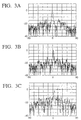
- Fig.3A shows the directivity characteristic when beam is projected in the perpendicular direction.
- Fig. 3B is a diagram showing the directivity characteristic when the beam is inclined two degrees from the perpendicular direction.
- Fig.3C is a diagram showing directivity characteristic when the beam is inclined four degrees from the perpendicular direction.
- the present invention is capable of providing a small beam scanning plane antenna which is excellent in terms of its thin structure and simplification of its assembly process.
Landscapes
- Engineering & Computer Science (AREA)
- Manufacturing & Machinery (AREA)
- Variable-Direction Aerials And Aerial Arrays (AREA)
- Aerials With Secondary Devices (AREA)
Abstract
Description
Claims (6)
- A beam scanning plane antenna formed by stacking a system connecting portion (104), a Rotman lens portion (103), and a beam scanning antenna portion (102) in that order,
the beam scanning antenna portion (102) including:the Rotman lens portion (103) including:a power feeding substrate (61) containing a plurality of antenna groups each constituted of an irradiating element (50), a power feeding line (40) connected to the irradiating element (50) and a first connecting portion (51) connected electromagnetically to the Rotman lens portion (103);a first grounding conductor (11) having a first slot (2) at a position corresponding to the position of the irradiating element (50);a second grounding conductor (12) having a second slot (71) at a position corresponding to the position of the first connecting portion (51);a first dielectric (31) provided between the first grounding conductor (11) and the power feeding substrate (61); anda second dielectric (32) provided between the power feeding substrate (61) and the second grounding conductor (12),wherein the Rotman lens portion (103) and the beam scanning antenna portion (102) are formed by stacking the third grounding conductor (13), the fourth dielectric (34), the Rotman lens substrate (62), the third dielectric (33), the second grounding conductor (12), the second dielectric (32), the power feeding substrate (61), the first dielectric (31) and the first grounding conductor (11) in that order.a Rotman lens substrate (62) having a Rotman lens pattern (8), a second connecting portion (52), which is connected to the Rotman lens pattern (8), for connecting the Rotman lens pattern (8) with the first connecting portion (51), and a third connecting portion (92), which is connected to the Rotman lens pattern (8), for connecting the Rotman lens pattern (8) with the system connecting portion (104) electromagnetically;a third grounding conductor (13) having a third slot (72) at a position corresponding to the position of the third connecting portion (92);a third dielectric (33) provided between the second grounding conductor (12) and the Rotman lens substrate (62); anda fourth dielectric (34) provided between the Rotman lens substrate (62) and the third connecting conductor (13), - The beam scanning plane antenna according to claim 1 wherein the system connecting portion (104) comprises:wherein the fifth dielectric (35), the connecting substrate (63), the sixth dielectric (36) and the fourth grounding conductor (14) are stacked in that order.a connecting substrate (63) including a fourth connecting portion (91) provided at a position corresponding to the position of the third connecting portion (92) on the Rotman lens substrate (62) and a connecting line (101) for connecting at least the fourth connecting portion (91) with the system;a fourth grounding conductor (14) provided at least at a position corresponding to the position of the fourth connecting portion (91);a fifth dielectric (35) provided between the third grounding conductor (13) and the connecting substrate (63); anda sixth dielectric (36) provided between the connecting substrate (63) and the fourth grounding conductor (14),
- The beam scanning plane antenna according to claim 2 wherein a plurality of antenna groups on the power feeding substrate (61), the Rotman lens pattern (8) on the Rotman lens substrate (62), the second connecting portions (52), the third connecting portion (92), the fourth connecting portions (91) and the connecting lines (101) are formed by removing unnecessary copper foil by etching from copper coated lamination film in which copper foil is bonded to polyimide film as a foundation material.
- The beam scanning plane antenna according to claim 2 wherein a foamed body having a relative dielectric constant of 1.1 is used for the first dielectric (31), the second dielectric (32), the third dielectric (33), the fourth dielectric (34), the fifth dielectric (35) and the sixth dielectric (36).
- The beam scanning plane antenna according to claim 1 wherein the first slot is a square whose one side is 0.59 times longer than free space wavelength λ0.
- The beam scanning plane antenna according to claim 2 wherein an aluminum plate is used for the first grounding conductor (11), the second grounding conductor (12), the third grounding conductor (13) and the fourth grounding conductor (14).
Priority Applications (1)
| Application Number | Priority Date | Filing Date | Title |
|---|---|---|---|
| EP10153822.1A EP2184805B1 (en) | 2000-04-18 | 2000-04-18 | Beam scanning plane antenna |
Applications Claiming Priority (1)
| Application Number | Priority Date | Filing Date | Title |
|---|---|---|---|
| PCT/JP2000/002528 WO2001080357A1 (en) | 2000-04-18 | 2000-04-18 | Planar antenna for beam scanning |
Related Child Applications (2)
| Application Number | Title | Priority Date | Filing Date |
|---|---|---|---|
| EP10153822.1A Division EP2184805B1 (en) | 2000-04-18 | 2000-04-18 | Beam scanning plane antenna |
| EP10153822.1 Division-Into | 2010-02-17 |
Publications (3)
| Publication Number | Publication Date |
|---|---|
| EP1291966A1 true EP1291966A1 (en) | 2003-03-12 |
| EP1291966A4 EP1291966A4 (en) | 2008-07-02 |
| EP1291966B1 EP1291966B1 (en) | 2010-08-11 |
Family
ID=11735932
Family Applications (2)
| Application Number | Title | Priority Date | Filing Date |
|---|---|---|---|
| EP00917347A Expired - Lifetime EP1291966B1 (en) | 2000-04-18 | 2000-04-18 | Planar antenna for beam scanning |
| EP10153822.1A Expired - Lifetime EP2184805B1 (en) | 2000-04-18 | 2000-04-18 | Beam scanning plane antenna |
Family Applications After (1)
| Application Number | Title | Priority Date | Filing Date |
|---|---|---|---|
| EP10153822.1A Expired - Lifetime EP2184805B1 (en) | 2000-04-18 | 2000-04-18 | Beam scanning plane antenna |
Country Status (5)
| Country | Link |
|---|---|
| US (1) | US6720931B1 (en) |
| EP (2) | EP1291966B1 (en) |
| KR (1) | KR100486831B1 (en) |
| DE (1) | DE60044826D1 (en) |
| WO (1) | WO2001080357A1 (en) |
Cited By (6)
| Publication number | Priority date | Publication date | Assignee | Title |
|---|---|---|---|---|
| WO2006029926A1 (en) * | 2004-09-13 | 2006-03-23 | Robert Bosch Gmbh | Monostatic planar multibeam radar sensor |
| US7301504B2 (en) | 2004-07-14 | 2007-11-27 | Ems Technologies, Inc. | Mechanical scanning feed assembly for a spherical lens antenna |
| EP2190066A3 (en) * | 2005-03-16 | 2010-06-09 | Hitachi Chemical Co., Ltd. | Planar antenna module, triple plate planar array antenna, and triple plate feeder - waveguide converter |
| US8203778B2 (en) | 2010-03-22 | 2012-06-19 | Samsung Electronics Co., Ltd. | Electrophoretic display device and method for manufacturing same |
| EP2372835A4 (en) * | 2008-11-28 | 2015-06-17 | Hitachi Chemical Co Ltd | MULTI-BEAM ANTENNA DEVICE |
| SE1951395A1 (en) * | 2019-12-04 | 2021-06-05 | Sencept Ab | A scanning antenna comprising several stacked microwave lenses |
Families Citing this family (13)
| Publication number | Priority date | Publication date | Assignee | Title |
|---|---|---|---|---|
| EP1371112B1 (en) * | 2001-03-21 | 2007-05-02 | Microface Co. Ltd | Waveguide slot antenna and manufacturing method thereof |
| US7728772B2 (en) * | 2006-06-09 | 2010-06-01 | The Regents Of The University Of Michigan | Phased array systems and phased array front-end devices |
| US7656345B2 (en) | 2006-06-13 | 2010-02-02 | Ball Aerospace & Technoloiges Corp. | Low-profile lens method and apparatus for mechanical steering of aperture antennas |
| US8604989B1 (en) | 2006-11-22 | 2013-12-10 | Randall B. Olsen | Steerable antenna |
| EP2393156B1 (en) | 2009-01-29 | 2014-12-03 | Hitachi Chemical Company, Ltd. | Multi-beam antenna apparatus |
| EP2523256B1 (en) | 2011-05-13 | 2013-07-24 | Thomson Licensing | Multibeam antenna system |
| US9160049B2 (en) | 2011-11-16 | 2015-10-13 | Commscope Technologies Llc | Antenna adapter |
| US8866687B2 (en) | 2011-11-16 | 2014-10-21 | Andrew Llc | Modular feed network |
| US8558746B2 (en) | 2011-11-16 | 2013-10-15 | Andrew Llc | Flat panel array antenna |
| KR101306784B1 (en) * | 2011-12-30 | 2013-09-10 | 연세대학교 산학협력단 | Rotman lens with asymmetrical sturcture and beam forming antenna by using thereof |
| CN112652889A (en) * | 2019-09-25 | 2021-04-13 | 天津大学 | Novel Rotman lens based on medium integrated suspension line |
| US11303252B2 (en) | 2019-09-25 | 2022-04-12 | Analog Devices International Unlimited Company | Breakdown protection circuit for power amplifier |
| CN116914438B (en) * | 2023-05-24 | 2024-05-31 | 广东福顺天际通信有限公司 | Deformable lens and antenna with deflectable beam direction |
Family Cites Families (10)
| Publication number | Priority date | Publication date | Assignee | Title |
|---|---|---|---|---|
| US3761936A (en) * | 1971-05-11 | 1973-09-25 | Raytheon Co | Multi-beam array antenna |
| US4408205A (en) * | 1981-06-25 | 1983-10-04 | International Telephone And Telegraph Corporation | Multiple beam antenna feed arrangement for generating an arbitrary number of independent steerable nulls |
| JPH02168703A (en) * | 1988-09-02 | 1990-06-28 | Toshiba Corp | Plane antenna and its production |
| US4899164A (en) * | 1988-09-16 | 1990-02-06 | The United States Of America As Represented By The Secretary Of The Air Force | Slot coupled microstrip constrained lens |
| US5278569A (en) * | 1990-07-25 | 1994-01-11 | Hitachi Chemical Company, Ltd. | Plane antenna with high gain and antenna efficiency |
| JPH0529832A (en) | 1991-07-24 | 1993-02-05 | Nec Corp | Plane antenna |
| JPH1127033A (en) | 1997-07-08 | 1999-01-29 | Hitachi Chem Co Ltd | Planar antenna |
| US6130653A (en) * | 1998-09-29 | 2000-10-10 | Raytheon Company | Compact stripline Rotman lens |
| JP4089043B2 (en) * | 1998-10-20 | 2008-05-21 | 日立化成工業株式会社 | Planar antenna for beam scanning |
| US6049311A (en) * | 1999-03-05 | 2000-04-11 | The Whitaker Corporation | Planar flat plate scanning antenna |
-
2000
- 2000-04-18 DE DE60044826T patent/DE60044826D1/en not_active Expired - Lifetime
- 2000-04-18 EP EP00917347A patent/EP1291966B1/en not_active Expired - Lifetime
- 2000-04-18 US US10/257,366 patent/US6720931B1/en not_active Expired - Lifetime
- 2000-04-18 WO PCT/JP2000/002528 patent/WO2001080357A1/en not_active Ceased
- 2000-04-18 KR KR10-2002-7013860A patent/KR100486831B1/en not_active Expired - Lifetime
- 2000-04-18 EP EP10153822.1A patent/EP2184805B1/en not_active Expired - Lifetime
Cited By (12)
| Publication number | Priority date | Publication date | Assignee | Title |
|---|---|---|---|---|
| US7301504B2 (en) | 2004-07-14 | 2007-11-27 | Ems Technologies, Inc. | Mechanical scanning feed assembly for a spherical lens antenna |
| WO2006029926A1 (en) * | 2004-09-13 | 2006-03-23 | Robert Bosch Gmbh | Monostatic planar multibeam radar sensor |
| US7786928B2 (en) | 2004-09-13 | 2010-08-31 | Robert Bosch Gmbh | Monostatic planar multi-beam radar sensor |
| EP2190066A3 (en) * | 2005-03-16 | 2010-06-09 | Hitachi Chemical Co., Ltd. | Planar antenna module, triple plate planar array antenna, and triple plate feeder - waveguide converter |
| US8253511B2 (en) | 2005-03-16 | 2012-08-28 | Hitachi Chemical Co., Ltd. | Triple plate feeder—waveguide converter having a square resonance patch pattern |
| EP1860731B1 (en) * | 2005-03-16 | 2014-12-17 | Hitachi Chemical Co., Ltd. | Planar antenna module, triplate planar array antenna, and triplate line-waveguide converter |
| EP2372835A4 (en) * | 2008-11-28 | 2015-06-17 | Hitachi Chemical Co Ltd | MULTI-BEAM ANTENNA DEVICE |
| US8203778B2 (en) | 2010-03-22 | 2012-06-19 | Samsung Electronics Co., Ltd. | Electrophoretic display device and method for manufacturing same |
| US8446662B2 (en) | 2010-03-22 | 2013-05-21 | Samsung Display Co., Ltd. | Electrophoretic display device and method for manufacturing same |
| SE1951395A1 (en) * | 2019-12-04 | 2021-06-05 | Sencept Ab | A scanning antenna comprising several stacked microwave lenses |
| WO2021110947A1 (en) * | 2019-12-04 | 2021-06-10 | Sencept Ab | Scanning antenna |
| SE543769C2 (en) * | 2019-12-04 | 2021-07-20 | Sencept Ab | A scanning antenna comprising several stacked microwave lenses |
Also Published As
| Publication number | Publication date |
|---|---|
| EP2184805A1 (en) | 2010-05-12 |
| DE60044826D1 (en) | 2010-09-23 |
| EP2184805B1 (en) | 2015-11-04 |
| KR100486831B1 (en) | 2005-04-29 |
| US6720931B1 (en) | 2004-04-13 |
| KR20020093048A (en) | 2002-12-12 |
| EP1291966A4 (en) | 2008-07-02 |
| EP1291966B1 (en) | 2010-08-11 |
| WO2001080357A1 (en) | 2001-10-25 |
Similar Documents
| Publication | Publication Date | Title |
|---|---|---|
| US6720931B1 (en) | Planar antenna for beam scanning | |
| US11742888B2 (en) | Systems and methods for signal communication with scalable, modular network nodes | |
| EP2393156B1 (en) | Multi-beam antenna apparatus | |
| US8698689B2 (en) | Multi-beam antenna device | |
| JP2001094340A (en) | Slot array antenna with cavity | |
| CN106450782A (en) | End-on-fire antenna and radar assembly | |
| CN113013606B (en) | Adjustable array antenna based on substrate integrated waveguide and terminal | |
| US20230238712A1 (en) | Antenna Apparatus, Method for Producing Antenna Apparatus, Radar, and Terminal | |
| JP4089043B2 (en) | Planar antenna for beam scanning | |
| US6967624B1 (en) | Wideband antenna element and array thereof | |
| KR20200040403A (en) | Inverted Feeding Microstrip Ppatch Aantenna for vehicle radar | |
| US20040113856A1 (en) | Antenna | |
| JP2012249004A (en) | Wide angle directional antenna | |
| JP4227589B2 (en) | Active array antenna | |
| JPH06125214A (en) | Planar antenna | |
| JPH04154303A (en) | Triplet type plane antenna | |
| JPS63128803A (en) | Structure of microstrip antenna |
Legal Events
| Date | Code | Title | Description |
|---|---|---|---|
| PUAI | Public reference made under article 153(3) epc to a published international application that has entered the european phase |
Free format text: ORIGINAL CODE: 0009012 |
|
| 17P | Request for examination filed |
Effective date: 20021106 |
|
| AK | Designated contracting states |
Kind code of ref document: A1 Designated state(s): DE FR GB |
|
| A4 | Supplementary search report drawn up and despatched |
Effective date: 20080529 |
|
| 17Q | First examination report despatched |
Effective date: 20080908 |
|
| GRAP | Despatch of communication of intention to grant a patent |
Free format text: ORIGINAL CODE: EPIDOSNIGR1 |
|
| GRAS | Grant fee paid |
Free format text: ORIGINAL CODE: EPIDOSNIGR3 |
|
| GRAA | (expected) grant |
Free format text: ORIGINAL CODE: 0009210 |
|
| AK | Designated contracting states |
Kind code of ref document: B1 Designated state(s): DE FR GB |
|
| REG | Reference to a national code |
Ref country code: GB Ref legal event code: FG4D |
|
| REF | Corresponds to: |
Ref document number: 60044826 Country of ref document: DE Date of ref document: 20100923 Kind code of ref document: P |
|
| PLBE | No opposition filed within time limit |
Free format text: ORIGINAL CODE: 0009261 |
|
| STAA | Information on the status of an ep patent application or granted ep patent |
Free format text: STATUS: NO OPPOSITION FILED WITHIN TIME LIMIT |
|
| 26N | No opposition filed |
Effective date: 20110512 |
|
| REG | Reference to a national code |
Ref country code: DE Ref legal event code: R097 Ref document number: 60044826 Country of ref document: DE Effective date: 20110512 |
|
| REG | Reference to a national code |
Ref country code: FR Ref legal event code: PLFP Year of fee payment: 17 |
|
| REG | Reference to a national code |
Ref country code: FR Ref legal event code: PLFP Year of fee payment: 18 |
|
| REG | Reference to a national code |
Ref country code: FR Ref legal event code: PLFP Year of fee payment: 19 |
|
| PGFP | Annual fee paid to national office [announced via postgrant information from national office to epo] |
Ref country code: DE Payment date: 20190418 Year of fee payment: 20 |
|
| PGFP | Annual fee paid to national office [announced via postgrant information from national office to epo] |
Ref country code: FR Payment date: 20190424 Year of fee payment: 20 |
|
| REG | Reference to a national code |
Ref country code: DE Ref legal event code: R082 Ref document number: 60044826 Country of ref document: DE Representative=s name: HOFFMANN - EITLE PATENT- UND RECHTSANWAELTE PA, DE Ref country code: DE Ref legal event code: R081 Ref document number: 60044826 Country of ref document: DE Owner name: HITACHI KOKUSAI ELECTRIC INC., TOKYO, JP Free format text: FORMER OWNER: HITACHI CHEMICAL CO., LTD., TOKYO, JP |
|
| PGFP | Annual fee paid to national office [announced via postgrant information from national office to epo] |
Ref country code: GB Payment date: 20190418 Year of fee payment: 20 |
|
| REG | Reference to a national code |
Ref country code: GB Ref legal event code: 732E Free format text: REGISTERED BETWEEN 20191031 AND 20191106 |
|
| REG | Reference to a national code |
Ref country code: DE Ref legal event code: R071 Ref document number: 60044826 Country of ref document: DE |
|
| REG | Reference to a national code |
Ref country code: GB Ref legal event code: PE20 Expiry date: 20200417 |
|
| PG25 | Lapsed in a contracting state [announced via postgrant information from national office to epo] |
Ref country code: GB Free format text: LAPSE BECAUSE OF EXPIRATION OF PROTECTION Effective date: 20200417 |