EP1291959A1 - Directional coupler - Google Patents
Directional coupler Download PDFInfo
- Publication number
- EP1291959A1 EP1291959A1 EP01983269A EP01983269A EP1291959A1 EP 1291959 A1 EP1291959 A1 EP 1291959A1 EP 01983269 A EP01983269 A EP 01983269A EP 01983269 A EP01983269 A EP 01983269A EP 1291959 A1 EP1291959 A1 EP 1291959A1
- Authority
- EP
- European Patent Office
- Prior art keywords
- line
- dielectric substrate
- directional coupler
- formation surface
- strip conductor
- Prior art date
- Legal status (The legal status is an assumption and is not a legal conclusion. Google has not performed a legal analysis and makes no representation as to the accuracy of the status listed.)
- Withdrawn
Links
Images





Classifications
-
- H—ELECTRICITY
- H01—ELECTRIC ELEMENTS
- H01P—WAVEGUIDES; RESONATORS, LINES, OR OTHER DEVICES OF THE WAVEGUIDE TYPE
- H01P5/00—Coupling devices of the waveguide type
- H01P5/12—Coupling devices having more than two ports
- H01P5/16—Conjugate devices, i.e. devices having at least one port decoupled from one other port
- H01P5/18—Conjugate devices, i.e. devices having at least one port decoupled from one other port consisting of two coupled guides, e.g. directional couplers
-
- H—ELECTRICITY
- H01—ELECTRIC ELEMENTS
- H01P—WAVEGUIDES; RESONATORS, LINES, OR OTHER DEVICES OF THE WAVEGUIDE TYPE
- H01P5/00—Coupling devices of the waveguide type
- H01P5/12—Coupling devices having more than two ports
- H01P5/16—Conjugate devices, i.e. devices having at least one port decoupled from one other port
- H01P5/18—Conjugate devices, i.e. devices having at least one port decoupled from one other port consisting of two coupled guides, e.g. directional couplers
- H01P5/184—Conjugate devices, i.e. devices having at least one port decoupled from one other port consisting of two coupled guides, e.g. directional couplers the guides being strip lines or microstrips
- H01P5/185—Edge coupled lines
-
- H—ELECTRICITY
- H01—ELECTRIC ELEMENTS
- H01P—WAVEGUIDES; RESONATORS, LINES, OR OTHER DEVICES OF THE WAVEGUIDE TYPE
- H01P5/00—Coupling devices of the waveguide type
- H01P5/12—Coupling devices having more than two ports
- H01P5/16—Conjugate devices, i.e. devices having at least one port decoupled from one other port
- H01P5/18—Conjugate devices, i.e. devices having at least one port decoupled from one other port consisting of two coupled guides, e.g. directional couplers
- H01P5/184—Conjugate devices, i.e. devices having at least one port decoupled from one other port consisting of two coupled guides, e.g. directional couplers the guides being strip lines or microstrips
- H01P5/187—Broadside coupled lines
Definitions
- the present invention relates to a directional coupler for coupling a high frequency signal, which is inputted into a primary line, to a subsidiary line by means of electromagnetic coupling of the primary line and the subsidiary line, which are formed on a dielectric substrate.
- Fig. 1 is a diagram illustrating a configuration of a conventional directional coupler, which was disclosed in JP-B No. 03-73164 for example.
- Fig. 2 is a diagram illustrating a cross section of the directional coupler taken along a line A-A' shown in Fig. 1.
- a reference numeral 101 is a dielectric substrate having two formation surfaces; reference numerals 102 and 103 are a first inner conductor and a second inner conductor respectively; reference numerals 102a, 102b, 103a, and 103b are strip conductor patterns; a reference numeral 104 represents outer conductors; reference numerals 105a and 105b are input/output terminals of the first inner conductor 102; reference numerals 105c and 105d are input/output terminals of the second inner conductor 103; and a reference numeral 106 is a coupled line.
- a pair of the strip conductor patterns 102a and 102b is kept in the same potential and constitutes the first inner conductor 102.
- a pair of the strip conductor patterns 103a and 103b is kept in the same potential and constitutes the second inner conductor 103.
- the strip conductor patterns 102a and 102b are formed on both formation surfaces of the dielectric substrate 101 so that they sandwich the dielectric substrate 101.
- the strip conductor patterns 103a and 103b are also formed on both formation surfaces of the dielectric substrate 101 so that they sandwich the dielectric substrate 101.
- the first inner conductor 102 and the second inner conductor 103 are adjacent to each other so as to be coupled electromagnetically in the coupled line 106.
- a length of the coupled line 106 is about 1/4 of a wavelength at a desired frequency.
- outer conductors 104 are placed in parallel at a predetermined distance so as to sandwich the first inner conductor 102, the second inner conductor 103, and the dielectric substrate 101.
- the high frequency signal When a high frequency signal is inputted from the input/output terminal 105a of the directional coupler, the high frequency signal propagates through the first inner conductor 102, and then couples electromagnetically to the second inner conductor 103 in the coupled line 106.
- a length of the coupled line 106 is 1/4 of a wavelength in an even mode (a mode for a case in which two electromagnetically coupled lines are excited at in-phase equal amplitude) and in an odd mode (a mode for a case in which two electromagnetically coupled lines are excited at out-of-phase equal amplitude)
- a coupled high frequency signal has directivity. Therefore, the coupled high frequency signal does not appear in the input/output terminal 105d, but is taken from the input/output terminal 105c.
- the conventional directional coupler is configured as described above, there is the following problem: a wavelength shortening rate in the even mode is different from that in the odd mode, which causes difference in phase velocity between the modes, resulting in characteristic degradation of the directional coupler.
- Fig. 3 illustrates electric field distribution of the directional coupler shown in Fig. 2; and Figs. 3(a) and 3(b) are a diagram in the even mode and a diagram in the odd mode respectively. Arrows in the diagrams represent electric fields.
- the present invention has been made in order to solve the problem described above, and aims to configure a directional coupler that achieves good directivity and reflection characteristics by compensating for the difference in phase velocity between the even mode and the odd mode, which is caused by difference in the wavelength shortening rate.
- a directional coupler is configured to have a reactive element that is mounted on a primary line and a subsidiary line, and that compensates for a reactive component equivalently possessed by a coupled line.
- a directional coupler is configured to have a capacitive element that is mounted on a primary line and a subsidiary line, and that compensates for a parallel capacitive component equivalently possessed by the coupled line.
- a directional coupler is configured to use a capacitor, which is connected from a position between the input/output terminal and the coupled line to the ground, as a capacitive element.
- a directional coupler according to the present invention is configured to use an open stub, which is mounted between the input/output terminal and the coupled line, as a capacitive element.
- a directional coupler according to the present invention is configured to use a low impedance line, which is provided between the input/output terminal and the coupled line, as a capacitive element.
- a directional coupler is so devised that the primary line and the subsidiary line have an intersection area where propagating directions of a high frequency signal intersect at the center of the coupled line when projecting the primary line and the subsidiary line from a normal line direction of the formation surface to a plane parallel to the above-mentioned formation surface.
- a directional coupler is so devised that the primary line and the subsidiary line have an intersection area where propagating directions of a high frequency signal intersect at the center of the coupled line when projecting the primary line and the subsidiary line from a normal line direction of the formation surface to a plane parallel to the above-mentioned formation surface.
- a directional coupler is so devised that the primary line and the subsidiary line have an intersection area where propagating directions of a high frequency signal intersect at the center of the coupled line when projecting the primary line and the subsidiary line from a normal line direction of the formation surface to a plane parallel to the above-mentioned formation surface.
- a directional coupler is so devised that the primary line and the subsidiary line have an intersection area where propagating directions of a high frequency signal intersect at the center of the coupled line when projecting the primary line and the subsidiary line from a normal line direction of the formation surface to a plane parallel to the above-mentioned formation surface.
- a directional coupler is devised in the following manner: a primary line is provided by the first strip conductor pattern that is formed on one formation surface of a dielectric substrate; a subsidiary line is provided by the second strip conductor pattern that is formed in the other formation surface of the dielectric substrate, which is different from said one formation surface of the dielectric substrate where the first strip conductor pattern is formed; and said directional coupler comprises ground conductors, which are placed at a predetermined distance so as to sandwich the dielectric substrate where a pair of the strip conductor patterns are formed.
- a directional coupler of a suspended strip line which has good characteristics such as directivity and reflection, can be configured.
- a directional coupler is devised in the following manner: a primary line is provided by the first strip conductor pattern that is formed on one formation surface of a dielectric substrate; a subsidiary line is provided by the second strip conductor pattern that is formed in the other formation surface of the dielectric substrate, which is different from said one formation surface of the dielectric substrate where the first strip conductor pattern is formed; and said directional coupler comprises ground conductors, which are placed at a predetermined distance so as to sandwich the dielectric substrate where a pair of the strip conductor patterns are formed.
- a directional coupler of a suspended strip line which has good characteristics such as directivity and reflection, can be configured.
- a directional coupler is devised in the following manner: a primary line is provided by the first strip conductor pattern that is formed on one formation surface of a dielectric substrate; a subsidiary line is provided by the second strip conductor pattern that is formed in the other formation surface of the dielectric substrate, which is different from said one formation surface of the dielectric substrate where the first strip conductor pattern is formed; and said directional coupler comprises ground conductors, which are placed at a predetermined distance so as to sandwich the dielectric substrate where a pair of the strip conductor patterns are formed.
- a directional coupler of a suspended strip line which has good characteristics such as directivity and reflection, can be configured.
- a directional coupler is devised in the following manner: a primary line is provided by the first strip conductor pattern that is formed on one formation surface of a dielectric substrate; a subsidiary line is provided by the second strip conductor pattern that is formed in the other formation surface of the dielectric substrate, which is different from said one formation surface of the dielectric substrate where the first strip conductor pattern is formed; and said directional coupler comprises ground conductors, which are placed at a predetermined distance so as to sandwich the dielectric substrate where a pair of the strip conductor patterns are formed.
- a directional coupler of a suspended strip line which has good characteristics such as directivity and reflection, can be configured.
- a directional coupler is devised in the following manner: a primary line is provided by the first strip conductor pattern that is formed on one formation surface of a dielectric substrate; a subsidiary line is provided by the second strip conductor pattern that is formed in the other formation surface of the dielectric substrate, which is different from said one formation surface of the dielectric substrate where the first strip conductor pattern is formed; and said directional coupler comprises ground conductors, which are placed at a predetermined distance so as to sandwich the dielectric substrate where a pair of the strip conductor patterns are formed.
- a directional coupler of a suspended strip line which has good characteristics such as directivity and reflection, can be configured.
- a directional coupler is devised in the following manner: a primary line is provided by the first strip conductor pattern that is formed on one formation surface of a dielectric substrate; a subsidiary line is provided by the second strip conductor pattern that is formed in the other formation surface of the dielectric substrate, which is different from said one formation surface of the dielectric substrate where the first strip conductor pattern is formed; and said directional coupler comprises ground conductors, which are placed at a predetermined distance so as to sandwich the dielectric substrate where a pair of the strip conductor patterns are formed.
- a directional coupler of a suspended strip line which has good characteristics such as directivity and reflection, can be configured.
- a directional coupler is devised in the following manner: a primary line is provided by the first strip conductor pattern that is formed on one formation surface of a dielectric substrate; a subsidiary line is provided by the second strip conductor pattern that is formed in the other formation surface of the dielectric substrate, which is different from said one formation surface of the dielectric substrate where the first strip conductor pattern is formed; and said directional coupler comprises ground conductors, which are placed at a predetermined distance so as to sandwich the dielectric substrate where a pair of the strip conductor patterns are formed.
- a directional coupler of a suspended strip line which has good characteristics such as directivity and reflection, can be configured.
- a directional coupler is devised in the following manner: a primary line is provided by the first strip conductor pattern that is formed on one formation surface of a dielectric substrate; a subsidiary line is provided by the second strip conductor pattern that is formed in the other formation surface of the dielectric substrate, which is different from said one formation surface of the dielectric substrate where the first strip conductor pattern is formed; and said directional coupler comprises ground conductors, which are placed at a predetermined distance so as to sandwich the dielectric substrate where a pair of the strip conductor patterns are formed.
- a directional coupler of a suspended strip line which has good characteristics such as directivity and reflection, can be configured.
- a directional coupler according to the present invention is devised in the following manner: a primary line and a subsidiary line are provided by a strip conductor pattern that is formed on one formation surface of the dielectric substrate; and said directional coupler comprises an ground conductor formed on said one formation surface of the dielectric substrate, on which the strip conductor pattern is formed.
- a directional coupler of a coplanar waveguide which has good characteristics such as directivity and reflection, can be configured.
- a directional coupler according to the present invention is devised in the following manner: a primary line and a subsidiary line are provided by a strip conductor pattern that is formed on one formation surface of the dielectric substrate; and said directional coupler comprises an ground conductor formed on said one formation surface of the dielectric substrate, on which the strip conductor pattern is formed.
- a directional coupler of a coplanar waveguide which has good characteristics such as directivity and reflection, can be configured.
- a directional coupler according to the present invention is devised in the following manner: a primary line and a subsidiary line are provided by a strip conductor pattern that is formed on one formation surface of the dielectric substrate; and said directional coupler comprises an ground conductor formed on said one formation surface of the dielectric substrate, on which the strip conductor pattern is formed.
- a directional coupler of a coplanar waveguide which has good characteristics such as directivity and reflection, can be configured.
- a directional coupler according to the present invention is devised in the following manner: a primary line and a subsidiary line are provided by a strip conductor pattern that is formed on one formation surface of the dielectric substrate; and said directional coupler comprises an ground conductor formed on said one formation surface of the dielectric substrate, on which the strip conductor pattern is formed.
- a directional coupler of a coplanar waveguide which has good characteristics such as directivity and reflection, can be configured.
- a directional coupler is configured to comprise an inductive element that is mounted on a primary line and a subsidiary line, and that compensates for a series inductive component equivalently possessed by the coupled line.
- a directional coupler according to the present invention is configured to use an inductor, which is mounted between the input/output terminal and the coupled line, as an inductive element.
- a directional coupler according to the present invention is configured to use a high impedance line, which is provided between the input/output terminal and the coupled line, as an inductive element.
- a directional coupler according to the present invention is devised in the following manner: a primary line and a subsidiary line are provided by a strip conductor pattern that is formed on one formation surface of the dielectric substrate; and said directional coupler comprises an ground conductor formed on the other formation surface of the dielectric substrate, which is different from said one formation surface on which the strip conductor pattern is formed.
- a directional coupler of a microstrip line which has good characteristics such as directivity and reflection, can be configured.
- a directional coupler according to the present invention is devised in the following manner: a primary line and a subsidiary line are provided by a strip conductor pattern that is formed on one formation surface of the dielectric substrate; and said directional coupler comprises an ground conductor formed on the other formation surface of the dielectric substrate, which is different from said one formation surface on which the strip conductor pattern is formed.
- a directional coupler of a microstrip line which has good characteristics such as directivity and reflection, can be configured.
- a directional coupler according to the present invention is devised in the following manner: a primary line and a subsidiary line are provided by a strip conductor pattern that is formed on one formation surface of the dielectric substrate; and said directional coupler comprises an ground conductor formed on the other formation surface of the dielectric substrate, which is different from said one formation surface on which the strip conductor pattern is formed.
- a directional coupler of a microstrip line which has good characteristics such as directivity and reflection, can be configured.
- Fig. 4 is a diagram illustrating a configuration of a directional coupler according to a first embodiment of the present invention.
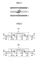
- Fig. 5 is a diagram illustrating a cross section of the directional coupler taken along a line A-A' in Fig. 4.
- a reference numeral 1 is a dielectric substrate having two formation surfaces; reference numerals 2 and 3 are strip conductor patterns (primary line and subsidiary line), each of which is propagated by a high frequency signal; a reference numeral 4 is an ground conductor; reference numerals 5a, 5b, 5c, and 5d are input/output terminals for inputting and outputting a high frequency signal; a reference numeral 6 is a coupled line; a reference numeral 7 represents ground conductor patterns; and a reference numeral 8 represents capacitors (reactive element, capacitive element).
- the strip conductor pattern 2 (a first strip conductor pattern) is formed on one formation surface of the dielectric substrate 1; and the strip conductor pattern 3 (a second strip conductor pattern) is formed on the other formation surface of the dielectric substrate 1.
- the dielectric substrate 1 is sandwiched between the strip conductor patterns 2 and 3.
- the strip conductor pattern 2 has the input/output terminals 5a and 5b; and the strip conductor pattern 3 has the input/output terminals 5c and 5d.
- the strip conductor patterns 2 and 3 are adjacent to each other so that they are electromagnetically coupled in the coupled line 6.
- a length of the coupled line 6 is about 1/4 of a wavelength at a desired frequency.
- each of the formation surfaces of the dielectric substrate 1 is provided with the ground conductor pattern 7.
- the ground conductor patterns 7 of both of the formation surfaces are placed so as not to be opposed to each other.
- Each of the four capacitors 8 is connected between each of lines and each of the ground conductor patterns 7; in this case, each of the lines is connected between each of the input/output terminals 5a, 5b, 5c, 5d and the coupled line 6.
- two ground conductors 4 are placed in parallel at a predetermined distance so as to sandwich the dielectric substrate 1, on which the strip conductor patterns 2 and 3, the ground conductor pattern 7, and the four capacitors 8 are placed. In this manner, the directional coupler according to the first embodiment constitutes a suspended strip line.
- Figs. 6(a) and 6(b) show diagrams, each of which illustrates an equivalent circuit of the coupled line 6, which is provided by the directional coupler shown in Fig. 4; and the capacitors 8.
- Figs. 6(a) and 6(b) show an excitation in an even mode, and an excitation in an odd mode respectively. It should be noted that it is assumed that a loss of the coupled line 6 is disregarded.
- reference numerals 6a and 6b are inductance Le (a reactive component and a series inductive component) per unit length, and capacitance Ce (a reactive component and a parallel capacitive component) per unit length, of the coupled line 6 respectively, which is excited in the even mode.
- reference numerals 6c and 6d are inductance Lo (reactive component and series inductive component) per unit length, and capacitance Co (reactive component and parallel capacitive component), of the coupled lines 6 respectively, which is excited in the odd mode.
- the inductances 6a and 6c are connected in series between the input/output terminals 5a and 5b.
- the capacitances 6b and 6d are connected in parallel so that each of the capacitances 6b and 6d is connected from a line between the input/output terminal 5a and the input/output terminal 5b to the ground.
- the capacitors 8 are connected in parallel so that each of the capacitors 8 is connected from a position between the input/output terminal 5a or 5b and the coupled line 6 to the ground.
- Fig 7 illustrates electric field distribution of the directional coupler shown in Fig. 5; and Figs. 7(a) and 7(b) are a diagram in the even mode and a diagram in the odd mode respectively. Arrows in the diagrams represent electric fields.
- the dielectric substrate 1 has almost no electric field in the even mode shown in Fig. 7(a), whereas electric fields are concentrated on the dielectric substrate 1 in the odd mode shown Fig. 7(b). Because of it, in the odd mode, a wavelength decreasing rate by the dielectric substrate 1 becomes higher than that in the even mode. Therefore, difference in the wavelength shortening rate between these modes causes phase velocity in the odd mode to decrease more than phase velocity in the even mode. In response to the difference in the phase velocity, characteristics of the conventional directional coupler were degraded.
- capacitance equivalently possessed by the coupled line 6 is compensated by providing the capacitors 8, which are connected in parallel so that each of the capacitors 8 is connected from a line between each of the input/output terminals 5a, 5b, 5c, 5d and the coupled line 6 to the ground. This reduces the difference in the phase velocity between the modes, which results in improvement of characteristic degradation of the directional coupler. Reasons for this will be described as below.
- Ve [Le*Ce] -0.5
- Vo [Lo*Co] -0.5
- phase velocity Ve and Vo of the coupled line 6 depends on the product of inductance and capacitance.
- adding the capacitors 8 increases capacitance Ce and Co of the coupled line 6.
- Inductance Le is relatively large and capacitance Ce is small in the even mode. Because of it, when addition of the capacitor 8 causes the capacitance Ce to increase, the phase velocity in the even mode will decrease to a large extent.
- capacitance Co is relatively large and inductance Lo is small in the odd mode. Because of it, even if addition of the capacitor 8 causes the capacitance Co to increase, the phase velocity in the odd mode is not influenced to a large extent.
- Capacitance C of the capacitor 8 should be determined so that a value of the phase velocity in the even mode approximates to a value of the phase velocity in the odd mode as closely as possible.
- characteristic degradation of the directional coupler can be improved by the following method: difference in phase velocity, which has been caused by difference between a wavelength shortening rate in the even mode and a wavelength shortening rate in the odd mode, is compensated by increasing capacitance of the coupled line 6 using the capacitors 8.
- the strip conductor patterns 2 and 3 which are provided on one formation surface and the other formation surface of the dielectric substrate 1 respectively as a primary line and a subsidiary line so as to sandwich the dielectric substrate 1, and which have the coupled line 6 where the strip conductor patterns 2 and 3 are electromagnetically coupled to each other; and the ground conductors 4, which are placed at a predetermined distance so as to sandwich the dielectric substrate 1; the capacitors 8, which are connected in parallel, are provided for the coupled line 6 of the directional coupler.
- Fig. 8 is a diagram illustrating a configuration of a directional coupler according to a second embodiment of the present invention.
- a reference numeral 9 represents open stubs (reactive element and capacitive element), which are provided between each of the input/output terminals 5a, 5b, 5c, 5d and the coupled line 6 respectively.
- open stubs reactive element and capacitive element
- the open stubs 9 are provided in the second embodiment. Adjusting lengths of the open stubs 9 permits the open stubs 9 to work in the same manner as the capacitors 8. Therefore, such a configuration can produce the same effects as the first embodiment.
- Fig. 9 is a diagram illustrating a configuration of a directional coupler according to a third embodiment of the present invention.
- a reference numeral 10 represents low impedance lines (reactive element and capacitive element), which are provided between each of the input/output terminals 5a, 5b, 5c, 5d and the coupled line 6 respectively.
- Like parts are identified by the same reference numerals as in Fig. 4.
- the low impedance lines 10 are provided in the third embodiment.
- the low impedance lines 10 work in the same manner as the capacitors 8. Therefore, such a configuration can produce the same effects as the first embodiment.
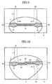
- Fig. 10 is a diagram illustrating a configuration of a directional coupler according to a fourth embodiment of the present invention.
- the directional coupler shown in Fig. 10 has an area 63 (intersection area), where propagating directions of high frequency signals intersect in a decussate form at a center of a projection image of the coupled lines 61 and 62 when each of the strip conductor patterns 2 and 3 is projected from a normal line direction of a formation surface to the same plane parallel to the formation surface of the dielectric substrate 1 (any one of the formation surfaces can be used).
- the coupled lines 61 and 62 have the area 63 where those coupled lines are electromagnetically coupled to each other. Therefore, on the assumption that the area 63 is a boundary, the strip conductor pattern 2 is projected above the strip conductor pattern 3 on the right side of Fig. 10, whereas the strip conductor pattern 3 is projected above the strip conductor pattern 2 on the left side of Fig. 10.
- a length of each coupled line 61 or 62 is about 1/8 of a wavelength in a desired frequency. Therefore, a total length of the coupled lines 61 and 62 becomes about 1/4 of a wavelength. Additionally, degrees of electromagnetic coupling of the coupled lines 61 and 62 are equal.
- the strip conductor patterns 2 and 3 are provided so that those strip conductor patterns intersect between the coupled lines 61 and 62. Connection of the coupled lines 61 and 62 in series works in the same manner as the coupled line 6 shown in the third embodiment. Therefore, such a configuration can produce the same effects as the third embodiment.
- Figs. 11(a) and 11(b) show explanatory diagrams, each of which illustrates effects of the directional coupler of the embodiments according to the present invention. Both of the diagrams magnify the coupled lines 61 and 62 of the directional coupler. Like parts are identified by the same reference numerals as in Fig. 10.
- the coupled lines 61 and 62 have the area 63 where those coupled lines are electromagnetically coupled to each other. Because of it, in the case of Fig. 11(a), the coupled line 62 is loosely coupled whereas the coupled line 61 is tightly coupled. In the case of Fig. 11(b), the coupled line 61 is tightly coupled whereas the coupled line 62 is loosely coupled. Therefore, it is so devised that regardless of a direction of a deviation, a deviation in one degree of coupling can be compensated by a deviation in the other degree of coupling.
- the directional coupler is configured to have an area 63, where propagating directions of a high frequency signal intersect at a center of a projection image of the coupled lines 61 and 62, which are coupled electromagnetically, at the time of projection from a normal line direction of a formation surface of the dielectric substrate 1 to a plane parallel to the formation surface; because of it, even if mutual relative positions of the strip conductor patterns 2 and 3 deviate to a direction parallel to the dielectric substrate 1 and at the same time the mutual relative positions deviate to a direction orthogonal to the propagating direction of the high frequency signal in the coupled line 61 and 62, a deviation in a degree of coupling can be reduced, which enables us to produce the directional coupler easily.
- the fourth embodiment can be applied to the directional couplers (the first, the second, and the third embodiment) in which the strip conductor pattern 2 is formed on one formation surface of the dielectric substrate 1 and the strip conductor pattern 3 is formed on the other formation surface.
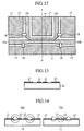
- Fig. 12 is a diagram illustrating a configuration of a directional coupler according to a fifth embodiment of the present invention.
- Fig. 13 is a diagram illustrating a cross section of the directional coupler taken along a line A-A' shown in Fig. 12.
- a reference numeral 11 is a dielectric substrate having two formation surfaces; reference numerals 12 and 13 are strip conductor patterns (primary line and subsidiary line), each of which is propagated by a high frequency signal; reference numerals 15a, 15b, 15c, and 15d are input/output terminals for inputting and outputting a high frequency signal; a reference numeral 16 is a coupled line; a reference numeral 17 represents ground conductor patterns; and a reference numeral 18 represents capacitors (reactive element, capacitive element).
- Both of the strip conductor patterns 12 and 13 are formed on one formation surface of the dielectric substrate 11.
- the strip conductor pattern 12 has the input/output terminals 15a and 15b; and the strip conductor pattern 13 has the input/output terminals 15c and 15d.
- the strip conductor patterns 12 and 13 are adjacent to each other so that they are electromagnetically coupled in the coupled line 16.
- a length of the coupled line 16 is about 1/4 of a wavelength at a desired frequency.
- ground conductor patterns 17 are also formed on the same formation surface of the dielectric substrate 11 as that formed with the strip conductor patterns 12 and 13. In this case, the conductor patterns 17 are placed so as to surround the strip conductor patterns 12 and 13.
- Each of the four capacitors 18 is connected between each of lines and each of the ground conductor patterns 17; in this case, each of lines is connected between each of the input/output terminals 15a, 15b, 15c, 15d, and the coupled line 16.
- the directional coupler according to the fifth embodiment constitutes a coplanar waveguide.
- FIG. 6 an equivalent circuit of the directional coupler according to the fifth embodiment is provided in Fig. 6.
- electric field distribution of the directional coupler which was shown in Fig. 13, is illustrated in Figs. 14(a) and 14(b).
- Fig. 14(a) shows electric field distribution in the even mode
- Fig. 14(b) shows electric field distribution in the odd mode. Arrows in the diagrams represent electric fields.
- Electric field distribution in the even mode of Fig. 14(a) has also a tendency to diffuse into the air among the strip conductor patterns 12, 13 and the ground conductor pattern 17, whereas electric field distribution in the odd mode of Fig. 14(b) concentrates on the inside of the dielectric substrate 11 between the strip conductor patterns 12 and 13, which are adjacent to each other. Therefore, a wavelength shortening rate by the dielectric substrate 11 in the case of the odd mode is higher than that in the case of the even mode, which causes phase velocity in the odd mode to decrease as compared with the even mode, resulting in characteristic degradation of the directional coupler.
- the following effect can be produced: adding the capacitors 18 compensates for the difference in the phase velocity between the modes, which improves the characteristics of the directional coupler.
- the directional coupler comprising: the dielectric substrate 11; the strip conductor patterns 12 and 13 that are formed in one formation surface of the dielectric substrate 11, and that have the coupled line 16 for electromagnetic coupling; and the ground conductor pattern 17 that is formed on one formation surface of the dielectric substrate 11, where the strip conductor patterns 12 and 13 were formed; the capacitors 18, which are connected in parallel, are provided for the coupled line 16 of the directional coupler. Because of it, there is obtained an effect of being capable of compensating for the difference in the phase velocity between the modes, which allows to configure a directional coupler of the coplanar waveguide, of which characteristic degradation is improved.
- the fifth embodiment because all of the strip conductor patterns 12, 13, and the ground conductor pattern 17 are formed in one formation surface of the dielectric substrate 11, the following effect can be obtained: as compared with the first embodiment, it is possible to mount the capacitors 18 more easily.
- the open stub 9 of the second embodiment or the low impedance line 10 of the third embodiment may be used.
- Fig. 15 is a diagram illustrating a configuration of a directional coupler according to a sixth embodiment of the present invention.
- Fig. 16 is a diagram illustrating a cross section of the directional coupler taken along a line A-A' shown in Fig. 15.
- a reference numeral 21 is a dielectric substrate having two formation surfaces; reference numerals 22 and 23 are strip conductor patterns (primary line and subsidiary line), each of which is propagated by a high frequency signal; reference numerals 25a, 25b, 25c, and 25d are input/output terminals for inputting and outputting a high frequency signal; a reference numeral 26 is a coupled line; a reference numeral 27 is an ground conductor pattern; and a reference numeral 28 represents inductors (reactive element, inductive element).
- Both of the strip conductor patterns 22 and 23 are formed on one formation surface of the dielectric substrate 21.
- the strip conductor pattern 22 has the input/output terminals 25a and 25b; and the strip conductor pattern 23 has the input/output terminals 25c and 25d.
- the strip conductor patterns 22 and 23 are adjacent to each other so that they are electromagnetically coupled in the coupled line 26.
- a length of the coupled line 26 is about 1/4 of a wavelength at a desired frequency.
- An ground conductor pattern 27 is provided on the other formation surface that is different from the one formation surface of the dielectric substrate 21 on which the strip conductor patterns 22 and 23 are provided.
- Each of the four inductors 28 is connected between each of the input/output terminals 25a, 25b, 25c, 25d and the coupled line 26 respectively.
- the directional coupler according to the sixth embodiment constitutes a microstrip line.
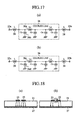
- Figs. 17(a) and 17(b) show diagrams, each of which illustrates an equivalent circuit of the coupled line 26, which is provided by the directional coupler shown in Fig. 15; and the inductors 28.
- Figs. 17(a) and 17(b) show an excitation in an even mode, and an excitation in an odd mode respectively. It should be noted that it is assumed that a loss of the coupled line 26 is disregarded.
- reference numerals 26a and 26b are inductance Le (a reactive component and a series inductive component) per unit length, and capacitance Ce (a reactive component and a parallel capacitive component) per unit length, of the coupled line 26 respectively, which is excited in the even mode.
- reference numerals 26c and 26d are inductance Lo (reactive component and series inductive component) per unit length, and capacitance Co (reactive component and parallel capacitive component), of the coupled line 26 respectively, which is excited in the odd mode.
- the inductances 26a and 26c are connected in series between the input/output terminals 25a and 25b.
- the capacitances 26b and 26d are connected in parallel so that each of the capacitances 26b and 26d is connected from a line between the input/output terminal 25a and the input/output terminal 25b to the ground.
- the inductors 28 are connected in series so that each of the inductors 28 is connected from each of the input/output terminals 25a and 25b to the coupled line 26.
- impedance Ze in the even mode, and impedance Ze in the odd mode, of the coupled line 26 are given by expressions (1a) and (1b) respectively; and phase velocity Ve in the even mode and phase velocity Vo in the odd mode are given by expressions (2a) and (2b) respectively.
- Fig 18 illustrates electric field distribution of the directional coupler shown in Fig. 16; and Figs. 18(a) and 18(b) are a diagram in the even mode and a diagram in the odd mode respectively. Arrows in the diagrams represent electric fields.
- a wavelength shortening rate of the even mode is higher than that in the odd mode.
- inductance component of the coupled line 26 is increased to compensate for the difference in phase velocity between the modes.
- the directional coupler is provided with the inductors 28 that are connected to a line, which is connected between the input/output terminals 25a and 25b, in series to increases inductance of the coupled line 26.
- Inductance of the inductor 28 should be determined so that a value of the phase velocity in the even mode approximates to a value of the phase velocity in the odd mode as closely as possible.
- the directional coupler comprising: the dielectric substrate 21; the strip conductor patterns 22 and 23 that are formed in one formation surface of the dielectric substrate 21, and that have the coupled line 26 for electromagnetic coupling; and an ground conductor pattern 27 formed on the other formation surface that is different from said one formation surface of the dielectric substrate 21 on which the strip conductor patterns 22 and 23 are formed; the inductors 28, which are connected in series, are provided for the coupled line 26 of the directional coupler. Therefore, there is obtained an effect of being capable of configuring a directional coupler of the microstrip line that can decrease the phase velocity in the odd mode without considerable influence on the phase velocity in the even mode, resulting in improvement in characteristic degradation.
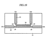
- Fig. 19 is a diagram illustrating a configuration of a directional coupler according to a seventh embodiment of the present invention.
- a reference numeral 29 represents high impedance lines (reactive element and inductive element), which are provided between each of the input/output terminals 25a, 25b, 25c, 25d and the coupled line 26 respectively.
- Like parts are identified by the same reference numerals as in Fig. 15.
- the high impedance lines 29 are provided in the seventh embodiment.
- the high impedance lines 29 work in the same manner as the inductors 28. Therefore, such a configuration can produce the same effects as the fifth embodiment.
- the directional coupler according to the present invention is suitable for a communication system that uses microwaves and millimeter waves, and that couples a high frequency signal, which is inputted in a primary line, with a subsidiary line while realizing good characteristics such as directivity and reflection.
Landscapes
- Waveguides (AREA)
- Control Of Motors That Do Not Use Commutators (AREA)
Abstract
Description
Claims (27)
- A directional coupler comprising: a primary line and a subsidiary line through which a high frequency signal propagates; and a coupled line in which the primary line is electromagnetically coupled to the subsidiary line; said directional coupler comprising:a reactive element that is mounted on the primary line and the subsidiary line, and that compensates for a reactive component equivalently possessed by the coupled line.
- A directional coupler comprising: a dielectric substrate having two formation surfaces; a primary line and a subsidiary line, which are formed on the dielectric substrate, and each of which has an input/output terminal for inputting/outputting a high frequency signal at both ends, and through which the high frequency signal propagates; and a coupled line in which the primary line electromagnetically coupled to the subsidiary line; wherein as compared with electric field distribution in an even mode in which the primary line and the subsidiary line are excited at in-phase equal amplitude, electric field distribution in an odd mode, in which the primary line and the subsidiary line are excited at out-of-phase equal amplitude, concentrates on the inside of the dielectric substrate; said directional coupler comprising:a capacitive element that is mounted on the primary line and the subsidiary line, and that compensates for a parallel capacitive component equivalently possessed by the coupled line.
- A directional coupler according to Claim 2, wherein:the capacitive element is a capacitor that is connected from a position between the input/output terminal and a coupled line to ground.
- A directional coupler according to Claim 2, wherein:the capacitive element is an open stub that is provided between the input/output terminal and the coupled line.
- A directional coupler according to Claim 2, wherein:the capacitive element is a low impedance line that is provided between the input/output terminal and the coupled line.
- A directional coupler according to Claim 2, wherein:the primary line and the subsidiary line have an intersection area where propagating directions of a high frequency signal intersect at a center of the coupled line at the time of projection from a normal line direction of a formation surface to a plane parallel to the formation surface.
- A directional coupler according to Claim 3, wherein:the primary line and the subsidiary line have an intersection area where propagating directions of a high frequency signal intersect at a center of the coupled line at the time of projection from a normal line direction of a formation surface to a plane parallel to the formation surface.
- A directional coupler according to Claim 4, wherein:the primary line and the subsidiary line have an intersection area where propagating directions of a high frequency signal intersect at a center of the coupled line at the time of projection from a normal line direction of a formation surface to a plane parallel to the formation surface.
- A directional coupler according to Claim 5, wherein:the primary line and the subsidiary line have an intersection area where propagating directions of a high frequency signal intersect at a center of the coupled line at the time of projection from a normal line direction of a formation surface to a plane parallel to the formation surface.
- A directional coupler according to Claim 2, wherein:the primary line is provided by a first strip conductor pattern that is formed in one formation surface of a dielectric substrate;the subsidiary line is provided by a second strip conductor pattern that is formed in the other formation surface of the dielectric substrate, which is different from said one formation surface of the dielectric substrate on which the first strip conductor pattern is formed; andsaid directional coupler comprises ground conductors, which are placed at a predetermined distance so as to sandwich the dielectric substrate where a pair of the strip conductor patterns are formed.
- A directional coupler according to Claim 3, wherein:the primary line is provided by a first strip conductor pattern that is formed in one formation surface of a dielectric substrate;the subsidiary line is provided by a second strip conductor pattern that is formed in the other formation surface of the dielectric substrate, which is different from said one formation surface of the dielectric substrate on which the first strip conductor pattern is formed; andsaid directional coupler comprises ground conductors, which are placed at a predetermined distance so as to sandwich the dielectric substrate where a pair of the strip conductor patterns are formed.
- A directional coupler according to Claim 4, wherein:the primary line is provided by a first strip conductor pattern that is formed in one formation surface of a dielectric substrate;the subsidiary line is provided by a second strip conductor pattern that is formed in the other formation surface of the dielectric substrate, which is different from said one formation surface of the dielectric substrate on which the first strip conductor pattern is formed; andsaid directional coupler comprises ground conductors, which are placed at a predetermined distance so as to sandwich the dielectric substrate where a pair of the strip conductor patterns are formed.
- A directional coupler according to Claim 5, wherein:the primary line is provided by a first strip conductor pattern that is formed in one formation surface of a dielectric substrate;the subsidiary line is provided by a second strip conductor pattern that is formed in the other formation surface of the dielectric substrate, which is different from said one formation surface of the dielectric substrate on which the first strip conductor pattern is formed; andsaid directional coupler comprises ground conductors, which are placed at a predetermined distance so as to sandwich the dielectric substrate where a pair of the strip conductor patterns are formed.
- A directional coupler according to Claim 6, wherein:the primary line is provided by a first strip conductor pattern that is formed in one formation surface of a dielectric substrate;the subsidiary line is provided by a second strip conductor pattern that is formed in the other formation surface of the dielectric substrate, which is different from said one formation surface of the dielectric substrate on which the first strip conductor pattern is formed; andsaid directional coupler comprises ground conductors, which are placed at a predetermined distance so as to sandwich the dielectric substrate where a pair of the strip conductor patterns are formed.
- A directional coupler according to Claim 7, wherein:the primary line is provided by a first strip conductor pattern that is formed in one formation surface of a dielectric substrate;the subsidiary line is provided by a second strip conductor pattern that is formed in the other formation surface of the dielectric substrate, which is different from said one formation surface of the dielectric substrate on which the first strip conductor pattern is formed; andsaid directional coupler comprises ground conductors, which are placed at a predetermined distance so as to sandwich the dielectric substrate where a pair of the strip conductor patterns are formed.
- A directional coupler according to Claim 8, wherein:the primary line is provided by a first strip conductor pattern that is formed in one formation surface of a dielectric substrate;the subsidiary line is provided by a second strip conductor pattern that is formed in the other formation surface of the dielectric substrate, which is different from said one formation surface of the dielectric substrate on which the first strip conductor pattern is formed; andsaid directional coupler comprises ground conductors, which are placed at a predetermined distance so as to sandwich the dielectric substrate where a pair of the strip conductor patterns are formed.
- A directional coupler according to Claim 9, wherein:the primary line is provided by a first strip conductor pattern that is formed in one formation surface of a dielectric substrate;the subsidiary line is provided by a second strip conductor pattern that is formed in the other formation surface of the dielectric substrate, which is different from said one formation surface of the dielectric substrate on which the first strip conductor pattern is formed; andsaid directional coupler comprises ground conductors, which are placed at a predetermined distance so as to sandwich the dielectric substrate where a pair of the strip conductor patterns are formed.
- A directional coupler according to Claim 2, wherein:each of the primary line and the subsidiary line is provided by a strip conductor pattern that is formed in one formation surface of a dielectric substrate; andsaid directional coupler comprises an ground conductor that is formed on said one formation surface of the dielectric substrate where the strip conductor pattern is formed.
- A directional coupler according to Claim 3, wherein:each of the primary line and the subsidiary line is provided by a strip conductor pattern that is formed in one formation surface of a dielectric substrate; andsaid directional coupler comprises an ground conductor that is formed on said one formation surface of the dielectric substrate where the strip conductor pattern is formed.
- A directional coupler according to Claim 4, wherein:each of the primary line and the subsidiary line is provided by a strip conductor pattern that is formed in one formation surface of a dielectric substrate; andsaid directional coupler comprises an ground conductor that is formed on said one formation surface of the dielectric substrate where the strip conductor pattern is formed.
- A directional coupler according to Claim 5, wherein:each of the primary line and the subsidiary line is provided by a strip conductor pattern that is formed in one formation surface of a dielectric substrate; andsaid directional coupler comprises an ground conductor that is formed on said one formation surface of the dielectric substrate where the strip conductor pattern is formed.
- A directional coupler comprising: a dielectric substrate having two formation surfaces; a primary line and a subsidiary line, which are formed on the dielectric substrate, and each of which has an input/output terminal for inputting/outputting a high frequency signal at both ends, and through which the high frequency signal propagates; and a coupled line in which the primary line is electromagnetically coupled to the subsidiary line; wherein as compared with electric field distribution in an odd mode in which the primary line and the subsidiary line are excited at out-of-phase equal amplitude, electric field distribution in an even mode, in which the primary line and the subsidiary line are excited at in-phase equal amplitude, concentrates on the inside of the dielectric substrate; said directional coupler comprising:an inductive element that is mounted on the primary line and the subsidiary line, and that compensates for a series inductive component equivalently possessed by the coupled line.
- A directional coupler according to Claim 22, wherein:the inductive element is an inductor that is provided between the input/output terminal and the coupled line.
- A directional coupler according to Claim 22, wherein:the inductive element is a high impedance line that is provided between the input/output terminal and the coupled line.
- A directional coupler according to Claim 22, wherein:each of the primary line and the subsidiary line is provided by a strip conductor pattern that is formed in one formation surface of a dielectric substrate; andsaid directional coupler comprises an ground conductor that is formed on the other formation surface of the dielectric substrate, which is different from said one formation surface of the dielectric substrate where the strip conductor pattern is formed.
- A directional coupler according to Claim 23, wherein:each of the primary line and the subsidiary line is provided by a strip conductor pattern that is formed in one formation surface of a dielectric substrate; andsaid directional coupler comprises an ground conductor that is formed on the other formation surface of the dielectric substrate, which is different from said one formation surface of the dielectric substrate where the strip conductor pattern is formed.
- A directional coupler according to Claim 24, wherein:each of the primary line and the subsidiary line is provided by a strip conductor pattern that is formed in one formation surface of a dielectric substrate; andsaid directional coupler comprises an ground conductor that is formed on the other formation surface of the dielectric substrate, which is different from said one formation surface of the dielectric substrate where the strip conductor pattern is formed.
Applications Claiming Priority (3)
| Application Number | Priority Date | Filing Date | Title |
|---|---|---|---|
| JP2000174287 | 2000-06-09 | ||
| JP2000174287 | 2000-06-09 | ||
| PCT/JP2001/000433 WO2001095426A1 (en) | 2000-06-09 | 2001-01-24 | Directional coupler |
Publications (2)
| Publication Number | Publication Date |
|---|---|
| EP1291959A1 true EP1291959A1 (en) | 2003-03-12 |
| EP1291959A4 EP1291959A4 (en) | 2003-05-28 |
Family
ID=18676359
Family Applications (1)
| Application Number | Title | Priority Date | Filing Date |
|---|---|---|---|
| EP01983269A Withdrawn EP1291959A4 (en) | 2000-06-09 | 2001-01-24 | DIRECTIVE COUPLER |
Country Status (6)
| Country | Link |
|---|---|
| US (1) | US20020113667A1 (en) |
| EP (1) | EP1291959A4 (en) |
| KR (1) | KR20020021678A (en) |
| CN (1) | CN1383590A (en) |
| CA (1) | CA2379262A1 (en) |
| WO (1) | WO2001095426A1 (en) |
Families Citing this family (26)
| Publication number | Priority date | Publication date | Assignee | Title |
|---|---|---|---|---|
| KR20030097533A (en) * | 2002-06-21 | 2003-12-31 | 강인호 | LOW INSERTION LOSS DIRECTIONAL COUPLER USING 3λ/4 EQUIVALENT LUMPED ELEMENT |
| AU2003224574A1 (en) * | 2003-04-25 | 2004-11-23 | Telefonaktiebolaget Lm Ericsson (Publ) | An improved directional coupler |
| US6946927B2 (en) * | 2003-11-13 | 2005-09-20 | Northrup Grumman Corporation | Suspended substrate low loss coupler |
| KR100563790B1 (en) * | 2003-11-27 | 2006-03-30 | 심한식 | Directional Coupler for Mobile Communication |
| KR100623519B1 (en) * | 2004-04-28 | 2006-09-19 | 안달 | High Directivity Microstrip Directional Coupler |
| DE102005016054A1 (en) * | 2005-04-07 | 2006-10-12 | Kathrein-Werke Kg | High-frequency coupler or power divider, in particular narrow-band and / or 3dB coupler or power divider |
| EP1837946B1 (en) | 2006-03-25 | 2012-07-11 | HÜTTINGER Elektronik GmbH + Co. KG | Directional coupler |
| DE102007006225A1 (en) * | 2007-02-08 | 2008-08-14 | Hüttinger Elektronik Gmbh + Co. Kg | Directional coupler for measurement and regulation in high frequency-power which absorbs load, has coupling loss in forward direction and in backward direction |
| FR2916086B1 (en) * | 2007-05-11 | 2010-09-03 | Thales Sa | HYPERFREQUENCY SIGNAL COUPLER IN MICRORUBAN TECHNOLOGY. |
| CN101686068B (en) * | 2008-09-28 | 2013-01-30 | 华为技术有限公司 | Power division network device |
| JP5478102B2 (en) * | 2009-04-08 | 2014-04-23 | 三菱電機株式会社 | High frequency cutoff circuit |
| US8299871B2 (en) * | 2010-02-17 | 2012-10-30 | Analog Devices, Inc. | Directional coupler |
| CN101882704A (en) * | 2010-04-29 | 2010-11-10 | 合肥威科电子技术有限公司 | Novel air cavity bridge for microwave communication |
| US8330552B2 (en) * | 2010-06-23 | 2012-12-11 | Skyworks Solutions, Inc. | Sandwich structure for directional coupler |
| US20120019335A1 (en) * | 2010-07-20 | 2012-01-26 | Hoang Dinhphuoc V | Self compensated directional coupler |
| KR101767293B1 (en) | 2010-07-29 | 2017-08-10 | 스카이워크스 솔루션즈, 인코포레이티드 | Reducing coupling coefficient variation by using capacitors |
| JP2012060614A (en) * | 2010-09-13 | 2012-03-22 | Toshiba Corp | Directional coupler |
| CN102044734B (en) * | 2010-10-18 | 2013-11-13 | 杭州紫光网络技术有限公司 | Identical system circuit combiner with high-isolation degree |
| RU2494502C2 (en) * | 2011-10-18 | 2013-09-27 | Федеральное государственное унитарное предприятие "Ростовский-на-Дону научно-исследовательский институт радиосвязи" (ФГУП "РНИИРС") | Miniature broadband quadrature directional coupler on lumped elements |
| DE112013004185B4 (en) * | 2013-05-06 | 2023-03-30 | Rohde & Schwarz GmbH & Co. Kommanditgesellschaft | directional coupler |
| CN103259071A (en) * | 2013-05-10 | 2013-08-21 | 宜兴亚泰科技有限公司 | Cavity bridge |
| DE102013213981A1 (en) | 2013-07-17 | 2015-01-22 | Rohde & Schwarz Gmbh & Co. Kg | Coil for switching device with high RF power |
| KR101490835B1 (en) * | 2013-07-18 | 2015-02-09 | 주식회사 네이버스 | Broadband coupled line coupler |
| CN105789811A (en) * | 2016-04-20 | 2016-07-20 | 广东工业大学 | Self-compensation directional coupler |
| JP2018088640A (en) * | 2016-11-29 | 2018-06-07 | 株式会社東芝 | Manufacturing method of directional coupler |
| KR102302423B1 (en) * | 2020-10-28 | 2021-09-15 | 한화시스템 주식회사 | Microstrip Directional Coupler |
Family Cites Families (7)
| Publication number | Priority date | Publication date | Assignee | Title |
|---|---|---|---|---|
| JPS4635635Y1 (en) * | 1968-12-28 | 1971-12-08 | ||
| JPS5662402A (en) * | 1979-10-26 | 1981-05-28 | Fujitsu Ltd | Directional coupler |
| GB2218853A (en) * | 1988-05-18 | 1989-11-22 | Philips Electronic Associated | Microwave directional coupler |
| US4902990A (en) * | 1988-09-26 | 1990-02-20 | Hughes Aircraft Company | Thick film microwave coupler |
| US5075646A (en) * | 1990-10-22 | 1991-12-24 | Westinghouse Electric Corp. | Compensated mixed dielectric overlay coupler |
| US5159298A (en) * | 1991-01-29 | 1992-10-27 | Motorola, Inc. | Microstrip directional coupler with single element compensation |
| JPH05191113A (en) * | 1992-01-10 | 1993-07-30 | Fujitsu Ltd | Strip line circuit |
-
2001
- 2001-01-24 WO PCT/JP2001/000433 patent/WO2001095426A1/en not_active Ceased
- 2001-01-24 KR KR1020027001492A patent/KR20020021678A/en not_active Ceased
- 2001-01-24 US US10/048,922 patent/US20020113667A1/en not_active Abandoned
- 2001-01-24 CA CA002379262A patent/CA2379262A1/en not_active Abandoned
- 2001-01-24 CN CN01801660A patent/CN1383590A/en active Pending
- 2001-01-24 EP EP01983269A patent/EP1291959A4/en not_active Withdrawn
Also Published As
| Publication number | Publication date |
|---|---|
| WO2001095426A1 (en) | 2001-12-13 |
| CA2379262A1 (en) | 2001-12-13 |
| CN1383590A (en) | 2002-12-04 |
| KR20020021678A (en) | 2002-03-21 |
| EP1291959A4 (en) | 2003-05-28 |
| US20020113667A1 (en) | 2002-08-22 |
Similar Documents
| Publication | Publication Date | Title |
|---|---|---|
| EP1291959A1 (en) | Directional coupler | |
| EP0885469B1 (en) | A high frequency balun provided in a multilayer substrate | |
| US7777589B2 (en) | Balun transformer | |
| US8305283B2 (en) | Coplanar differential bi-strip delay line, higher-order differential filter and filtering antenna furnished with such a line | |
| US7432786B2 (en) | High frequency filter | |
| EP3624187A1 (en) | Impendance control unit | |
| KR20020013940A (en) | Balun | |
| JP2007013809A (en) | High frequency balun | |
| US20100225416A1 (en) | Multi-Section Velocity Compensated Microstrip Directional Coupler | |
| JPH08162812A (en) | High frequency coupler | |
| JP2003264404A (en) | In-band group delay flattening circuit and distortion compensation type amplifier | |
| JP2906863B2 (en) | Stripline dual mode filter | |
| TWI851086B (en) | Common mode filter and signal transmission circuit | |
| JPH0130321B2 (en) | ||
| EP1019976A1 (en) | Slot line band pass filter | |
| JPWO2001095426A1 (en) | directional coupler | |
| US7463120B2 (en) | High frequency filter | |
| JPH08195606A (en) | Microwave coupled line | |
| JP3823390B2 (en) | Signal synthesis circuit | |
| JP2006238063A (en) | Directional coupler | |
| CN118676562A (en) | Common mode filter and signal transmission circuit | |
| WO2019155624A1 (en) | Balun and antenna power supply circuit | |
| JP3872200B2 (en) | Non-radiative dielectric line coupler | |
| US20040178866A1 (en) | Band rejection filter with attenuation poles | |
| JP3023945B2 (en) | High frequency filter |
Legal Events
| Date | Code | Title | Description |
|---|---|---|---|
| PUAI | Public reference made under article 153(3) epc to a published international application that has entered the european phase |
Free format text: ORIGINAL CODE: 0009012 |
|
| 17P | Request for examination filed |
Effective date: 20020117 |
|
| AK | Designated contracting states |
Kind code of ref document: A1 Designated state(s): AT BE CH CY DE DK ES FI FR GB GR IE IT LI LU MC NL PT SE TR Designated state(s): AT BE CH CY DE DK ES FI FR GB GR IE IT LI LU MC NL PT SE TR |
|
| AX | Request for extension of the european patent |
Extension state: AL LT LV MK RO SI |
|
| A4 | Supplementary search report drawn up and despatched |
Effective date: 20030416 |
|
| STAA | Information on the status of an ep patent application or granted ep patent |
Free format text: STATUS: THE APPLICATION HAS BEEN WITHDRAWN |
|
| 18W | Application withdrawn |
Effective date: 20031103 |
|
| RBV | Designated contracting states (corrected) |
Designated state(s): DE FI FR SE |