EP1291682A1 - Optical waveguide type diffraction grating and method for manufacturing the same - Google Patents
Optical waveguide type diffraction grating and method for manufacturing the same Download PDFInfo
- Publication number
- EP1291682A1 EP1291682A1 EP01930209A EP01930209A EP1291682A1 EP 1291682 A1 EP1291682 A1 EP 1291682A1 EP 01930209 A EP01930209 A EP 01930209A EP 01930209 A EP01930209 A EP 01930209A EP 1291682 A1 EP1291682 A1 EP 1291682A1
- Authority
- EP
- European Patent Office
- Prior art keywords
- light
- cutoff
- optical waveguide
- refractive index
- diffraction grating
- Prior art date
- Legal status (The legal status is an assumption and is not a legal conclusion. Google has not performed a legal analysis and makes no representation as to the accuracy of the status listed.)
- Withdrawn
Links
Images





Classifications
-
- G—PHYSICS
- G02—OPTICS
- G02B—OPTICAL ELEMENTS, SYSTEMS OR APPARATUS
- G02B6/00—Light guides; Structural details of arrangements comprising light guides and other optical elements, e.g. couplings
- G02B6/02—Optical fibres with cladding with or without a coating
- G02B6/02057—Optical fibres with cladding with or without a coating comprising gratings
- G02B6/02076—Refractive index modulation gratings, e.g. Bragg gratings
- G02B6/02123—Refractive index modulation gratings, e.g. Bragg gratings characterised by the method of manufacture of the grating
- G02B6/02133—Refractive index modulation gratings, e.g. Bragg gratings characterised by the method of manufacture of the grating using beam interference
- G02B6/02138—Refractive index modulation gratings, e.g. Bragg gratings characterised by the method of manufacture of the grating using beam interference based on illuminating a phase mask
-
- G—PHYSICS
- G02—OPTICS
- G02B—OPTICAL ELEMENTS, SYSTEMS OR APPARATUS
- G02B6/00—Light guides; Structural details of arrangements comprising light guides and other optical elements, e.g. couplings
- G02B6/10—Light guides; Structural details of arrangements comprising light guides and other optical elements, e.g. couplings of the optical waveguide type
- G02B6/12—Light guides; Structural details of arrangements comprising light guides and other optical elements, e.g. couplings of the optical waveguide type of the integrated circuit kind
- G02B2006/12083—Constructional arrangements
- G02B2006/12107—Grating
-
- G—PHYSICS
- G02—OPTICS
- G02B—OPTICAL ELEMENTS, SYSTEMS OR APPARATUS
- G02B6/00—Light guides; Structural details of arrangements comprising light guides and other optical elements, e.g. couplings
- G02B6/02—Optical fibres with cladding with or without a coating
- G02B6/02057—Optical fibres with cladding with or without a coating comprising gratings
- G02B6/02076—Refractive index modulation gratings, e.g. Bragg gratings
- G02B6/0208—Refractive index modulation gratings, e.g. Bragg gratings characterised by their structure, wavelength response
- G02B6/02085—Refractive index modulation gratings, e.g. Bragg gratings characterised by their structure, wavelength response characterised by the grating profile, e.g. chirped, apodised, tilted, helical
Definitions
- the present invention relates to a diffraction grating device in which a diffraction grating is formed in an optical waveguide region of an optical waveguide, and a method of making such a diffraction grating device.
- a diffraction grating device is one in which a diffraction grating is formed in an optical waveguide region of an optical waveguide.
- the optical waveguide is one in which a cladding region having a low refractive index is disposed about a core region having a high refractive index, and can cause an optical waveguide region including the core region to guide light.
- This optical waveguide includes not only an optical fiber but also a planar optical waveguide formed on a flat substrate.
- the optical waveguide is based on silica glass (SiO 2 ), whereas its core region is doped with an additive (e.g., GeO 2 ) adapted to raise the refractive index.
- the silica glass doped with GeO 2 raises its refractive index when irradiated with refractive index change inducing light having a predetermined wavelength (e.g., KrF excimer laser light having a wavelength of 248 nm).
- a predetermined wavelength e.g., KrF excimer laser light having a wavelength of 248 nm.
- the diffraction grating device is made. Namely, an optical waveguide, based on silica glass, having an optical waveguide region doped with GeO 2 is prepared, and one surface of a phase grating made of a transparent flat plate in which projections and depressions having a predetermined period are formed is arranged so as to come into nearly close contact with the surface of the optical waveguide.
- refractive index change inducing light is made incident on the phase grating, whereby interference fringes between +first-order diffracted light and -first-order diffracted light are formed in the optical waveguide region.
- a refractive index modulated area is generated in the optical waveguide region of optical waveguide according to the optical energy distribution of interference fringes, whereby the diffraction grating device is made.
- Such a diffraction grating device is used as an optical filter, for example. Namely, the diffraction grating device blocks by a large cutoff amount a light component in a cutoff wavelength band including a Bragg wavelength (cutoff peak wavelength) ⁇ B in the light having reached the refractive index modulated area after being guided through the optical waveguide region, while transmitting therethrough light components to be transmitted in wavelength bands other than the cutoff wavelength band.
- a diffraction grating device adapted to transmit the signal light therethrough but block the monitor light is provided in front of a receiver, so that the signal light reaches the receiver whereas the monitor light does not reach the receiver.
- a diffraction grating device not only blocks light in the cutoff wavelength band including the cutoff peak wavelength ⁇ B but also somewhat blocks light in the wavelength band of 0.9 ⁇ B to 0.95 ⁇ B originally meant to be transmitted therethrough.
- diffraction grating devices used in optical communication systems for guiding the signal light and monitor light can block the monitor light by a sufficient cutoff amount
- they also somewhat block the signal light originally meant to be transmitted since the signal light is attenuated by the diffraction grating device, the signal light reaching a receiver lowers its power, whereby reception errors may occur in extreme cases.
- Adiffraction grating device intended to overcome such a problem is disclosed in Japanese Patent Application Laid-Open No. HEI 11-326672.
- the diffraction grating device disclosed in this publication is one in which a refractive index modulated area is formed in an optical fiber of single-peak type having a core surrounded by a cladding and exhibiting a refractive index distribution form of ⁇ -th power profile ( ⁇ ⁇ 1.5).
- ⁇ -th power profile ⁇ -th power profile
- the diffraction grating device disclosed in the above-mentioned publication is one in which a refractive index modulated area is formed not in an optical fiber having a usual refractive index of stepped index type, but in an optical fiber having a special ⁇ -th power profile, which is not easy to make and yields a low mass-productivity. Also, the cutoff amount in the wavelength band of 0.9 ⁇ B to 0.95 ⁇ B originally meant to be transmitted is not sufficiently low.
- ⁇ B is a cutoff peak wavelength
- the method of making a diffraction grating device in accordance with the present invention comprises the steps of preparing an optical waveguide having an optical waveguide region doped with an additive adapted to generate a refractive index change upon irradiation with refractive index change inducing light having a predetermined wavelength, and a phase grating having a predetermined projection and depression pattern; separating the optical waveguide and the phase grating from each other by a distance yielding a predetermined optical path difference between zero-order transmitted light and second-order diffracted light of the refractive index change inducing light such that a modulation intensity of interference light between the zero-order transmitted light and second-order diffracted light becomes 85% or less of that obtained when no optical path difference exists between the zero-order transmitted light and second-order diffracted light; and making the refractive index change inducing light incident on the phase grating, so as to form an interference fringe of first-order diffracted light in the optical waveguide region of the optical waveguide, thereby forming the optical
- phase grating When refractive index change inducing light having a predetermined wavelength is made incident on a phase grating, not only first-order diffracted light but also zero-order transmitted light and higher-order (second-order or higher) diffracted light are generated from the phase grating.
- light in the wavelength band of 0.9 ⁇ B to 0.95 ⁇ B originally meant to be transmitted has been blocked due to components of the refractive index modulation based on interference fringes between the zero-order transmitted light and higher-order diffracted light, interference fringes between the zero-order transmitted light and second-order diffracted light in particular.
- the optical waveguide and the phase grating are separated from each other as mentioned above, so that components of the refractive index modulation based on interference fringes between the zero-order transmitted light and second-order diffracted light are weak, whereby the cutoff amount in the wavelength band of 0.9 ⁇ B to 0.95 ⁇ B becomes smaller.
- the diffraction grating device in accordance with the present invention is made by the above-mentioned method of making a diffraction grating device in accordance with the present invention.
- it exhibits a cutoff amount of at least 20 dB in a cutoff wavelength band having a width of at least 15 nm including a cutoff peak wavelength ⁇ B , and a cutoff amount of 1 dB or less in the wavelength band of 0.9 ⁇ B to 0.95 ⁇ B .
- a diffraction grating device is favorably used, for example, in an optical communication system in which the cutoff peak wavelength ⁇ B is at a monitor light wavelength of 1650 nm whereas the signal light wavelength is in the 1550-nm wavelength band.
- the inventors have found that light in the wavelength band of 0.9 ⁇ B to 0.95 ⁇ B is presumed to be blocked due to components of the refractive index modulation based on interference fringes between the zero-order transmitted light and higher-order (second-order or higher) diffracted light from the phase grating, interference fringes between the zero-order transmitted light and second-order diffracted light in particular, in the conventional diffraction grating devices.
- the inventors studied the relationship between the optical distance from the phase grating surface to the optical axis center of optical waveguide and the optical path difference between the zero-order transmitted light and second-order diffracted light affecting the cutoff amount in the wavelength band of 0.9 ⁇ B to 0.95 ⁇ B .
- the optical path difference between the zero-order transmitted light and second-order diffracted light depends on the angle of diffraction of the zero-order transmitted light and second-order diffracted light, and varies according to the period of the phase grating employed. Assuming that the diffracted light beams have the positional relationship shown in Fig.
- ⁇ and a indicate the wavelength of incident light and the mask period, respectively.
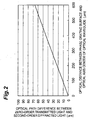
- the relationship between the optical path difference between the zero-order transmitted light and second-order diffracted light and the optical distance from the phase grating surface to the optical axis center of optical waveguide is determined.
- the optical path difference between the zero-order transmitted light and second-order diffracted light is required to be at least 30 ⁇ m in order for the optical distance between the phase grating surface and the optical axis center of optical waveguide to become at least 250 ⁇ m.
- the spectrum P(k) is expressed by: where k is the wave number of light, k cen is the optical center wavelength, and ⁇ k is the optical frequency width.
- the wave number of light k is expressed as 1/ ⁇ by using the wavelength ⁇ of laser light.
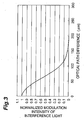
- the modulation intensity of interference light of laser light is represented by the curve shown in Fig. 3 from expressions (1) and (2).
- the abscissa indicates the optical path difference x, whereas the ordinate indicates the normalized modulation intensity of interference light. From Fig. 3, it has been seen that, when the optical path difference is at least 30 ⁇ m, the modulation intensity of interference light of laser light became 85% or less of that obtained when the optical path difference was 0.
- a diffraction grating whose cutoff amount is sufficiently small in the wavelength band of 0.9 ⁇ B to 0.95 ⁇ B can easily be formed if refractive index change inducing light is made incident on a phase grating while an optical waveguide and the phase grating are separated from each other by a distance yielding a predetermined optical path difference between zero-order transmitted light and second-order diffracted light of the refractive index change inducing light such that the modulation intensity of interference light between the zero-order transmitted light and second-order diffracted light becomes 85% or less of that obtained when the optical path difference between the zero-order transmitted light and second-order diffracted light is 0, thus attaining the present invention.
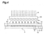
- FIG. 4 is an explanatory view of the method of making a diffraction grating device in accordance with this embodiment.
- This drawing shows respective cross sections of an optical fiber 10 and a phase grating 20.
- the optical fiber 10 is one in which a cladding region 12 having a low refractive index is disposed about a core region 11 having a high refractive index, and can cause an optical waveguide region including the core region 11 to guide light.
- the optical fiber 10 is based on silica glass (SiO 2 ), whereas the core region 11 is doped with GeO 2 .
- GeO 2 is not only an additive adapted to raise the refractive index of the core region 11 when simply added thereto, but also an additive adapted to further raise the refractive index of the core region 11 when irradiated with refractive index change inducing light having a predetermined wavelength.
- the refractive index change inducing light is KrF excimer laser light (having a wavelength of 248 nm) or the second harmonic (having a wavelength of 244 nm) of argon ion laser, for example.
- the phase grating 20 is a transmission diffraction grating of phase modulation type made of a flat silica glass plate one surface of which is formed with projections and depressions having a predetermined period.
- the period of projections and depressions in the phase grating 20 is designed so as to become twice that of the refractive index modulation to be formed in the core region 11 of optical fiber 10.
- the phase grating 20 is disposed parallel to the optical fiber 10 such that its surface formed with projections and depressions faces the optical fiber 10.
- the optical axis center of core region 11 of optical fiber 10 and the surface of phase grating 20 formed with projections and depressions are separated from each other by an optical distance D.
- the optical distance D is set to a distance yielding a predetermined optical path difference between zero-order transmitted light and second-order diffracted light of the refractive index change inducing light such that the modulation intensity of interference light between the zero-order transmitted light and second-order diffracted light becomes 85% or less of that obtained when the optical path difference between the zero-order transmitted light and second-order diffracted light is 0.
- the upper limit of optical distance D is a distance by which the ⁇ first-order diffracted light forming the Bragg wavelength does not reach the core region 11 of optical fiber 10.
- the upper limit D max of optical distance D is 22.4 mm.
- the beam diameter is restricted, and the optical distance becomes shorter than the upper limit in order to attain a desirable grating length when the time for forming gratings is taken into consideration.
- the refractive index change inducing light is made incident on the phase grating 20, so as to form interference fringes of refractive index change inducing light in the core region 11 of optical fiber 10.
- refractive index change inducing light A is made incident on the phase grating 20 at right angles, so as to generate +first-order diffracted light A +1 and -first-order diffracted light A -1 from the phase grating 20, whereby interference fringes of the +first-order diffracted light A +1 and -first-order diffracted light A -1 are formed in the core region 11.
- a refractive index modulation corresponding to the optical energy distribution of interference fringes is generated in the core region 11, so as to make a diffraction grating device 1 having a cutoff peak wavelength ⁇ B .
- the optical distance D is set to a value falling within the above-mentioned range, the numeric range of the above-mentioned expression (1) in particular, so that components of the refractive index modulation based on interference fringes between the zero-order transmitted light and second-order diffracted light are weak, whereby the cutoff amount in the wavelength band of 0.9 ⁇ B to 0.95 ⁇ B becomes smaller.
- a diffraction grating device having a wide cutoff band with a cutoff bandwidth of 20 nm including a cutoff peak wavelength ⁇ B was prepared.
- the phase grating 20 one having a mask period of 1.138 ⁇ m was used.
- the cutoff peak wavelength ⁇ B was set to 1650 nm.
- Fig. 6 is a view showing the loss spectrum of a diffraction grating device made such that the distance between the optical fiber surface and the phase grating surface was 100 ⁇ m.
- Fig. 7 is a view showing the loss spectrum of a diffraction grating device made such that the distance between the optical fiber surface and the phase grating surface was 300 ⁇ m. When the distance between the optical fiber surface and the phase grating surface was 100 ⁇ m, as can be seen from Fig.
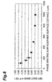
- Fig. 8 is a graph showing the relationship between the distance between the optical fiber surface and phase grating surface and the loss peak value at a wavelength of 1520 nm.
- the distance between the optical fiber surface and phase grating surface was set so as to fall within the range of 100 ⁇ m to 1000 ⁇ m.
- the loss peak value became lower at a wavelength of 1520 nm within the transmission wavelength band of 0.9 ⁇ B to 0.95 ⁇ B as the distance is longer in this distance range.
- the loss peak value at a wavelength of 1520 nm within the transmission wavelength band was 1 dB or less when the distance between the optical fiber surface and phase grating surface was 150 ⁇ m or greater.
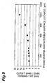
- Fig. 9 is a graph showing the relationship between the distance between the optical fiber surface and phase grating surface and the irradiation time of refractive index change inducing light required for the cutoff amount at the cutoff peak wavelength ⁇ B to become at least 30 dB.
- the distance between the optical fiber surface and phase grating surface was set so as to fall within the range of 100 ⁇ m to 1000 ⁇ m.
- a cutoff amount of 30 dB or greater was obtained at the cutoff peak wavelength ⁇ B within this distance range.
- the irradiation time of refractive index change inducing light required for the cutoff amount at the cutoff peak wavelength ⁇ B to become at least 30 dB became longer as the distance was longer.
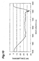
- Fig. 10 is a view showing the transmission spectrum of a diffraction grating device made such that the distance between the optical fiber surface and phase grating surface was 100 ⁇ m.
- Fig. 11 is a view showing the transmission spectrum of a diffraction grating device made such that the distance between the optical fiber surface and phase grating surface was 1000 ⁇ m.
- the cutoff amount was at least 20 dB in a wavelength band (about 1641 nm to about 1662 nm) including the cutoff peak wavelength ⁇ B in either of the cases where the distance between the optical fiber surface and phase grating surface was 100 ⁇ m and 1000 ⁇ m.
- the cutoff amount was at least 30 dB in a wavelength band (about 1643 nm to about 1662 nm) including the cutoff peak wavelength ⁇ B .
- a diffraction grating device 1 having a narrow cutoff wavelength band with a cutoff wavelength bandwidth of 0.4 nm including the cutoff peak wavelength was prepared.
- the phase grating 20 one having a mask period of 1.138 ⁇ m was used.
- Fig. 12 is a view showing the transmission spectrum of a diffraction grating device made such that the distance between the optical fiber surface and phase grating surface was 100 ⁇ m.
- the cutoff peak wavelength ⁇ B at that time was 1651.4 nm.
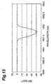
- Fig. 13 is a view showing the transmission spectrum of a diffraction grating device made such that the distance between the optical fiber surface and phase grating surface was 600 ⁇ m.
- the cutoff peak wavelength ⁇ B at that time was 1651.7 nm.
- the cutoff amount was at least 20 dB in a wavelength band (about 1651.2 nm to about 1651.6 nm) including the cutoff peak wavelength ⁇ B when the distance between the optical fiber surface and phase grating surface was 100 ⁇ m. Also, the cutoff amount was at least 30 dB in a wavelength band (about 1651.3 nm to about 1651.5 nm) including the cutoff peak wavelength ⁇ B . As can be seen from Fig. 13, the cutoff amount was at least 20 dB in a wavelength band (about 1651.5 nm to about 1651.9 nm) including the cutoff peak wavelength ⁇ B when the distance between the optical fiber surface and phase grating surface was 600 ⁇ m. Also, the cutoff amount was at least 30 dB in a wavelength band (about 1651.6 nm to about 1651.8 nm) including the cutoff peak wavelength ⁇ B .
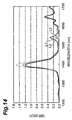
- Fig. 14 is a graph showing loss spectrum (cutoff amounts) around the transmission wavelength band of 0.9 ⁇ B to 0.95 ⁇ B in cases where the distance between the optical fiber surface and phase grating surface is 100 ⁇ m (indicated by L1), 300 ⁇ m (indicated by L2), and 600 ⁇ m (indicated by L3), respectively.
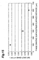
- Fig. 15 is a graph showing the relationship between the radiation loss and the distance from the phase grating to the optical fiber surface in the vicinity of 1.52- ⁇ m wavelength band when the transmission wavelength band is 0.9 ⁇ B to 0.95 ⁇ B .
- the radiation loss in the vicinity of the 1.52- ⁇ m wavelength band is at least 0.3 dB when the distance between the optical fiber surface and phase grating surface is 100 ⁇ m
- the radiation loss in the vicinity of the 1.52- ⁇ m wavelength band is suppressed so as to become less than 0.2 dB when the distance between the optical fiber surface and phase grating surface is elongated to 300 ⁇ m and 600 ⁇ m.
- the radius r of optical fiber is 62.5 ⁇ m, whereas the refractive index n of optical fiber at a wavelength of 248 nm is 1.51.
- the optical distance between the optical axis center of core region in the optical fiber and the phase grating surface is adjusted appropriately, so as to fall within the numerical range of the above-mentioned expression (1) in particular, whereby thus made diffraction grating device can sufficiently lower the cutoff amount in the wavelength band of 0.9 ⁇ B to 0.95 ⁇ B originally meant to be transmitted, while fully securing the cutoff amount in the cutoff wavelength band including the cutoff peak wavelength ⁇ B .
- a refractive index modulation is formed by use of an optical fiber having a normal refractive index profile of stepped index type, the making is easy, and the mass-productivity is excellent.
- the method of making a diffraction grating device in accordance with this embodiment can make a diffraction grating device exhibiting a cutoff amount of at least 20 dB in a cutoff wavelength band having a width of at least 15 nm including the cutoff peak wavelength ⁇ B , and a cutoff amount of 1 dB or less in the wavelength band of cutoff wavelength band 0.9 ⁇ B to 0.95 ⁇ B .
- a diffraction grating device exhibiting a cutoff amount of at least 20 dB in a cutoff wavelength band having a width of at least 0.2 nm including the cutoff peak wavelength ⁇ B , and a cutoff amount of 0.2 dB or less in the wavelength band of cutoff wavelength band 0.9 ⁇ B to 0.95 ⁇ B .
- the diffraction grating device in accordance with this embodiment designed so as to have a cutoff peak wavelength at the monitor light wavelength of 1650 nm is disposed in front of a receiver.
- the diffraction grating device can block the monitor light by a cutoff amount of 20 dB or greater, so as to keep it from reaching the receiver.
- the diffraction grating device allows the signal light to reach the receiver with a cutoff amount of 1 dB or less, so that the signal light reaching the receiver has a sufficient power, thereby lowering the risk of generating reception errors.
- the method of making a diffraction grating device in accordance with the present invention can make a diffraction grating device having a sufficiently small cutoff amount in the wavelength band of 0.9 ⁇ B to 0.95 ⁇ B originally meant to be transmitted, while fully securing a cutoff amount in a cutoff wavelength band including the cutoff peak wavelength ⁇ B . Also, since it will be sufficient if a refractive index modulation is formed by use of an optical fiber having a normal refractive index profile of stepped index type, the making is easy, and the mass-productivity can be improved.
Landscapes
- Physics & Mathematics (AREA)
- Engineering & Computer Science (AREA)
- Manufacturing & Machinery (AREA)
- General Physics & Mathematics (AREA)
- Optics & Photonics (AREA)
- Diffracting Gratings Or Hologram Optical Elements (AREA)
- Optical Fibers, Optical Fiber Cores, And Optical Fiber Bundles (AREA)
- Optical Integrated Circuits (AREA)
Abstract
Description
| Order of | 0 | 1 | 2 |
| Angle of diffraction i (deg) | 0.0 | 12.6 | 25.8 |

Claims (4)
- Amethod of making a diffraction grating device comprising the steps of:preparing an optical waveguide having an optical waveguide region doped with an additive adapted to generate a refractive index change upon irradiation with refractive index change inducing light having a predetermined wavelength, and a phase grating having a predetermined projection and depression pattern;separating said optical waveguide and said phase grating from each other by a distance yielding a predetermined optical path difference between zero-order transmitted light and second-order diffracted light of said refractive index change inducing light such that amodulation intensity of interference light between said zero-order transmitted light and second-order diffracted light becomes 85% or less of that obtained when no optical path difference exists between said zero-order transmitted light and second-order diffracted light; andmaking said refractive index change inducing light incident on said phase grating, so as to form an interference fringe of first-order diffracted light in said optical waveguide region of said optical waveguide, thereby forming said optical waveguide region with a diffraction grating.
- Adiffraction grating device made by the method of making a diffraction grating device according to claim 1.
- Adiffraction grating device according to claim 2, exhibiting a cutoff amount of at least 20 dB in a cutoff wavelength band having a width of at least 15 nm including a cutoff peak wavelength λB, and a cutoff amount of 1 dB or less in a wavelength band of 0.9λB to 0.95λB.
- Adiffraction grating device according to claim 2, exhibiting a cutoff amount of at least 20 dB in a cutoff wavelength band having a width of at least 0.2 nm including a cutoff peak wavelength λB, and a cutoff amount of 0.2 dB or less in a wavelength band of 0.9λB to 0.95λB.
Applications Claiming Priority (3)
| Application Number | Priority Date | Filing Date | Title |
|---|---|---|---|
| JP2000146790 | 2000-05-18 | ||
| JP2000146790 | 2000-05-18 | ||
| PCT/JP2001/004171 WO2001088573A1 (en) | 2000-05-18 | 2001-05-18 | Optical waveguide type diffraction grating and method for manufacturing the same |
Publications (2)
| Publication Number | Publication Date |
|---|---|
| EP1291682A1 true EP1291682A1 (en) | 2003-03-12 |
| EP1291682A4 EP1291682A4 (en) | 2005-07-20 |
Family
ID=18653072
Family Applications (1)
| Application Number | Title | Priority Date | Filing Date |
|---|---|---|---|
| EP01930209A Withdrawn EP1291682A4 (en) | 2000-05-18 | 2001-05-18 | OPTICAL WAVEGUIDE TYPE DIFFRACTION NETWORK AND METHOD OF MANUFACTURING THE SAME |
Country Status (5)
| Country | Link |
|---|---|
| US (1) | US20030113065A1 (en) |
| EP (1) | EP1291682A4 (en) |
| AU (1) | AU5677601A (en) |
| TW (1) | TW569041B (en) |
| WO (1) | WO2001088573A1 (en) |
Families Citing this family (6)
| Publication number | Priority date | Publication date | Assignee | Title |
|---|---|---|---|---|
| US20090016686A1 (en) * | 2007-07-13 | 2009-01-15 | Nufern | Optical fiber gratings for handling increased power levels and methods of making |
| DE102008063225A1 (en) | 2008-12-23 | 2010-07-01 | Carl Zeiss Meditec Ag | Device for Swept Source Optical Coherence Domain Reflectometry |
| US9234998B2 (en) * | 2013-01-29 | 2016-01-12 | Corning Incorporated | Optical fiber with a low-index core and a core grating |
| JP6387964B2 (en) * | 2013-09-02 | 2018-09-12 | Agc株式会社 | Measuring device |
| CN103487239B (en) * | 2013-10-11 | 2015-11-25 | 杭州奥普特光学有限公司 | Hand-held eyeglass surface focal power measurement device |
| US11747376B2 (en) * | 2021-04-01 | 2023-09-05 | City University Of Hong Kong | Photonic device and a terahertz signal generator |
Family Cites Families (10)
| Publication number | Priority date | Publication date | Assignee | Title |
|---|---|---|---|---|
| US5367588A (en) * | 1992-10-29 | 1994-11-22 | Her Majesty The Queen In Right Of Canada, As Represented By The Minister Of Communications | Method of fabricating Bragg gratings using a silica glass phase grating mask and mask used by same |
| US5712715A (en) * | 1992-12-23 | 1998-01-27 | Lucent Technologies Inc. | Optical transmission system with spatially-varying Bragg reflector |
| US5327515A (en) * | 1993-01-14 | 1994-07-05 | At&T Laboratories | Method for forming a Bragg grating in an optical medium |
| JP3845922B2 (en) * | 1996-12-05 | 2006-11-15 | 住友電気工業株式会社 | Manufacturing method of optical waveguide type diffraction grating |
| US6289154B1 (en) * | 1997-11-04 | 2001-09-11 | The Furukawa Electric Co., Ltd. | Grating-type optical component and method of manufacturing the same |
| JP3203641B2 (en) * | 1998-06-26 | 2001-08-27 | 住友電気工業株式会社 | Optical loss filter |
| EP1092165A4 (en) * | 1998-07-01 | 2005-06-22 | Corning Inc | Apodization of optical filters formed in photosensitive media |
| JP2000321963A (en) * | 1999-03-10 | 2000-11-24 | Victor Co Of Japan Ltd | Volume hologram recording method |
| JP3955703B2 (en) * | 1999-12-22 | 2007-08-08 | 昭和電線デバイステクノロジー株式会社 | Fabrication method of fiber grating |
| US6553163B2 (en) * | 2000-03-30 | 2003-04-22 | Corning, Incorporated | Method and apparatus for writing a Bragg grating in a waveguide |
-
2001
- 2001-05-18 EP EP01930209A patent/EP1291682A4/en not_active Withdrawn
- 2001-05-18 WO PCT/JP2001/004171 patent/WO2001088573A1/en not_active Ceased
- 2001-05-18 TW TW090111930A patent/TW569041B/en not_active IP Right Cessation
- 2001-05-18 US US10/258,958 patent/US20030113065A1/en not_active Abandoned
- 2001-05-18 AU AU56776/01A patent/AU5677601A/en not_active Abandoned
Also Published As
| Publication number | Publication date |
|---|---|
| WO2001088573A1 (en) | 2001-11-22 |
| EP1291682A4 (en) | 2005-07-20 |
| US20030113065A1 (en) | 2003-06-19 |
| TW569041B (en) | 2004-01-01 |
| AU5677601A (en) | 2001-11-26 |
Similar Documents
| Publication | Publication Date | Title |
|---|---|---|
| EP0793123B1 (en) | Optical signal shaping device for complex spectral shaping applications | |
| EP0629885A1 (en) | Optical waveguiding component comprising a band-pass filter | |
| US6178045B1 (en) | Spatial filter for high power laser beam | |
| EP0893712A2 (en) | Diffraction grating type bandpass filter and method of making the same | |
| EP3457183B1 (en) | Multicore optical fiber, fiber bragg grating, and method for manufacturing a fiber bragg grating | |
| EP0840147A2 (en) | Method and apparatus for making continuous chirped fiber bragg gratings | |
| EP1121613A1 (en) | Apparatus for manufacturing long-period fiber gratings and apparatus for manufacturing two-band long-period fiber gratings using the same | |
| US6084996A (en) | Broadband long-period gratings | |
| EP1500959A1 (en) | Optical fiber and fiber-grating filter comprising same | |
| US20030113065A1 (en) | Optical waveguide type diffraction grating and method for manufacturing the same | |
| EP1406098A1 (en) | Optical waveguide diffraction grating device and its fabrication method | |
| US6950576B1 (en) | Mode coupling devices with complex spectral profile | |
| EP3876003B1 (en) | Slant-type fiber grating | |
| EP1326103B1 (en) | Optical waveguide diffraction grating | |
| US6253008B1 (en) | Optical filter and method of making the same | |
| US6289154B1 (en) | Grating-type optical component and method of manufacturing the same | |
| US6766080B2 (en) | Optical waveguide type defraction grating device and a method of manufacturing thereof | |
| JP2000275442A (en) | Optical bandpass filter | |
| CN102177455B (en) | Light transmitting receiving module | |
| JP5340197B2 (en) | Optical filter, manufacturing method thereof and designing method thereof | |
| JP3955703B2 (en) | Fabrication method of fiber grating | |
| AU2002301376B2 (en) | Apparatus for manufacturing two-band long-period fiber gratings using the same | |
| JPWO2001088573A1 (en) | Optical waveguide diffraction grating and its manufacturing method | |
| JP2006243400A (en) | Fiber grating manufacturing method and manufacturing apparatus | |
| JP2003322732A (en) | Phase grating mask and method and apparatus for manufacturing optical waveguide type diffraction grating element |
Legal Events
| Date | Code | Title | Description |
|---|---|---|---|
| PUAI | Public reference made under article 153(3) epc to a published international application that has entered the european phase |
Free format text: ORIGINAL CODE: 0009012 |
|
| 17P | Request for examination filed |
Effective date: 20021118 |
|
| AK | Designated contracting states |
Designated state(s): AT BE CH CY DE DK ES FI FR GB GR IE IT LI LU MC NL PT SE TR Kind code of ref document: A1 Designated state(s): AT BE CH CY DE DK ES FI FR GB GR IE IT LI LU MC NL PT SE TR |
|
| RBV | Designated contracting states (corrected) |
Designated state(s): AT BE CH CY DE DK FR GB IE IT LI |
|
| A4 | Supplementary search report drawn up and despatched |
Effective date: 20050603 |
|
| 17Q | First examination report despatched |
Effective date: 20050615 |
|
| STAA | Information on the status of an ep patent application or granted ep patent |
Free format text: STATUS: THE APPLICATION IS DEEMED TO BE WITHDRAWN |
|
| 18D | Application deemed to be withdrawn |
Effective date: 20051026 |