EP1289130A1 - Amplifier circuit apparatus and method therefor - Google Patents
Amplifier circuit apparatus and method therefor Download PDFInfo
- Publication number
- EP1289130A1 EP1289130A1 EP01307437A EP01307437A EP1289130A1 EP 1289130 A1 EP1289130 A1 EP 1289130A1 EP 01307437 A EP01307437 A EP 01307437A EP 01307437 A EP01307437 A EP 01307437A EP 1289130 A1 EP1289130 A1 EP 1289130A1
- Authority
- EP
- European Patent Office
- Prior art keywords
- transistor
- emitter
- transistors
- coupled
- breakdown voltage
- Prior art date
- Legal status (The legal status is an assumption and is not a legal conclusion. Google has not performed a legal analysis and makes no representation as to the accuracy of the status listed.)
- Withdrawn
Links
- 238000000034 method Methods 0.000 title claims description 11
- 230000015556 catabolic process Effects 0.000 claims abstract description 24
- GPXJNWSHGFTCBW-UHFFFAOYSA-N Indium phosphide Chemical compound [In]#P GPXJNWSHGFTCBW-UHFFFAOYSA-N 0.000 claims abstract description 12
- 238000004891 communication Methods 0.000 claims abstract description 10
- 230000008878 coupling Effects 0.000 claims abstract description 3
- 238000010168 coupling process Methods 0.000 claims abstract description 3
- 238000005859 coupling reaction Methods 0.000 claims abstract description 3
- 230000007850 degeneration Effects 0.000 claims description 23
- 229910000577 Silicon-germanium Inorganic materials 0.000 claims description 8
- LEVVHYCKPQWKOP-UHFFFAOYSA-N [Si].[Ge] Chemical compound [Si].[Ge] LEVVHYCKPQWKOP-UHFFFAOYSA-N 0.000 claims description 5
- JBRZTFJDHDCESZ-UHFFFAOYSA-N AsGa Chemical compound [As]#[Ga] JBRZTFJDHDCESZ-UHFFFAOYSA-N 0.000 claims description 4
- 229910001218 Gallium arsenide Inorganic materials 0.000 claims description 4
- 238000005516 engineering process Methods 0.000 abstract description 6
- 239000000463 material Substances 0.000 abstract description 3
- 230000003287 optical effect Effects 0.000 abstract description 3
- 239000004065 semiconductor Substances 0.000 abstract description 3
- 239000003990 capacitor Substances 0.000 description 3
- 235000012431 wafers Nutrition 0.000 description 3
- 238000004519 manufacturing process Methods 0.000 description 2
- 230000007423 decrease Effects 0.000 description 1
- 238000013461 design Methods 0.000 description 1
- 238000011161 development Methods 0.000 description 1
- 230000018109 developmental process Effects 0.000 description 1
- 238000010586 diagram Methods 0.000 description 1
- 230000000694 effects Effects 0.000 description 1
- 230000005670 electromagnetic radiation Effects 0.000 description 1
- 230000007774 longterm Effects 0.000 description 1
- 238000005259 measurement Methods 0.000 description 1
- 229910052710 silicon Inorganic materials 0.000 description 1
- 239000010703 silicon Substances 0.000 description 1
Images
Classifications
-
- H—ELECTRICITY
- H03—ELECTRONIC CIRCUITRY
- H03F—AMPLIFIERS
- H03F3/00—Amplifiers with only discharge tubes or only semiconductor devices as amplifying elements
- H03F3/04—Amplifiers with only discharge tubes or only semiconductor devices as amplifying elements with semiconductor devices only
- H03F3/08—Amplifiers with only discharge tubes or only semiconductor devices as amplifying elements with semiconductor devices only controlled by light
Definitions
- the present invention relates to an amplifier circuit apparatus of the type used as a pre-amplifier for an electrical signal received from a photodiode, for example a photodiode in a receiver in a communications system.
- the present invention also relates to a method of preventing application of a voltage in excess of a predetermined level across a transistor in the amplifier circuit.
- Gain devices namely transistors, forming part of a pre-amplifier circuit within a receiver circuit in an optical communications system have cut-off frequencies that correspond to a maximum bit rate that can be supported by the transistors in the pre-amplifier circuit. Consequently, as the maximum bit rate increases, the peak cut-off frequency of the transistors in the pre-amplifier circuit needs to increase as well. However, as the peak cut-off frequency of the transistors increases, it is known that the breakdown voltage of the transistors decreases. It is common practice in the art to use the BV ce0 measurement between the collector and the emitter terminals of the transistor in order to quantify the breakdown voltage.
- the receiver circuit comprises a photodiode reverse bias coupled to the pre-amplifier circuit
- a minimum reverse bias voltage typically in the range of 1.5V to 1.8V approximately, needs to be maintained across the photodiode in order to ensure correct operation of the photodiode.
- the supply voltage is typically approximately between 3.3V and 3.6V
- known Common-emitter, single transistor, Cascade and Darlington pair pre-amplifier configurations result in a voltage being applied across one or more transistor, forming part of the pre-amplifier circuit, that exceeds the breakdown voltage of the transistor(s). Consequently, the transistor(s) can fail as a result of the application of the excessive voltage across the transistor(s).
- the above prior art pre-amplifier configurations make insufficient voltage headroom available to adequately deplete the photodiode in the presence of such low supply voltages.
- InP Indium Phosphide
- SiGe Silicon Germanium
- InP transistors constitute a relatively new, and as yet, unproven technology. Wafers formed from InP are physically more fragile than wafers formed from SiGe. Additionally, InP technology is currently not susceptible of mass production and has not been proven to be long-term reliable, for example over a period of 20 or more years. These disadvantages, coupled with the expense of such devices to some transceiver manufacturers makes the use of InP transistors less attractive than other technologies. In contrast, SiGe transistors constitute a proven technology that can be produced in high yields, i.e. on approximately 8 inch (approximately 200 mm) wafers.
- an amplifier circuit apparatus for a communications transceiver comprising: a first transistor having a first base, a first emitter for receiving an input signal from a photodiode and coupled to a first emitter degeneration resistor, and a first collector for providing an output signal constituting an amplified version of the input signal; a second transistor coupled in parallel with the first transistor, the second transistor having a second base coupled to the first base for application of a reference signal to the first and second bases and a second emitter coupled to a second emitter degeneration resistor; and a breakdown voltage of the first transistor being less than 2.5V.
- the first and second transistors are bipolar transistors, for example Heterojunction Bipolar Transistors (HBTs) or Bipolar Junction Transistors (BJTs).
- the first transistor is one of a Silicon Germanium transistor, a Gallium Arsenide transistor, or an Indium Phosphide transistor.
- the breakdown voltage is 2.1V or less. More preferably, the breakdown voltage is 2V or less. Very preferably, the breakdown voltage is 1.8V or less.
- a communications transceiver comprises the amplifier circuit apparatus as set forth above.
- a method of preventing application of a voltage in excess of a predetermined level across a first transistor in an amplifier circuit comprising the steps of: coupling a first common emitter degeneration resistor to the first transistor, the first transistor having a first base, a first emitter arranged to receive an input current, and a first collector for providing an output signal constituting an amplified version of the input signal; providing a second transistor coupled in parallel with the first common emitter circuit, the second transistor having a second base coupled to the first base for application of a reference signal to the first and second bases, and a second emitter coupled to a second emitter degeneration resistor; causing a first current to flow though the second transistor and the second emitter, the second transistor and the second emitter degeneration resistor serving to limit a second current flowing through the first emitter of the first transistor to substantially a difference between the first current and the input current.
- a breakdown voltage of the first transistor is less than 2.5V. 15. More preferably, the breakdown voltage is 2.1V or less. Very preferably, the breakdown voltage is 2V or less. Most preferably, the breakdown voltage is less than 1.8V.
- the first and second transistors are bipolar transistors, for example Heterojunction Bipolar Transistors (HBTs) or Bipolar Junction Transistors (BJTs).
- the first transistor is one of a Silicon Germanium transistor, a Gallium Arsenide transistor, or an Indium Phosphide transistor.
- a pre-amplifier circuit 100 comprises a first supply rail 108 for supplying a first supply voltage V cc .
- a first collector resistor 106 has a first terminal thereof coupled to the first supply rail 108, a second terminal of the first collector resistor 106 being coupled to a first collector terminal of a first NPN Bipolar Junction Transistor (BJT) 110 and a first output terminal 111.
- An emitter terminal of the first transistor 110 is coupled to a first input terminal 112 for receiving an input signal generated by a photodiode114.
- An anode of the photodiode 114 is coupled to the first input terminal 112 and an anode of the photodiode 114 is coupled to a first terminal of a load resistor 116 and a first terminal of a capacitor 102.
- a second terminal of the load resistor 116 is coupled to the first supply rail 108.
- a supply rail alternate to the first supply rail 108 can be used.
- a second terminal of the capacitor 102 is coupled to a second supply rail 120 for supplying a second supply voltage V ee , the second supply voltage V ee being at a lower potential than the first supply voltage V cc .
- the capacitor 102 in combination with the load resistor 116 form an RC filter to filter the supply to the photodiode 114.
- the emitter terminal of the first transistor 110 is also coupled to a first terminal of a first emitter degeneration resistor 118, a second terminal of the first emitter degeneration resistor 118 being coupled to the second supply rail 120.
- a base terminal of the first transistor 110 is coupled to a second input terminal 122.
- a second NPN BJT 124 has a base terminal coupled to the second input terminal 122, thereby constituting a common base input stage.
- a collector terminal of the second transistor 124 is coupled to a first terminal of a second collector resistor 126 and a second output terminal 127, a second terminal of the second collector resistor 126 being coupled to the first supply rail 108.
- An emitter terminal of the second transistor 124 is coupled to a first terminal of a second emitter degeneration resistor 128, a second terminal of the second emitter degeneration resistor 128 being coupled to the second supply rail 120.
- the values of the first and second emitter degeneration resistors 118, 128 are selected so that between about 100mV and 1 Volt is dropped across the first and second emitter degeneration resistors 118, 128.
- the values of the first and second collector resistors 106, 126 are selected to be between about one and three times the values of the first and second emitter degeneration resistors 118, 128.
- an input reference voltage V IREF is applied to the second input terminal 122 to bias the first and second transistors 110, 124 to draw between about 1mA and 5mA.
- the application of V IREF results in a first current I 1 flowing through the second emitter degeneration resistor 128 and a second current I 2 flowing through the first emitter degeneration resistor 118. Since the first current I 1 flows through the second emitter degeneration resistor 128, a first collector current flows through the second collector resistor 126 resulting in a first voltage drop thereacross. Similarly, since the second current I 2 flows through the first emitter degeneration resistor 118, a second collector current flows through the first collector resistor 106 resulting in a second voltage drop thereacross.
- a reference output voltage V OREF is present at the second output terminal 127 and corresponds to a difference between the supply voltage V cc and the first voltage drop.
- an output voltage V O1 is present at the first output terminal 111 and corresponds to a difference between the supply voltage V cc and the second voltage drop.
- the output voltage V O1 constitutes an amplified version of an input current flowing through the first input terminal 112.
- a photodiode current I P flows through the photodiode 114 and, consequently, through the first input terminal 112. Since the first input reference voltage V IREF is applied between the base terminals of the first and second transistor 110, 124 and the second supply rail 120, a first voltage applied across the first and second emitter degeneration resistors 118, 128 is substantially the same. Consequently, the first and second currents I 1 ,I 2 remain substantially the same.
- the first transistor 118 is forced to permit less current to flow through the emitter terminal thereof, the current flowing through the emitter terminal of the first transistor 110 corresponding substantially to the difference between the second current I 2 and the photodiode current I P .
- the second collector current flowing through the collector of the first transistor 110 and hence the first collector resistor 106 is also reduced resulting in the first voltage drop across the first collector resistor 106 to reduce as well.
- the output voltage V O1 between the first output terminal 111 and the second supply rail 120 increases.
- a corresponding reduction in the photodiode current I p results in a reduction of the output voltage V O1 .
- V O1 R C I P + V OREF
Landscapes
- Engineering & Computer Science (AREA)
- Power Engineering (AREA)
- Amplifiers (AREA)
Abstract
Description
- The present invention relates to an amplifier circuit apparatus of the type used as a pre-amplifier for an electrical signal received from a photodiode, for example a photodiode in a receiver in a communications system. The present invention also relates to a method of preventing application of a voltage in excess of a predetermined level across a transistor in the amplifier circuit.
- Developments in optical communication systems are being focussed, inter alia, on achieving increasingly higher bit rates. In this respect, communication systems operating at bit rates of 10 Gbps are already achievable, and efforts are being made to increase the bit rate further to 40 Gbps. Gain devices, namely transistors, forming part of a pre-amplifier circuit within a receiver circuit in an optical communications system have cut-off frequencies that correspond to a maximum bit rate that can be supported by the transistors in the pre-amplifier circuit. Consequently, as the maximum bit rate increases, the peak cut-off frequency of the transistors in the pre-amplifier circuit needs to increase as well. However, as the peak cut-off frequency of the transistors increases, it is known that the breakdown voltage of the transistors decreases. It is common practice in the art to use the BVce0 measurement between the collector and the emitter terminals of the transistor in order to quantify the breakdown voltage.
- If the receiver circuit comprises a photodiode reverse bias coupled to the pre-amplifier circuit, a minimum reverse bias voltage, typically in the range of 1.5V to 1.8V approximately, needs to be maintained across the photodiode in order to ensure correct operation of the photodiode. Given that the supply voltage is typically approximately between 3.3V and 3.6V, known Common-emitter, single transistor, Cascade and Darlington pair pre-amplifier configurations result in a voltage being applied across one or more transistor, forming part of the pre-amplifier circuit, that exceeds the breakdown voltage of the transistor(s). Consequently, the transistor(s) can fail as a result of the application of the excessive voltage across the transistor(s). Additionally, since one design goal is to reduce the supply voltage as much as technically feasible, the above prior art pre-amplifier configurations make insufficient voltage headroom available to adequately deplete the photodiode in the presence of such low supply voltages.
- Current trends in the art are therefore to seek a different semiconductor material to enable fabrication of transistors capable of supporting the 40 Gbps bit rate, and that do not suffer from low breakdown, typically BVce0 of the transistors is greater than 2.5V. The search for the different semiconductor material has resulted in the proposed use of Indium Phosphide (InP) transistors to form pre-amplifier circuits. InP transistors are capable of high bandwidths necessary for 40 Gbps and possess a relatively high breakdown voltage as compared with other types of transistors, for example Silicon or Silicon Germanium (SiGe) transistors.
- Accompanying the advantages of speed and high breakdown voltages for transistors formed from InP, is the disadvantage that InP transistors constitute a relatively new, and as yet, unproven technology. Wafers formed from InP are physically more fragile than wafers formed from SiGe. Additionally, InP technology is currently not susceptible of mass production and has not been proven to be long-term reliable, for example over a period of 20 or more years. These disadvantages, coupled with the expense of such devices to some transceiver manufacturers makes the use of InP transistors less attractive than other technologies. In contrast, SiGe transistors constitute a proven technology that can be produced in high yields, i.e. on approximately 8 inch (approximately 200 mm) wafers.
- According to the present invention, there is provided an amplifier circuit apparatus for a communications transceiver, comprising: a first transistor having a first base, a first emitter for receiving an input signal from a photodiode and coupled to a first emitter degeneration resistor, and a first collector for providing an output signal constituting an amplified version of the input signal; a second transistor coupled in parallel with the first transistor, the second transistor having a second base coupled to the first base for application of a reference signal to the first and second bases and a second emitter coupled to a second emitter degeneration resistor; and a breakdown voltage of the first transistor being less than 2.5V.
- Very preferably, the first and second transistors are bipolar transistors, for example Heterojunction Bipolar Transistors (HBTs) or Bipolar Junction Transistors (BJTs). Most preferably, the first transistor is one of a Silicon Germanium transistor, a Gallium Arsenide transistor, or an Indium Phosphide transistor.
- Preferably, the breakdown voltage is 2.1V or less. More preferably, the breakdown voltage is 2V or less. Very preferably, the breakdown voltage is 1.8V or less.
- In a preferred embodiment, a communications transceiver comprises the amplifier circuit apparatus as set forth above.
- According to the present invention, there is also provided a method of preventing application of a voltage in excess of a predetermined level across a first transistor in an amplifier circuit, the method comprising the steps of: coupling a first common emitter degeneration resistor to the first transistor, the first transistor having a first base, a first emitter arranged to receive an input current, and a first collector for providing an output signal constituting an amplified version of the input signal; providing a second transistor coupled in parallel with the first common emitter circuit, the second transistor having a second base coupled to the first base for application of a reference signal to the first and second bases, and a second emitter coupled to a second emitter degeneration resistor; causing a first current to flow though the second transistor and the second emitter, the second transistor and the second emitter degeneration resistor serving to limit a second current flowing through the first emitter of the first transistor to substantially a difference between the first current and the input current.
- Preferably, a breakdown voltage of the first transistor is less than 2.5V. 15. More preferably, the breakdown voltage is 2.1V or less. Very preferably, the breakdown voltage is 2V or less. Most preferably, the breakdown voltage is less than 1.8V.
- Preferably, the first and second transistors are bipolar transistors, for example Heterojunction Bipolar Transistors (HBTs) or Bipolar Junction Transistors (BJTs). Most preferably, the first transistor is one of a Silicon Germanium transistor, a Gallium Arsenide transistor, or an Indium Phosphide transistor.
- It is thus possible to provide an amplifier circuit for a communications transceiver using transistors formed from a proven technology that, despite the restriction of a low breakdown voltage, does not damage the transistor during normal operation. Additionally, sufficient voltage headroom is available to permit adequate depletion of a photodiode.
- At least one embodiment of the invention will now be described, by way of example only, with reference to the accompanying drawing, in which:
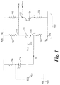
- Figure 1 is a schematic diagram of a pre-amplifier circuit constituting an embodiment of the present invention.
-
- Referring to Figure 1, a
pre-amplifier circuit 100 comprises afirst supply rail 108 for supplying a first supply voltage Vcc. Afirst collector resistor 106 has a first terminal thereof coupled to thefirst supply rail 108, a second terminal of thefirst collector resistor 106 being coupled to a first collector terminal of a first NPN Bipolar Junction Transistor (BJT) 110 and afirst output terminal 111. An emitter terminal of thefirst transistor 110 is coupled to afirst input terminal 112 for receiving an input signal generated by a photodiode114. An anode of thephotodiode 114 is coupled to thefirst input terminal 112 and an anode of thephotodiode 114 is coupled to a first terminal of aload resistor 116 and a first terminal of acapacitor 102. A second terminal of theload resistor 116 is coupled to thefirst supply rail 108. However, a supply rail, alternate to thefirst supply rail 108 can be used. A second terminal of thecapacitor 102 is coupled to asecond supply rail 120 for supplying a second supply voltage Vee, the second supply voltage Vee being at a lower potential than the first supply voltage Vcc. Thecapacitor 102 in combination with theload resistor 116 form an RC filter to filter the supply to thephotodiode 114. - The emitter terminal of the
first transistor 110 is also coupled to a first terminal of a first emitter degeneration resistor 118, a second terminal of the first emitter degeneration resistor 118 being coupled to thesecond supply rail 120. A base terminal of thefirst transistor 110 is coupled to asecond input terminal 122. - A second NPN BJT 124 has a base terminal coupled to the
second input terminal 122, thereby constituting a common base input stage. A collector terminal of the second transistor 124 is coupled to a first terminal of asecond collector resistor 126 and asecond output terminal 127, a second terminal of thesecond collector resistor 126 being coupled to thefirst supply rail 108. An emitter terminal of the second transistor 124 is coupled to a first terminal of a secondemitter degeneration resistor 128, a second terminal of the secondemitter degeneration resistor 128 being coupled to thesecond supply rail 120. - In this example, it should be understood that the values of the first and second
emitter degeneration resistors 118, 128 are selected so that between about 100mV and 1 Volt is dropped across the first and secondemitter degeneration resistors 118, 128. The values of the first andsecond collector resistors emitter degeneration resistors 118, 128. - In operation, an input reference voltage VIREF is applied to the
second input terminal 122 to bias the first andsecond transistors 110, 124 to draw between about 1mA and 5mA. The application of VIREF results in a first current I1 flowing through the secondemitter degeneration resistor 128 and a second current I2 flowing through the first emitter degeneration resistor 118. Since the first current I1 flows through the secondemitter degeneration resistor 128, a first collector current flows through thesecond collector resistor 126 resulting in a first voltage drop thereacross. Similarly, since the second current I2 flows through the first emitter degeneration resistor 118, a second collector current flows through thefirst collector resistor 106 resulting in a second voltage drop thereacross. - As a result of the first voltage drop, a reference output voltage VOREF is present at the
second output terminal 127 and corresponds to a difference between the supply voltage Vcc and the first voltage drop. Similarly, an output voltage VO1 is present at thefirst output terminal 111 and corresponds to a difference between the supply voltage Vcc and the second voltage drop. The output voltage VO1 constitutes an amplified version of an input current flowing through thefirst input terminal 112. - Hence, upon incidence of electromagnetic radiation upon a window (not shown) of the
photodiode 114, a photodiode current IP flows through thephotodiode 114 and, consequently, through thefirst input terminal 112. Since the first input reference voltage VIREF is applied between the base terminals of the first andsecond transistor 110, 124 and thesecond supply rail 120, a first voltage applied across the first and secondemitter degeneration resistors 118, 128 is substantially the same. Consequently, the first and second currents I1 ,I2 remain substantially the same. Given that I2 remains unchanged in the presence of the photodiode current Ip and a component of the second current I2 is the photodiode current Ip, the first transistor 118 is forced to permit less current to flow through the emitter terminal thereof, the current flowing through the emitter terminal of thefirst transistor 110 corresponding substantially to the difference between the second current I2 and the photodiode current IP. As the current flowing through the emitter terminal of thefirst transistor 110 is reduced, the second collector current flowing through the collector of thefirst transistor 110 and hence thefirst collector resistor 106 is also reduced resulting in the first voltage drop across thefirst collector resistor 106 to reduce as well. By reducing the first voltage drop across thefirst collector resistor 106, the output voltage VO1 between thefirst output terminal 111 and thesecond supply rail 120 increases. A corresponding reduction in the photodiode current Ip results in a reduction of the output voltage VO1. - Ignoring second order effects, the output voltage VO1 is given by the following equation:
- An expression for the voltage gain or Transimpedance of the
pre-amplifier circuit 100 is obtained by taking the first derivative of the output voltage VO1 with respect to the photodiode current IP:second collector resistors
Claims (12)
- An amplifier circuit apparatus (100) for a communications transceiver, comprising:a first transistor (110) having a first base, a first emitter for receiving an input signal from a photodiode (116) and coupled to a first emitter degeneration resistor (118), and a first collector for providing an output signal constituting an amplified version of the input signal;a second transistor (124) coupled in parallel with the first transistor (110), the second transistor (124) having a second base coupled to the first base for application of a reference signal to the first and second bases, and a second emitter coupled to a second emitter degeneration resistor (128); anda breakdown voltage of the first transistor (110) being less than 2.5V.
- An apparatus as claimed in Claim 1, wherein the first and second transistors (110, 124) are bipolar transistors .
- An apparatus as claimed in Claim 1 or Claim 2, wherein the first transistor is one of a Silicon Germanium transistor, a Gallium Arsenide transistor, or an Indium Phosphide transistor.
- An apparatus as claimed in any one of the preceding claims, wherein the breakdown voltage is 2.1V or less.
- An apparatus as claimed in Claim 4, wherein the breakdown voltage is 2V or less.
- A communications transceiver comprising the amplifier circuit apparatus (100) as claimed in any one of the preceding claims.
- A method of preventing application of a voltage in excess of a predetermined level across a first transistor (110) in an amplifier circuit (100), the method comprising the steps of:coupling a first emitter degeneration resistor (118) to the first transistor (110), the first transistor (110) having a first base, a first emitter arranged to receive an input current (IP), and a first collector for providing an output signal constituting an amplified version of the input signal;providing a second transistor (124) coupled in parallel with the first transistor (110), the second transistor (124) having a second base coupled to the first base for application of a reference signal to the first and second bases, and a second emitter coupled to a second emitter degeneration resistor (128);causing a first current to flow though the second transistor (124) and the second emitter degeneration resistor (128), the second transistor (124) and the second emitter degeneration resistor (128) serving to limit a second current flowing through the first emitter of the first transistor (110) to substantially a difference between the first current and the input current.
- A method as claimed in Claim 7, wherein a first breakdown voltage of the first transistor is less than 2.5V.
- A method as claimed in Claim 7 or Claim 8, wherein the first and second transistors are bipolar transistors .
- A method as claimed in any one of Claims 7 to 9, wherein the first transistor is one of a Silicon Germanium transistor, a Gallium Arsenide transistor, or an Indium Phosphide transistor.
- A method as claimed in any one of Claims 7 to 10, wherein the breakdown voltage is 2.1V or less.
- A method as claimed in Claim 11, wherein the breakdown voltage is 2V or less.
Priority Applications (1)
| Application Number | Priority Date | Filing Date | Title |
|---|---|---|---|
| EP01307437A EP1289130A1 (en) | 2001-08-31 | 2001-08-31 | Amplifier circuit apparatus and method therefor |
Applications Claiming Priority (1)
| Application Number | Priority Date | Filing Date | Title |
|---|---|---|---|
| EP01307437A EP1289130A1 (en) | 2001-08-31 | 2001-08-31 | Amplifier circuit apparatus and method therefor |
Publications (1)
| Publication Number | Publication Date |
|---|---|
| EP1289130A1 true EP1289130A1 (en) | 2003-03-05 |
Family
ID=8182230
Family Applications (1)
| Application Number | Title | Priority Date | Filing Date |
|---|---|---|---|
| EP01307437A Withdrawn EP1289130A1 (en) | 2001-08-31 | 2001-08-31 | Amplifier circuit apparatus and method therefor |
Country Status (1)
| Country | Link |
|---|---|
| EP (1) | EP1289130A1 (en) |
Cited By (1)
| Publication number | Priority date | Publication date | Assignee | Title |
|---|---|---|---|---|
| CN114374316A (en) * | 2022-01-09 | 2022-04-19 | 王仲季 | A power supply circuit with negative feedback of emitter current |
Citations (2)
| Publication number | Priority date | Publication date | Assignee | Title |
|---|---|---|---|---|
| EP0736967A2 (en) * | 1995-04-07 | 1996-10-09 | Nec Corporation | A preamplifier |
| US6218905B1 (en) * | 1998-11-30 | 2001-04-17 | Vitesse Semiconductor | Common-gate transimpedance amplifier with dynamically controlled input impedance |
-
2001
- 2001-08-31 EP EP01307437A patent/EP1289130A1/en not_active Withdrawn
Patent Citations (2)
| Publication number | Priority date | Publication date | Assignee | Title |
|---|---|---|---|---|
| EP0736967A2 (en) * | 1995-04-07 | 1996-10-09 | Nec Corporation | A preamplifier |
| US6218905B1 (en) * | 1998-11-30 | 2001-04-17 | Vitesse Semiconductor | Common-gate transimpedance amplifier with dynamically controlled input impedance |
Cited By (2)
| Publication number | Priority date | Publication date | Assignee | Title |
|---|---|---|---|---|
| CN114374316A (en) * | 2022-01-09 | 2022-04-19 | 王仲季 | A power supply circuit with negative feedback of emitter current |
| CN114374316B (en) * | 2022-01-09 | 2025-06-06 | 王仲季 | A power supply circuit with emitter current negative feedback |
Similar Documents
| Publication | Publication Date | Title |
|---|---|---|
| US6864751B1 (en) | Transimpedance amplifier with adjustable output amplitude and wide input dynamic-range | |
| US10333479B2 (en) | Power amplifier with improved linearity | |
| US8427227B2 (en) | Temperature compensation circuit | |
| US20030197563A1 (en) | Amplification circuit and optical communication apparatus provided with the amplification circuit | |
| US10326416B2 (en) | Amplifier | |
| JP2018170763A (en) | Trans-impedance amplifier with fast overdrive recovery function | |
| JP2007221490A (en) | Rf power module using heterojunction bipolar transistor | |
| JPH07147520A (en) | Transimpedance type amplifier circuit | |
| US7057462B2 (en) | Temperature compensated on-chip bias circuit for linear RF HBT power amplifiers | |
| CN113452331A (en) | Controllable dynamic bias power amplifier | |
| US6556082B1 (en) | Temperature compensated current mirror | |
| US7920026B2 (en) | Amplifier output stage with extended operating range and reduced quiescent current | |
| Masuda et al. | 40 Gb/s analog IC chipset for optical receiver using SiGe HBTs | |
| US6879214B2 (en) | Bias circuit with controlled temperature dependence | |
| US20080240735A1 (en) | Symmetrical Optical Receiver | |
| US6566955B1 (en) | High bandwidth transresistance amplifier | |
| JPH09186659A (en) | Amplifier circuit | |
| US6529076B2 (en) | Fast saturation recovery operational amplifier input stage | |
| US12021489B2 (en) | Amplifier circuit for driving electro-optical modulators with reduced process, voltage and temperature (PVT) sensitivity | |
| US6879608B1 (en) | High compliance laser driver | |
| US10491163B1 (en) | Fast turn-on amplification system | |
| US8054128B2 (en) | Current control mechanism for low voltage applications | |
| US6507242B1 (en) | Gain switching scheme for amplifiers with digital automatic gain control | |
| US20240283419A1 (en) | Transimpedance gain control | |
| KR100918789B1 (en) | Image Display Devices, Integrated Circuits, and Driver Circuits |
Legal Events
| Date | Code | Title | Description |
|---|---|---|---|
| PUAI | Public reference made under article 153(3) epc to a published international application that has entered the european phase |
Free format text: ORIGINAL CODE: 0009012 |
|
| AK | Designated contracting states |
Kind code of ref document: A1 Designated state(s): AT BE CH CY DE DK ES FI FR GB GR IE IT LI LU MC NL PT SE TR Designated state(s): AT BE CH CY DE DK ES FI FR GB GR IE IT LI LU MC NL PT SE TR |
|
| AX | Request for extension of the european patent |
Extension state: AL LT LV MK RO SI |
|
| AKX | Designation fees paid | ||
| REG | Reference to a national code |
Ref country code: DE Ref legal event code: 8566 |
|
| STAA | Information on the status of an ep patent application or granted ep patent |
Free format text: STATUS: THE APPLICATION IS DEEMED TO BE WITHDRAWN |
|
| 18D | Application deemed to be withdrawn |
Effective date: 20030906 |