EP1288801A2 - Method for designing arithmetic device allocation - Google Patents
Method for designing arithmetic device allocation Download PDFInfo
- Publication number
- EP1288801A2 EP1288801A2 EP02256052A EP02256052A EP1288801A2 EP 1288801 A2 EP1288801 A2 EP 1288801A2 EP 02256052 A EP02256052 A EP 02256052A EP 02256052 A EP02256052 A EP 02256052A EP 1288801 A2 EP1288801 A2 EP 1288801A2
- Authority
- EP
- European Patent Office
- Prior art keywords
- arithmetic
- arithmetic device
- circuit
- operations
- arithmetic operation
- Prior art date
- Legal status (The legal status is an assumption and is not a legal conclusion. Google has not performed a legal analysis and makes no representation as to the accuracy of the status listed.)
- Withdrawn
Links
Images








Classifications
-
- G—PHYSICS
- G06—COMPUTING OR CALCULATING; COUNTING
- G06F—ELECTRIC DIGITAL DATA PROCESSING
- G06F30/00—Computer-aided design [CAD]
- G06F30/30—Circuit design
-
- G—PHYSICS
- G06—COMPUTING OR CALCULATING; COUNTING
- G06F—ELECTRIC DIGITAL DATA PROCESSING
- G06F7/00—Methods or arrangements for processing data by operating upon the order or content of the data handled
- G06F7/38—Methods or arrangements for performing computations using exclusively denominational number representation, e.g. using binary, ternary, decimal representation
- G06F7/48—Methods or arrangements for performing computations using exclusively denominational number representation, e.g. using binary, ternary, decimal representation using non-contact-making devices, e.g. tube, solid state device; using unspecified devices
Definitions
- the present invention relates to a method for designing arithmetic device allocation in which arithmetic operations in a data flow graph are allocated to arithmetic devices based on a scheduling result when performing high-level synthesis for automatically synthesizing a digital circuit from behavioral descriptions of an LSI circuit.
- high-level synthesis technologies are known as useful technologies for designing an LSI (Large Scale Integration) circuit in a short period of time.
- the high-level synthesis technologies are technologies for automatically synthesizing a circuit from behavioral descriptions which do not include information about a hardware structure and only includes a processing algorithm.
- “High-Level Synthesis”, Kluwer Academic Publishers, is one publication including detailed description of conventional high-level synthesis technologies.
- a flow of data in behavioral descriptions is analyzed so as to create a model referred to as a "data flow graph" (DFG).
- the DFG is a graph similar to a flowchart of a program and includes nodes and branches.
- the branches and nodes respectively represent data and arithmetic operations.
- An input of an arithmetic operation corresponds to an input branch of a node and an output of an arithmetic operation corresponds to an output branch of a node.
- a behavioral description shown in Figure 2 is represented by a DFG shown in Figure 3 .
- the DFG of Figure 3 includes nodes 31 and 32 representing two multiplications and a node 33 representing an addition, and represents that a result of multiplication of inputs a and b and a result of multiplication of inputs b and c are added together so as to output an arithmetic operation result x.
- scheduling is performed so as to determine when to perform arithmetic operations corresponding to the nodes in the DFG, i.e., it is determined which arithmetic operation is performed in which clock cycle. In this case, it is necessary to include all the nodes in the DFG in a clock period in consideration of delay times of all the arithmetic operations.
- FIGs 4 and 6 Examples of scheduling of the DFG shown in Figure 3 are shown in Figures 4 and 6 .
- the DFG is scheduled such that two multiplications and an addition are performed in a single clock cycle (cycle 1). For example, in the case where delay times of an adder and a multiplier are respectively 5 nanoseconds (ns) and 60 ns, when a clock period is equal to or more than 65 ns, the DFG can be scheduled as shown in Figure 4.
- the DFG is scheduled such that a single multiplication 61 is performed in cycle 1 and the rest of the arithmetic operations, i.e., a multiplication 62 and an addition 65 , are performed in cycle 2.
- the scheduling shown in Figure 6 is also possible when the clock period is equal to or more than 65 ns.
- data represented by a branch 63 crossing a border of a clock cycle is stored in a register R1 and data represented by a branch 64 crossing the border of a clock cycle is stored in a register (not shown) which preserves constant b.
- the scheduling result shown in Figure 4 can be realized by the circuit shown in Figure 5 .
- the circuit of Figure 5 includes two multipliers and an adder. Inputs a and b are input to one of the two multipliers so as to be multiplied together, and inputs b and c are input to the other one of the two multipliers so as to be multiplied together. The results of the multiplications performed by both of the two multipliers are input to the adder so as to be added together, so that an operation result x is output.
- the scheduling result shown in Figure 6 can be realized by the circuit shown in Figure 7 .
- the circuit of Figure 7 includes a selector (sel) 71 , a multiplier 75 , an adder 74 , a register 72 and a controller 73 .
- the selector 71 outputs a left-side input, i.e., input a, when a select signal 76 indicated by a dotted arrow corresponds to 1, and outputs a right-side input, i.e., input c when the select signal 76 corresponds to 0.
- the register 72 stores a value of an input at the instant of the rise of a clock when an enable signal 77 indicated by another dotted arrow corresponds to 1, and retains a value stored therein when the enable signal 77 corresponds to 0. Then, the register 72 outputs the stored (or retained) value.
- the controller 73 generates the signals 76 and 77 to respectively control the selector 71 and the register 72 .
- both the selector signal 76 and the enable signal 77 correspond to 1, and therefore the register 72 stores a value of multiplication (a ⁇ b).
- both the selector signal 76 and the enable signal 77 correspond to 0, and therefore multiplication (c ⁇ b) is calculated so that the adder 74 receives the result of the multiplication (c ⁇ b), and the value of the multiplication (a ⁇ b) stored in the register 72 is output to the adder 74 so as to be added to the result of the multiplication (c ⁇ b).
- the adder 74 outputs the additional result x.
- the circuit of Figure 5 completes an operation thereof in one cycle, but two multipliers are required.
- the circuit of Figure 7 requires two cycles for completing an operation thereof, but only one multiplier is required.
- register allocation is performed.
- a register data represented by a branch crossing the border of the clock cycle such as the branches 63 and 64 .
- the reason for this is that in a synchronous circuit, a value of a register is changed for each clock cycle.
- the calculation result (a ⁇ b ) of the multiplication 61 for the addition 65 the calculation result (a ⁇ b ) is required to be temporarily stored in the register at the border of the clock cycle.
- a register is allocated to such a branch crossing a border of each clock cycle.
- a register allocation result refers to register(s) each represented by a rectangle including a name of the register, e.g., reference numeral 66 in Figure 6 denotes a register having a name R1.
- a register for preserving a value of variable b can be used as a register for the branch 64, but such a register for the branch 64 is not shown in Figure 7 .
- arithmetic device allocation for allocating arithmetic operations in a DFG to arithmetic devices based on scheduling and register results is performed.
- two multiplications 61 and 62 can be performed while sharing a single multiplier 75 shown in Figure 7 .
- a procedure for determining an optimum sharing method is required. This procedure is referred to as the "arithmetic device allocation”.
- a circuit at an RTL which includes hardware structures, such as registers, arithmetic devices, etc. and processes data flowing between the registers for each operation cycle, is created by creating data paths based on branches in the DFG and a control logic for controlling the registers, selectors, etc.
- RTL Register Transfer Level
- the arithmetic operations are allocated to the arithmetic devices such that the number of arithmetic devices to be used becomes as small as possible, and therefore when performing the arithmetic device allocation based on the scheduling and register allocation results shown in Figure 6 , the arithmetic device allocation result shown in Figure 7 is obtained.
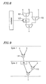
- the circuit of Figure 8 includes: a multiplier 101 for multiplying inputs a and b together; a multiplier 102 for multiplying inputs b and c together; a register (R1) 103 for storing and retaining a multiplication result of the multiplier 101; an adder for adding an output of the register 103 and a multiplication result of the multiplier 102 together so as to output an operation result x; and a controller for generating a signal to control the register 103 .
- the circuit of Figure 8 requires two multipliers, but a selector, which is required in the arithmetic device allocation result shown in Figure 7 , is not required. Therefore, in the case where an area of a multiplier is smaller than that of a selector, the arithmetic device allocation result shown in Figure 8 allows the entire circuit area to be small as compared to the arithmetic device allocation result shown in Figure 7 . On the other hand, in the case where the area of the selector is smaller than that of the multiplier, the arithmetic device allocation result shown in Figure 7 allows the entire circuit area to be small as compared to the arithmetic device allocation result shown in Figure 8 .
- a multiplier has an area larger than that of a selector, and therefore in many cases, the arithmetic device allocation result shown in Figure 7 is preferable.
- an arithmetic device allocation result in which an arithmetic device is not shared between arithmetic operations allows the entire circuit area to be small as compared to the arithmetic device allocation result shown in Figure 7 .
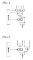
- the circuit shown in Figure 10 includes: a selector for selecting either inputs a or c; a selector for selecting either inputs b or d; an adder for adding the selection results of both selectors together; a register for storing and retaining the addition result of the adder; a multiplier for multiplying an output of the register and the addition result of the adder together so as to output a multiplication result x; and a controller for generating signals to respectively control the register and the selectors.
- the circuit shown in Figure 11 includes: an adder for adding inputs a and b together; a register for storing and retaining the addition result (a + b); an adder for adding inputs c and d together; a multiplier for multiplying the addition result (c + d) and an output of the register together so as to output a multiplication result x; and a controller for generating a signal to control the register.
- the circuit of Figure 10 realizes the additions 111 and 112 using a single adder, but two selectors are required.
- the circuit of Figure 11 requires realizes the additions 111 and 112 using two adders, but no selector is required. Therefore, when the total area of two selectors is smaller than the area of an adder, the arithmetic device allocation result shown in Figure 10 in which the additions 111 and 112 are realized by the single adder allows the entire circuit area to be small as compared to the arithmetic device allocation result shown in Figure 11 .
- an area of an adder is about twice as large as that of a selector having the same bit width as that of the adder, and therefore by using a selector so as to share an adder between additions, rather than separately allocating the additions to adders, the entire circuit area is made small.
- an arithmetic device an adder, a multiplier, or the like
- the entire circuit area is naturally made small.
- the entire circuit area is made small by using a separate adder for each addition so as to reduce the number of selectors, rather than sharing an adder between additions.
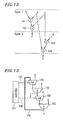
- the circuit shown in Figure 13 includes selectors 154 and 155, an adder 152, a multiplier 153 and a controller 151.
- the additions 141 and 144 are allocated to a single adder 152, and the multiplications 142 and 143 are allocated to a single multiplier 153.
- control signals 157 and 158 output by the controller 151 respectively correspond to 1 and 0. Therefore, the selector 154 selects input a so as to be input to the adder 152.
- the adder 152 calculates an addition (a + b) so as to output the addition result to the selector 155.
- the selector 155 selects the result of the addition (a + b) so as to be input to the multiplier 153.
- the multiplier 153 calculates a multiplication ((a + b) ⁇ c) so as to output a multiplication result x .
- the control signals 157 and 158 output by the controller 151 respectively correspond to 0 and 1.
- the selector 155 selects input d so as to be input to the multiplier 153.
- the multiplier 153 calculates a multiplication (d ⁇ c) so as to output the multiplication result to the selector 154.
- the selector 154 selects the result of the multiplication (d ⁇ c) so as to be input to the adder 152.
- the adder 152 calculates an addition ((d ⁇ c) + b) so as to output an addition result y. In this manner, the circuit of Figure 13 can obtain the operation of the arithmetic operation results x and y shown in Figure 12 using a single adder and a single multiplier.
- the combination circuit refers to a logic circuit in which a logic output thereof is determined by each logic input, and examples of the combination circuit include inverters, NAND circuits, NOR circuits or the like, and a combination thereof.
- a sequential circuit such as a flip flop or a latch circuit, is not included in the combination circuit.
- the control signals 157 and 158 output by the controller 151 do not correspond to 0 simultaneously, and therefore the selectors 154 and 155 do not select a left-side input simultaneously, whereby the loop 156 is unlikely to be activated.
- timings at which the control signals 157 and 158 output by the controller 151 vary can differ from each other, and therefore the loop 156 is activated only for a short period of time.
- the delay for an operation of an adder is 5 ns
- the delay for an operation of each of a multiplier and a divider is 60 ns
- the delay for an operation of a selector is 1 ns
- a clock period is 100 ns.
- the multiplication and the addition are successively performed, and therefore a period of 65 ns is required.
- the clock period is 100 ns, and therefore there is a sufficient amount of time to complete these arithmetic operations.
- the circuit shown in Figure 15 includes: a multiplier 171 ; a selector 174 ; an adder 172 ; a divider 173 ; and a controller 175, and two additions 161 and 162 ( Figure 14 ) are allocated to a single adder 172.
- a control signal 177 output by the controller 175 corresponds to 0. Therefore, the selector 174 selects an output (a ⁇ b) of the multiplier 171 so as to be input to the adder 172.
- the adder 172 adds the output (a ⁇ b) and input c together so as to output an arithmetic operation result x.
- the arithmetic operation result x is correctly output.
- the path from input a to the arithmetic operation result x extends through the multiplier 171 , the selector 174 and the adder 172 , and therefore the delay in that path is 66 ns. Further, the respective delays in the paths from inputs b and c to x are 66 ns and 5 ns, and therefore each of the delays in all the paths is equal to or less than the clock period.
- the control signal 177 output by the controller 175 corresponds to 1. Therefore, the adder 172 receives input d and calculates an addition (d + c) so as to output the addition result to the divider 173.
- the divider 173 calculates a division (d + c)/e so as to output an arithmetic operation result y.
- the arithmetic operation result y is correctly output.
- the path from input d to the arithmetic operation result y extends through the selector 174 , the adder 172 and the divider 173 , and therefore the delay in that path is 66 ns.
- the respective delays in the paths from inputs c and e to the arithmetic operation result y are 65 ns and 60 ns, and therefore each of the delays in all the paths is equal to or less than the clock period.
- the path 176 there is a path 176 from input a to the arithmetic operation result y indicated by the bold line.
- the path 176 extends through the multiplier 171 , the selector 174 , the adder 172 and the divider 173 , and therefore the sum of the delays is 126 ns. If data flows through the path 176 , a delay in the entire circuit becomes greater than the clock period of 100 ns, and therefore circuit malfunction is caused.
- the selector 174 selects data so as to flow through the path from input a to the arithmetic operation result x
- the selector 174 selects data so as to flow through the path from input d to the arithmetic operation result y, and therefore data does not flow through the path from input a to the arithmetic operation result y.
- a path such as the path 176 is referred to as a "false path”.
- a path is a false path or a path through which data actually flows using an automatic logic synthesis tool, a floor planning tool, a layout routing tool, or the like which are presently available. Therefore, a pseudo-timing error is caused because of the generation of a false path longer than a clock period, or an arithmetic device on the false path is replaced by an arithmetic device, which is fast but has a large area, at the time of the optimization in a logic synthesis step, so that a circuit area is increased for no reason. If any tool capable of recognizing the false path is realized in the future, such problems would not be caused, but these problems are frequently caused at present.
- an arithmetic device allocation design method for allocating arithmetic operations in a data flow graph, which includes a branch and a node respectively representing a flow of data and an arithmetic operation, to an arithmetic device based on a scheduling result when performing high-level synthesis for synthesizing a circuit from behavioral descriptions which do not include information about hardware structures and only include a processing algorithm, and the method includes the steps of: in the case of allocating an arithmetic operation A to the arithmetic device, comparing an increased circuit area due to a selector to be provided so as to allocate the arithmetic operation A to an arithmetic device C to which another arithmetic operation B has already been allocated and an increased area due to an arithmetic device D to be created anew to which only the arithmetic operation A is allocated; when the increased circuit area due to the selector is smaller, allocating the arithmetic operation A to the a
- a chip size is made to be as small as possible. Further, in order to realize fast arithmetic operations, by sharing all the arithmetic devices and registers, which are available for sharing, between corresponding arithmetic operations, arithmetic device and register allocations can be performed so as to minimize the number of arithmetic devices and registers, and scheduling can be performed so as to allocate as many arithmetic devices as possible in one clock period.
- Embodiment 1 of the present invention it is possible to obtain an arithmetic device allocation result which results in the total area of an arithmetic device and a selector which is small, so as not to cause an increase in the entire area of a circuit due to employment of a small number of arithmetic devices and a large number of selectors or employment of a large number of arithmetic devices for reducing the number of selectors.
- an arithmetic device allocation design method for allocating arithmetic operations in a data flow graph, which includes a branch and a node respectively representing a flow of data and an arithmetic operation, to an arithmetic device based on a scheduling result when performing high-level synthesis for synthesizing a circuit from behavioral descriptions which do not include information about hardware structures and only include only processing algorithm, and the method includes the steps of: in the case of allocating a plurality of arithmetic operations to a single arithmetic device, determining whether or not a loop extending through only a combination circuit is generated; when a loop extending through only a combination circuit is not generated, allocating the plurality of arithmetic operations to the arithmetic device; and when a loop extending through only a combination circuit is generated, separately allocating the plurality of arithmetic operations to different arithmetic devices.
- Embodiment 2 of the present invention it is possible to obtain an arithmetic device allocation result so as to prevent the generation of a loop extending through only a combination circuit, and therefore it is possible to prevent an increase in power consumption due to oscillation of the circuit and/or circuit malfunction. Further, it is possible to precisely estimate the delays in the steps of logic synthesis, floor planning, routing of layout, etc.
- the presence of the loop can be detected by determining whether or not the same arithmetic operation as a focused arithmetic operation is present as a pre- or post-arithmetic operation. When the same arithmetic operation as the focused arithmetic operation is present, the loop is determined to be present.
- an arithmetic device allocation design method for allocating arithmetic operations in a data flow graph, which includes a branch and a node respectively representing a flow of data and an arithmetic operation, to an arithmetic device based on a scheduling result when performing high-level synthesis for synthesizing a circuit from behavioral descriptions which do not include information about hardware structures and only include only processing algorithm, and the method includes the steps of: in the case of allocating a plurality of arithmetic operations to a single arithmetic device, determining whether or not a false path longer than a designated period of time is generated; when a false path longer than a designated period of time is not generated, allocating the plurality of arithmetic operations to the arithmetic device; and when a false path longer than a designated period of time is generated, separately allocating the plurality of arithmetic operations to different arithmetic devices.
- a false path is a path on which no operation can be actually performed in terms of the operation of the LSI circuit, and therefore no problems are caused in the actual LSI circuit itself if a false circuit is present in the circuit.
- the conventional design verification tool and the conventional logic synthesis tool cannot recognize a false path, and therefore problems are caused.
- the design verification tool recognizes the delay greater than a clock period as an error. Further, the conventional logic synthesis tool mistakenly recognizes a false path as a path on which any operation is actually performed, and thus the false path is optimized.
- the circuit is required to be designed such that each operation performed in the paths which are present between one register and another register is completed within a delay of a clock period, and therefore when the delay caused by the presence of the false path is greater than a clock period, the optimization operation is performed by replacing an arithmetic device(s) on the false path with a faster arithmetic device(s) such that the delay caused by the false path is within one clock period.
- a fast arithmetic device has a large area, and therefore the circuit area is increased. Further, no operation is actually performed on the false path, and therefore such an optimization operation is unnecessary and the circuit area is increased for no reason.
- a clock period ⁇ ⁇ is set as a designated value.
- the circuit design is performed again so as to reperform arithmetic device allocation.
- a false path temporally shorter than a clock period ⁇ ⁇ is present, originally performed arithmetic device allocation is employed. The reason for this is that the false path is a path on which no operation is actually performed, and therefore no problems are caused in the LSI circuit. Further, in this case, no error is caused even in the case of using the design verification tool, and therefore no problems are caused in terms of circuit operations.
- Embodiment 3 of the present invention it is possible to obtain an arithmetic device allocation result which does not generate a false path equal to or longer than a designated period, and therefore it is possible to prevent the generation of a pseudo-timing error caused to a false path longer than a clock period and/or a circuit area from being increased for no reason due to the replacement of an arithmetic device on a false path by another arithmetic device, which is fast but has a large area, at the time of the optimization in a logic synthesis step.
- the arithmetic operation allocation is sequentially performed from an arithmetic operation using an arithmetic device having a large area.
- the invention described herein makes possible the advantages of providing an arithmetic device allocation design method capable of reducing circuit scale so as not to include a loop including only a combination circuit and a long false path in the circuit.
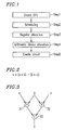
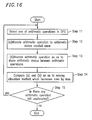
- FIG 16 is a flowchart for explaining an arithmetic device allocation design method according to Embodiment 1 of the present invention.
- arithmetic operations in a data flow graph (DFG) are allocated to corresponding arithmetic devices one by one based on a scheduling result.
- DFG data flow graph
- one of the arithmetic operations in the DFG is selected.
- the following two methods (a) and (b) are respectively attempted at steps 12 and 13: (a) the arithmetic operation selected at step 11 is allocated to an arithmetic device created anew; and (b) an arithmetic operation is allocated to an arithmetic device to which another arithmetic operation has already been allocated so as to share the arithmetic device between these arithmetic operations.
- a selector is provided so as to prevent the arithmetic operations from interfering with each other. Further, in the case where there are a plurality of arithmetic devices on which an allocation operation can be performed according to the method (b), the allocation operation is attempted with respect to each of the plurality of arithmetic devices.
- step 14 comparison between an increased area of the arithmetic device created anew when the arithmetic operation is allocated to the arithmetic device according to the method (a) and an increased area of the selector provided when the arithmetic operation is allocated to the arithmetic device according to the method (b) is made, and an allocation method which increases the area by less is employed.
- an allocation operation resulting in the smallest circuit area is employed as the method (b).
- step 15 it is determined whether or not there is an arithmetic operation(s) left unallocated. If there is an arithmetic operation(s) left unallocated, the process returns to step 11, and when there is no arithmetic operation left unallocated, the process is ended.
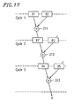
- Embodiment 1 The arithmetic device allocation design method according to Embodiment 1 is described in detail below in conjunction with a case where the arithmetic operations in the DFG are allocated to the arithmetic devices based on the scheduling and register allocation results shown in Figure 17 . In this case, areas of an adder and a selector are respectively represented by 9 and 5.
- the addition 211 is allocated to an arithmetic device created anew based on the scheduling and register allocation results shown in Figure 17 according to the method (a), so that an allocation result denoted by reference numeral 221 in Figure 18 is obtained.
- a circuit area is 9 which corresponds to one adder.
- the method (b) for sharing an arithmetic device with another arithmetic operation is not performed.
- the addition 212 is allocated to an arithmetic device created anew according to the method (a) so that an allocation result denoted by reference numeral 222 in Figure 18 is obtained.
- a circuit area is 18 which corresponds to two adders.
- a circuit area is 14 which corresponds to one adder and one selector.
- a circuit area is 23 which corresponds to two adders and one selector.
- the addition 213 is allocated to the arithmetic device of the allocation result 223 according to the method (b) for sharing an arithmetic device with another arithmetic operation so that an allocation result denoted by reference numeral 225 in Figure 18 is obtained.
- a circuit area is 24 which corresponds to one adder and three selectors.
- the arithmetic device allocation described above results in the circuit shown in Figure 19.
- the circuit of Figure 19 includes: registers R1-R5; a selector for selecting one of outputs of the registers R2 and R3; an adder for adding outputs of the register R1 and the selector together so as to output the addition result to the registers R1 or R4; an adder for adding outputs of the registers R1 and R4 so as to output an operation result x; and a controller for generating signals to respectively control the registers R1-R5 and the selector.
- the circuit shown in Figure 21 includes: registers R1-R5; a (left-side) selector for selecting one of outputs of the registers R1 and R4; a (right-side) selector for selecting one of outputs of the registers R3 and R5 ; a (middle) selector for selecting one of outputs of the register R2 and the right-side selector; an adder for adding outputs of the left-side and middle selectors so as to input the addition result to the registers R1 or R4 or to output an operation result x; and a controller for generating signals to respectively control the registers R1-R5 and the selectors.
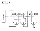
- Figure 22 shows an arithmetic device allocation result in the case where arithmetic devices are not shared between any operations, and the circuit to be created in this case is as shown in Figure 23 .
- the circuit of Figure 23 includes: registers R1-R5, an adder for adding outputs of the registers R1 and R2 so as to output the addition result to the register R1; an adder for adding outputs of the registers R1 and R3 so as to output the addition result to the register R4; an adder for adding outputs of the registers R4 and R5 so as to output an operation result x; and a controller for generating signals to respectively control the registers R1-R5 .
- Embodiment 1 by comparing an increased area of an arithmetic device created anew and an increased area of a selector provided for sharing an arithmetic device between arithmetic operations so as to select an optimum arithmetic device allocation method, it is possible to obtain an arithmetic device allocation operation resulting in a small circuit area. Therefore, it is possible to perform arithmetic device allocation which can realize a highly-integrated LSI based on a scheduling result which improves a speed in an arithmetic operation.
- Figure 24 is a flowchart for explaining an arithmetic device allocation design method according to Embodiment 2.
- Embodiment 2 prevents the loop including only a combination circuit as shown in Figure 13 from being generated when an arithmetic operation in the DFG is allocated to an arithmetic device based on a scheduling result.
- a preparatory step data dependency between arithmetic operations is examined according to a procedure as follows.
- all the arithmetic operations to be allocated to arithmetic devices are detected from the DFG based on scheduling and register allocation results so as to be listed as focused arithmetic operations.
- each arithmetic device 141-144 is listed as a focused arithmetic operation based on, for example, the scheduling result of Figure 12.
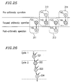
- a pre-arithmetic operation or a post-arithmetic operation is determined with respect to each focused arithmetic operation.
- the pre-arithmetic operation refers to an arithmetic operation which is performed in the same clock cycle as its associated focused arithmetic operation and provides data to the associated focused arithmetic operation.
- the pre-arithmetic operation of the focused arithmetic operation 142 is the arithmetic device 141 and the pre-arithmetic operation of the focused arithmetic operation 144 is the arithmetic device 143.
- the post-arithmetic operation refers to an arithmetic operation which is performed in the same clock cycle as its associated focused arithmetic operation and receives data from the associated focused arithmetic operation.
- the post-arithmetic operation of the focused arithmetic operation 141 is the arithmetic device 142 and the post-arithmetic operation of the focused arithmetic operation 143 is the arithmetic device 144.
- Another operation can be provided between a pre-or post-arithmetic operation and its associated focused arithmetic operation.
- a multiplication 321 is performed in cycle 1 and multiplications 322-324 are performed in cycle 2
- the multiplication 322 is determined as a focused arithmetic operation
- the multiplication 324 are post-arithmetic operations.
- an arithmetic operation such as the operation 321 which is performed in a different cycle is not included in the pre- or post-arithmetic operations.
- step 23 of Figure 24 a loop is detected according to the following procedure.
- a case where arithmetic device allocation is performed on arithmetic operations in the DFG based on the scheduling result shown in Figure 12 is described as an example.
- the loop including only a combination circuit is generated only in the case where each of two or more arithmetic devices is shared between corresponding two or more operations. Therefore, the loop is not generated by merely allocating the multiplications 142 and 143 to the single multiplier.
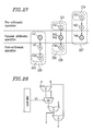
- the multiplications 142 and 143 are combined together according to the following procedure so as to change the focused arithmetic operations, pre-arithmetic operations and post-arithmetic operations as shown in Figure 27 .
- arithmetic operation units 312 and 313 shown in Figure 25 including the multiplications 142 and 143 as their respective focused arithmetic operations are combined as a single arithmetic operation unit 335 shown in Figure 27 .
- the pre-arithmetic operation 141 of the operation unit 312 and the post-arithmetic operation 144 of the arithmetic operation unit 313 are connected in parallel to each other.
- the arithmetic operation unit 312 includes only the pre-arithmetic operation of the arithmetic operation 142, and the arithmetic operation unit 313 includes only the post-arithmetic operation of the arithmetic operation 143 , and therefore the pre- and post-arithmetic operations of the arithmetic operation unit 335 shown in Figure 27 respectively correspond to arithmetic operations 331 and 332.
- arithmetic operation units 311 and 314 shown in Figure 25 including the multiplications 142 and 143 , which are combined together as a single multiplication, as a pre- or post-arithmetic operation are renewed so as to be arithmetic operational units 336 or 337 , respectively, as shown in Figure 27 .
- a post-arithmetic operation 332 newly added to the arithmetic operation unit 335 of Figure 27 is further added to the arithmetic operation unit 336 as a post-arithmetic operation 333 .
- a pre-arithmetic operation 331 newly added to the arithmetic operation unit 335 of Figure 27 is further added to the arithmetic operation unit 337 as a pre-arithmetic operation 334.
- the condition that the loop including only a combination circuit is generated is as follows.
- the operation B when the operation B is a focused arithmetic operation, the operation C is a pre- or post-arithmetic operation of the operation B, or when the operation C is a focused arithmetic operation, the operation B is a pre- or post-arithmetic operation of the arithmetic operation C.
- additions 141 and 144 are allocated to a single adder, in Figure 27 , when the addition 141 is a focused arithmetic operation, post-arithmetic operations thereof include the addition 144 , and when the addition 144 is a focused arithmetic operation, pre-arithmetic operations of the addition 144 include the addition 144. Therefore, it is appreciated that the allocation of the additions 141 and 144 to a single arithmetic device results in the loop including only a combination circuit.
- step 23 of Figure 24 it is determined whether or not the loop including only a combination circuit is generated when a plurality of arithmetic operations are allocated to a single arithmetic device using the method described above.
- the process proceeds to step 25 so as to allocate the plurality of arithmetic operations to a single arithmetic device, and at step 26, the pre- and post-arithmetic operations are renewed.
- the process proceeds to step 24 so as to separately allocate the plurality of arithmetic operations to different arithmetic devices.
- the circuit of Figure 28 includes: an adder for adding inputs a and b; a selector for selecting one of an output of the adder and input d so as to output the selection result; a multiplier for multiplying the output of the selector and input c together so as to output the multiplication result to a downstream adder or output an arithmetic operation result x; the downstream adder for adding the output of the multiplier and input b together so as to output an arithmetic operation result y; and a controller for outputting a signal k1 to control the selector.
- the circuit of Figure 28 does not include the loop 156 including only a combination circuit shown in Figure 13 , and therefore there is substantially no possibility that power consumption of a circuit is increased or the operation of the circuit is made unstable due to the oscillation of the circuit.
- step 27 of Figure 24 it is determined whether or not all the arithmetic operations are allocated to their corresponding arithmetic devices. When there is any arithmetic operation left unallocated, the process returns to step 23, and when there is no arithmetic operation left unallocated, the process is ended.
- the arithmetic device allocation design method according to Embodiment 2 can be used in combination with the arithmetic device allocation design method according to Embodiment 1.
- a selection is made between a case where each arithmetic operation is allocated to an arithmetic device to which another arithmetic operation has already been allocated and a case where each arithmetic operation is allocated to an arithmetic device created anew, such that the entire circuit area resulting from the selected case is smaller than that resulting from the other case.
- Whether or not the loop including only a combination circuit is generated is determined by applying the arithmetic device allocation design method according to Embodiment 2 to the case where each arithmetic operation is allocated to an arithmetic device to which another operation has been allocated. If the loop including only a combination circuit is generated, the allocation method is not performed and each arithmetic operation is allocated to an arithmetic device created anew, thereby preventing the generation of the loop including only a combination circuit.
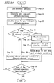
- Figure 31 is a flow chart for explaining an arithmetic device allocation design method according to Embodiment 3.
- a false path refers to a path on which no operation is actually performed, and therefore no problems are caused to a circuit itself if the false circuit is present in the circuit.
- a conventional design verification tool cannot determine whether a path is a false path or a path on which any operation is actually performed, and thus detects the false path only as an error, thereby causing problems.
- Embodiment 3 prevents the generation of the false path causing a delay greater than a designated value when allocating the arithmetic operations to the arithmetic devices.
- step 31 in Figure 31 all the arithmetic operations to be allocated to an arithmetic device are detected from the DFG based on scheduling and register allocation results so as to be listed as focused arithmetic operations.
- step 32 a pre- or post-arithmetic operation is determined with respect to each focused arithmetic operation.
- the steps 31 and 32 can be performed in a similar manner to steps 21 and 22 shown in Figure 24 .
- step 33 respective delay times of the focused arithmetic operations and pre- and post arithmetic operations are calculated.
- a delay time required to complete all the arithmetic operations is calculated.
- the arithmetic operations A and B are the same as each other, and therefore the respective delay times are the same as each other.
- the delay in the false path and a designated value are compared, and when the delay in the false path is greater than the designated value, the false path is generated so as to cause a delay greater than the designated value.
- a case where arithmetic operations in the DFG are allocated to arithmetic devices based on a scheduling result shown in Figure 32 is described as an example.
- the delay for an operation of a multiplier is 60 ns
- the delay for an operation of an adder is 5 ns
- the delay for an operation of a selector is 1 ns
- a clock period is 100 ns.
- the associated pre- or post-arithmetic operations of focused arithmetic operations 411-414 of the DFG shown in Figure 32 are as shown in Figure 33.
- Delay times of the focused arithmetic operations 411-414 and their associated pre- and post-arithmetic operations are as shown in Table 1.
- Focused nodes 411 412 413 414 Delay for PRAO 0 60 0 5
- Delay for POAO 5 0 60 0 *"PRAO", "FAO", and "POAO” respectively denote "pre-arithmetic operation", “Focused arithmetic operation", and "Post-arithmetic operation".
- the delay of the multiplication 411 is 60 ns and the delays of the pre- and post-operations thereof are 0 ns and 5 ns, respectively.
- the delay in the false path of 70 ns is less than the designated value 100 ns, and therefore the false path generated by allocating the multiplications 411 and 414 to a single multiplier does not prevent the optimization in a logic synthesis step.
- the false path if present, causes no problem since it is not generated as a data path in an actual circuit.
- the design verification tool detects the false path as an error so that arithmetic device allocation is required to be performed again.
- a circuit obtained by allocating the multiplications 411 and 414 to a single multiplier and separately allocating additions 412 and 413 to different adders based on the scheduling result shown in Figure 32 is shown in Figure 34 .
- the circuit of Figure 34 includes: an adder for adding inputs d and c together; a selector for selecting one of an output of the adder and input a; a multiplier for multiplying an output of the selector and input b together so as to output the multiplication result to a downstream adder or output an arithmetic operation result y; the downstream adder for adding the output of the multiplier and input c so as to output an arithmetic operation result x; and a controller for creating a signal k1 to control the selector.
- a path 441 from input d to the arithmetic operation result x indicated by the bold line is a false path.
- the path 441 extends through the adder, the selector, the multiplier and the downstream adder, and therefore the sum of delays is 71 ns which is less than the designated value 100 ns corresponding to the clock period.
- Embodiment 3 when estimating the delay in the false path using the delays for the focused operations, and the delays for the pre- and post-operations as shown in Table 1, the delay for an operation of the selector (about 1 ns to 2 ns) is not considered, and therefore in consideration of the delay for an operation of the selector as a margin, a value slightly less than the clock period, e.g., 95 ns, can be designated as the value to be compared with the delay in the false path.
- a value slightly greater than the clock period e.g., 120 ns, can be designated as the value to be compared with the delay in the false path while allowing the generation of the false path causing a delay slightly longer than the clock period.
- the delay for the addition 412 is 5 ns, and the delays of the pre- and post-arithmetic operations thereof are 60 ns and 0 ns, respectively.
- the delay in false path of 125 ns is greater than the designated value 100 ns, and therefore there is a possibility that the false path generated by allocating the additions 412 and 413 to a single adder might be detected as a timing error by a design verification tool in a logic synthesis step.
- the delay in the false path is optimized so as to be equal to or less than 100 ns by using the logic synthesis tool to replace an arithmetic device on the false path with another arithmetic device which is operated at a high speed but has a larger area.
- the path is a false path, and therefore such optimization is not necessary. This merely increases the circuit area.
- a circuit obtained by allocating the additions 412 and 413 to a single adder and separately allocating the multiplications 411 and 414 to different arithmetic devices based on the scheduling result shown in Figure 32 is shown in Figure 35.
- the circuit of Figure 35 includes : a multiplier for multiplying inputs a and b together; a selector for selecting one of an output of the multiplier and input d; an adder for adding an output of the selector and input c together so as to output the addition result to a downstream multiplier or output an arithmetic operation result x; the downstream multiplier for multiplying the output of the adder and input b so as to output an arithmetic operation result y; and a controller for creating a signal k1 to control the selector.
- a path 451 from input a to the arithmetic operation result y indicated the bold line is the false path.
- the path 451 extends through the multiplier, the selector, the adder and the downstream multiplier, and therefore the sum of delays is 126 ns which is greater than the designated value 100 ns corresponding to the clock period.
- Embodiment 3 when the arithmetic device allocation is performed based on the scheduling result shown in Figure 32 , even if the multiplications 411 and 414 are allocated to a single multiplier, a false path longer than the clock period is not generated. However, it is possible to easily detect that a false path longer than the clock period is generated by allocating the additions 412 and 413 to a single adder.
- step 34 of Figure 31 when the false path longer than the clock period is generated as in the case where the additions 412 and 413 are allocated to a single adder, the process proceeds to step 35 so as to separately allocate the plurality of arithmetic operations (additions 412 and 413 ) to different arithmetic devices.
- step 36 in the case where the false path longer than the clock period is not generated as in the case where the multiplications 411 and 414 are allocated to a single multiplier, the process proceeds to step 36 so as to allocate the plurality of arithmetic operations to a single arithmetic device and at step 37, the pre- and post-arithmetic operations of the plurality of arithmetic operations are renewed.
- step 38 the delays of the pre- and post-operations are renewed correspondingly. Therefore, it is possible to prevent the generation of the false path longer than the clock period.
- step 39 it is determined whether or not all the arithmetic operations have been allocated to their corresponding arithmetic devices. When there is an arithmetic operation(s) left unallocated, the process proceeds to step 34, and when there is no operation to be allocated, the process is ended.
- Each arithmetic operation included in the DFG of Figure 36 is a monadic arithmetic device to which only one input is provided.
- a circle including "r" therein denotes a round-off arithmetic operation and the delay for the round-off arithmetic operation is 10 ns.
- Circles each including "+1" therein denote increment arithmetic operations and the delay for each increment arithmetic operation is 10 ns.
- Circles each including " ⁇ 2" therein denote squaring arithmetic operations and the delay for each squaring arithmetic operation is 65 ns.
- a circle including " ⁇ 2" therein denotes a double arithmetic operation and the delay for the double arithmetic operation is 10 ns.
- the clockperiod is 100 ns.
- each of the arithmetic operations 462 , 463, 464, 465 and 466 can share a single arithmetic device with another arithmetic operation.
- pre- and post-operations associated with the focused arithmetic operations are as shown in Figure 37.
- Delay times of the focused arithmetic operations shown in Figure 37 and their associated pre- and post- arithmetic operations are as shown in Table 2. Focused nodes 462 463 464 465 466 Delay for PRAO 10 0 10 10 0 Delay for FAO 10 10 10 65 65 Delay for POAO 0 75 65 0 10
- the arithmetic operations 463 and 464 are performed in the same clock cycle, i.e., clock cycle 2, and therefore cannot not be allocated so as to share a single arithmetic device between them.
- arithmetic operations performed in different cycles can share a single arithmetic device, and therefore arithmetic operations 462 and 463, arithmetic operations 462 and 464, and arithmetic operations 465 and 466 are possible combinations for sharing a single arithmetic device.
- the delays of these combinations of the arithmetic operations are estimated to be 95 ns (arithmetic operations 462 and 463 ), 85 ns (arithmetic operations 462 and 464 ) and 85 ns (arithmetic operations 465 and 466 ) , respectively. Therefore, it is appreciated that when a single arithmetic device is shared by any one of these combinations of the arithmetic operations, a false path exceeding the clock cycle of 100 ns cannot be generated.
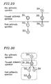
- the arithmetic operation 465 of an arithmetic operation unit 474 and the arithmetic operation 466 of an arithmetic operation unit 475 which are shown in Figure 37 are combined together as an arithmetic operation unit 494 shown in Figure 38.
- the pre-arithmetic operations 463 and 464 in the arithmetic operation unit 474 and the post-arithmetic operation 467 in the operation unit 475 which are shown in Figure 37 are connected in parallel to each other.
- the arithmetic operation unit 474 does not have any post-arithmetic operation and the operation unit 475 does not have any pre-arithmetic operation, and therefore the pre-arithmetic operation and post-arithmetic operation in the arithmetic operation unit 494 are respectively as denoted by reference numerals 481 and 482.
- the post-arithmetic operation 482 in an arithmetic operation unit 494 shown in Figure 38 is added to each of arithmetic operation units 472 and 473 shown in Figure 37 each including the arithmetic operation 465 as a post-arithmetic operation so that a post-arithmetic operation 483 in an arithmetic operation unit 492 and a post-arithmetic operation 484 in a arithmetic operation unit 493 are provided.
- Table 2 representing the delays for the pre-and post-arithmetic operations is renewed as Table 3 according to the delays for the pre- and post-arithmetic operations shown in Figure 38.
- Focused node 462 463 464 (465, 466) Delay for PRAO 10 0 10 20 Delay for FAO 10 10 10 65 Delay for POAO 0 85 75 10
- the lengths of false paths (delays in false paths) generated when separately allocating the combination of the arithmetic operations 462 and 463 and the combination of the arithmetic operations 462 and 464 to their respective common arithmetic devices are estimated again using expression (1).
- the estimated delays in these false paths are 105 ns and 95 ns, respectively. From this estimation, it is appreciated that when the arithmetic operations 462 and 463 are allocated to a single arithmetic device, a false path longer than the clock period of 100 ns is generated, and when the arithmetic operations 462 and 464 are allocated to a single arithmetic device, a false path longer than the clock period of 100 ns is not generated.
- Embodiment 3 in the estimation performed before allocating the arithmetic operations 465 and 466 to a single arithmetic device, it is detected that even if the arithmetic operations 462 and 463 are allocated to a single arithmetic device, a false path longer than the clock period of 100 ns is not generated. However, in the estimation performed after allocating the arithmetic operations 465 and 466 to a single arithmetic device, it is detected that a false path longer than the clock period of 100 ns is created due to the influence of the allocation of the arithmetic operations 465 and 466.
- FIG. 39 A circuit obtained by allocating the arithmetic operations 465 and 466 to a single arithmetic device and further allocating the operations 462 and 464 to a single arithmetic device based on the scheduling result shown in Figure 36 is shown in Figure 39.
- the circuit of Figure 39 includes: a round-off arithmetic device for rounding off input a to the nearest whole number; an adder for incrementing input b by one; a selector for selecting one of outputs of the round-off arithmetic device and the adder; an adder 532 for incrementing an output of the selector by one so as to output the increment result to a downstream selector or to output an arithmetic operation result x; the downstream selector for selecting one of the output of the adder 532 and input c; a square arithmetic device 531 for squaring the output of the downstream selector so as to output the squared result to a double arithmetic device or to output an arithmetic operation result y; the double arithmetic device for doubling the output of the square arithmetic device 531 so as to provide output z; and a controller for creating a signal to control the selector.
- the arithmetic device 531 performs the arithmetic operations 465 and 466 ( Figure 36 ), and the arithmetic device 532 performs the arithmetic operations 462 and 464 ( Figure 36 ).
- the longest false path included in the circuit of Figure 39 is a path 533 from input a to output z indicated by the bold line.
- the path 533 extends through the round-off arithmetic device, the adder, the square arithmetic device, the double arithmetic device and two selectors.
- the delay for an operation of the selector is 1 ns
- the arithmetic device allocation design method according to Embodiment 3 can be used in combination with the arithmetic device allocation design method according to Embodiment 1.
- a selection is made between a case where each arithmetic operation is allocated to an arithmetic device to which another arithmetic operation has already been allocated and a case where each arithmetic operation is allocated to an arithmetic device created anew, such that the entire circuit area resulting from the selected case is smaller than that resulting from the other case.
- Whether or not a false path greater than a designated value is generated is determined by applying the arithmetic device allocation design method according to Embodiment 3 to the case where each arithmetic operation is allocated to an arithmetic device to which another operation has been allocated. If a false path greater than the designated value is generated, the allocation method is not performed and each operation is allocated to an arithmetic device created anew, thereby preventing the generation of a false path greater than the designated value.
- Embodiment 4 of the present invention is described with respect to a method for sequentially allocating arithmetic operations in the DFG to arithmetic devices based on a scheduling result in which the arithmetic device allocation is performed so as to begin with an arithmetic operation using an arithmetic device having a large area and end with an arithmetic operation using an arithmetic device having a small area.
- circuits of Figures 28 and 40 perform similar processes. However, the circuit of Figure 28 includes two adders and one multiplier while the circuit of Figure 40 includes one adder and two multipliers. In general, an area of a multiplier is more than several times the area of an adder, and therefore the circuit of Figure 40 has a larger area than the circuit of Figure 28.
- the arithmetic device allocation is sequentially performed from an arithmetic operation using an arithmetic device having a large area, and therefore allocation of arithmetic operations to arithmetic devices having a small area is performed after allocating the arithmetic operation using the arithmetic device having a large area. Therefore, in order to prevent the generation of the loop including only a combination circuit using the method according to Embodiment 2, a plurality of arithmetic operations are separately allocated to arithmetic devices having a large area and another plurality of arithmetic operations are separately allocated to a plurality of arithmetic devices having a small area.
- the arithmetic device allocation performed based on the scheduling result shown in Figure 12 results in the circuit of Figure 28 but does not result in the circuit of Figure 40.
- the arithmetic device allocation design method of Embodiment 4 can be used in combination with the arithmetic device allocation method of Embodiment 3.
- the arithmetic device allocation design method according to Embodiment 3 in the case of allocating a plurality of arithmetic operations to a single arithmetic device and then allocating another plurality of arithmetic operations to another single arithmetic device, when it is determined that a false path greater than a designated value is generated, arithmetic operations are separately allocated to different arithmetic devices rather than sharing one arithmetic device between the arithmetic operations.
- the arithmetic device allocation design method according to Embodiment 4 is applied so as to sequentially perform arithmetic device allocation from an arithmetic operation using an arithmetic devices having a large area.
- This increases arithmetic devices having a relatively small area even in the case where arithmetic operations are separately allocated to different arithmetic devices, rather than sharing the arithmetic device between the arithmetic operations, so as to prevent the generation of a false path greater than a designated value. Therefore, it is possible to minimize an increase in circuit area, thereby obtaining a circuit having a small area.
- an arithmetic device allocation result which makes the total area of an arithmetic device and a selector to be small, so as not to cause an increase in the entire area of a circuit due to employment of a small number of arithmetic devices and a large number of selectors or employment of a large number of arithmetic devices for reducing the number of selectors.
- the present invention it is possible to prevent the generation of the loop extending through only a combination circuit, and therefore it is possible to prevent an increase of power consumption due to oscillation of the circuit or to prevent circuit malfunction. Furthermore, it is possible to precisely estimate the delays in the steps of logic synthesis, floor planning, routing of layout, etc.
Landscapes
- Engineering & Computer Science (AREA)
- Computer Hardware Design (AREA)
- Physics & Mathematics (AREA)
- Theoretical Computer Science (AREA)
- Evolutionary Computation (AREA)
- Geometry (AREA)
- General Engineering & Computer Science (AREA)
- General Physics & Mathematics (AREA)
- Design And Manufacture Of Integrated Circuits (AREA)
- Complex Calculations (AREA)
Abstract
Description
| | 411 | 412 | 413 | 414 |
| Delay for PRAO | 0 | 60 | 0 | 5 |
| Delay for FAO | 60 | 5 | 5 | 60 |
| Delay for POAO | 5 | 0 | 60 | 0 |
| *"PRAO", "FAO", and "POAO" respectively denote "pre-arithmetic operation", "Focused arithmetic operation", and "Post-arithmetic operation". |
| | 462 | 463 | 464 | 465 | 466 |
| Delay for PRAO | 10 | 0 | 10 | 10 | 0 |
| Delay for FAO | 10 | 10 | 10 | 65 | 65 |
| Delay for POAO | 0 | 75 | 65 | 0 | 10 |
| | 462 | 463 | 464 | (465, 466) |
| Delay for PRAO | 10 | 0 | 10 | 20 |
| Delay for FAO | 10 | 10 | 10 | 65 |
| Delay for POAO | 0 | 85 | 75 | 10 |
Claims (9)
- An arithmetic device allocation design method for allocating arithmetic operations in a data flow graph, which includes a branch and a node respectively representing a flow of data and an arithmetic operation, to an arithmetic device based on a scheduling result when performing high-level synthesis for synthesizing a circuit from behavioral descriptions which do not include information about hardware structures and only include a processing algorithm, the method comprising the steps of:in the case of allocating an arithmetic operation A to the arithmetic device, comparing an increased circuit area due to a selector to be provided so as to allocate the arithmetic operation A to an arithmetic device C to which another arithmetic operation B has already been allocated and an increased area due to an arithmetic device D to be created anew to which only the arithmetic operation A is allocated;when the increased circuit area due to the selector is smaller, allocating the arithmetic operation A to the arithmetic device C to which the another arithmetic operation B has already been allocated while providing the selector; andwhen the increased circuit area due to the arithmetic device D is smaller, creating the arithmetic device D anew so as to allocate the arithmetic operation A to the arithmetic device D created anew.
- An arithmetic device allocation design method according to claim 1, wherein the arithmetic operation allocation is sequentially performed from an arithmetic operation using an arithmetic device having a large area.
- An arithmetic device allocation design method for allocating arithmetic operations in a data flow graph, which includes a branch and a node respectively representing a flow of data and an arithmetic operation, to an arithmetic device based on a scheduling result when performing high-level synthesis for synthesizing a circuit from behavioral descriptions which do not include information about hardware structures and only include only processing algorithm, the method comprising the steps of:in the case of allocating a plurality of arithmetic operations to a single arithmetic device, determining whether or not a loop extending through only a combination circuit is generated;when a loop extending through only a combination circuit is not generated, allocating the plurality of arithmetic operations to the arithmetic device; andwhen a loop extending through only a combination circuit is generated, separately allocating the plurality of arithmetic operations to different arithmetic devices.
- An arithmetic device allocation design method according to claim 3, wherein the arithmetic operation allocation is sequentially performed from an arithmetic operation using an arithmetic device having a large area.
- An arithmetic device allocation design method for allocating arithmetic operations in a data flow graph, which includes a branch and a node respectively representing a flow of data and an arithmetic operation, to an arithmetic device based on a scheduling result when performing high-level synthesis for synthesizing a circuit from behavioral descriptions which do not include information about hardware structures and only include only processing algorithm, the method comprising the steps of:in the case of allocating a plurality of arithmetic operations to a single arithmetic device, determining whether or not a false path longer than a designated period of time is generated;when a false path longer than a designated period of time is not generated, allocating the plurality of arithmetic operations to the arithmetic device; andwhen a false path longer than a designated period of time is generated, separately allocating the plurality of arithmetic operations to different arithmetic devices.
- An arithmetic device allocation design method according to claim 5, wherein the arithmetic operation allocation is sequentially performed from an arithmetic operation using an arithmetic device having a large area.
- A computer program adapted so as to execute the arithmetic device allocation design method according to any preceding claim when run on computer apparatus.
- A high level synthesis method for synthesizing a circuit from behavioral descriptions constituted by a processing algorithm to be executed by the circuit, said method including an arithmetic device allocation design method according to any of claims 1 to 6, the synthesis method including the step of creating the circuit in accordance with the results of said arithmetic device allocation design method.
- A high level synthesis method according to claim 8, including the step of materially producing the circuit created in accordance with the results of said arithmetic device allocation design method.
Applications Claiming Priority (2)
| Application Number | Priority Date | Filing Date | Title |
|---|---|---|---|
| JP2001264287A JP4029959B2 (en) | 2001-08-31 | 2001-08-31 | Arithmetic unit allocation design apparatus and arithmetic unit allocation design method |
| JP2001264287 | 2001-08-31 |
Publications (2)
| Publication Number | Publication Date |
|---|---|
| EP1288801A2 true EP1288801A2 (en) | 2003-03-05 |
| EP1288801A3 EP1288801A3 (en) | 2005-09-07 |
Family
ID=19090917
Family Applications (1)
| Application Number | Title | Priority Date | Filing Date |
|---|---|---|---|
| EP02256052A Withdrawn EP1288801A3 (en) | 2001-08-31 | 2002-08-30 | Method for designing arithmetic device allocation |
Country Status (3)
| Country | Link |
|---|---|
| US (2) | US6915504B2 (en) |
| EP (1) | EP1288801A3 (en) |
| JP (1) | JP4029959B2 (en) |
Cited By (1)
| Publication number | Priority date | Publication date | Assignee | Title |
|---|---|---|---|---|
| CN103207885A (en) * | 2012-01-16 | 2013-07-17 | 卡西欧计算机株式会社 | Semiconductor Circuit Design Supporting Apparatus And Method, And Non-transitory Computer-readable Medium |
Families Citing this family (9)
| Publication number | Priority date | Publication date | Assignee | Title |
|---|---|---|---|---|
| JP4029959B2 (en) * | 2001-08-31 | 2008-01-09 | シャープ株式会社 | Arithmetic unit allocation design apparatus and arithmetic unit allocation design method |
| US7523434B1 (en) * | 2005-09-23 | 2009-04-21 | Xilinx, Inc. | Interfacing with a dynamically configurable arithmetic unit |
| US8094768B2 (en) * | 2005-12-23 | 2012-01-10 | Triductor Technology (Suzhou) Inc. | Multi-channel timing recovery system |
| JP2007193529A (en) * | 2006-01-18 | 2007-08-02 | Matsushita Electric Ind Co Ltd | Method for high-level synthesis of semiconductor integrated circuit |
| JP2007287044A (en) * | 2006-04-19 | 2007-11-01 | Toshiba Corp | Design support device |
| US8935651B1 (en) * | 2007-12-28 | 2015-01-13 | Cadence Design Systems, Inc. | Methods and apparatus for data path cluster optimization |
| JP5056644B2 (en) * | 2008-07-18 | 2012-10-24 | 富士通セミコンダクター株式会社 | Data conversion apparatus, data conversion method and program |
| JP5842255B2 (en) | 2013-12-12 | 2016-01-13 | 国立大学法人東京工業大学 | Apparatus and method for generating logic circuit from logic circuit description in programming language |
| JP6663801B2 (en) * | 2016-06-15 | 2020-03-13 | 株式会社日立製作所 | Semiconductor LSI design apparatus and design method |
Family Cites Families (16)
| Publication number | Priority date | Publication date | Assignee | Title |
|---|---|---|---|---|
| US5841663A (en) * | 1995-09-14 | 1998-11-24 | Vlsi Technology, Inc. | Apparatus and method for synthesizing integrated circuits using parameterized HDL modules |
| JP3728858B2 (en) * | 1996-12-20 | 2005-12-21 | ソニー株式会社 | Arithmetic method of arithmetic device, storage medium, and arithmetic device |
| US6557157B1 (en) * | 1997-04-10 | 2003-04-29 | Boethel Andreas Frank | Method for designing complex digital and integrated circuits as well as a circuit structure |
| JP3423603B2 (en) * | 1997-12-22 | 2003-07-07 | シャープ株式会社 | High-level synthesis apparatus, high-level synthesis method, and recording medium storing high-level synthesis program |
| JP3765923B2 (en) * | 1998-02-26 | 2006-04-12 | シャープ株式会社 | HARDWARE SYNTHESIS METHOD, HARDWARE SYNTHESIS DEVICE, AND RECORDING MEDIUM CONTAINING HARDWARE SYNTHESIS PROGRAM |
| JP2000137745A (en) * | 1998-11-04 | 2000-05-16 | Toshiba Corp | Logic circuit timing specification input system and logic circuit timing specification input method |
| JP2000222452A (en) * | 1999-02-02 | 2000-08-11 | Toshiba Corp | Logic synthesis optimization method and apparatus |
| JP2000242669A (en) | 1999-02-17 | 2000-09-08 | Toshiba Corp | Logic circuit high-level synthesis apparatus and high-level synthesis method |
| US6397341B1 (en) * | 1999-08-27 | 2002-05-28 | Synopsys, Inc. | Method for improving the speed of behavioral synthesis links to logic synthesis |
| US6745160B1 (en) * | 1999-10-08 | 2004-06-01 | Nec Corporation | Verification of scheduling in the presence of loops using uninterpreted symbolic simulation |
| US6594814B1 (en) * | 1999-12-29 | 2003-07-15 | National Science Council | Dynamic pipelining approach for high performance circuit design |
| JP3370304B2 (en) * | 2000-01-28 | 2003-01-27 | シャープ株式会社 | High-level synthesis system, high-level synthesis method, and recording medium used for implementing high-level synthesis method |
| JP3386427B2 (en) * | 2000-01-28 | 2003-03-17 | シャープ株式会社 | High-level synthesis method and recording medium used for implementing high-level synthesis method |
| JP3722351B2 (en) * | 2000-02-18 | 2005-11-30 | シャープ株式会社 | High level synthesis method and recording medium used for the implementation |
| US6622287B1 (en) * | 2000-03-08 | 2003-09-16 | Nec Corporation | Low power hardware/software partitioning approach for core-based embedded systems |
| JP4029959B2 (en) * | 2001-08-31 | 2008-01-09 | シャープ株式会社 | Arithmetic unit allocation design apparatus and arithmetic unit allocation design method |
-
2001
- 2001-08-31 JP JP2001264287A patent/JP4029959B2/en not_active Expired - Fee Related
-
2002
- 2002-08-29 US US10/230,063 patent/US6915504B2/en not_active Expired - Fee Related
- 2002-08-30 EP EP02256052A patent/EP1288801A3/en not_active Withdrawn
-
2005
- 2005-03-25 US US11/088,907 patent/US7305632B2/en not_active Expired - Fee Related
Cited By (2)
| Publication number | Priority date | Publication date | Assignee | Title |
|---|---|---|---|---|
| CN103207885A (en) * | 2012-01-16 | 2013-07-17 | 卡西欧计算机株式会社 | Semiconductor Circuit Design Supporting Apparatus And Method, And Non-transitory Computer-readable Medium |
| CN103207885B (en) * | 2012-01-16 | 2016-05-18 | 卡西欧计算机株式会社 | Semiconductor circuit design assisting system and method, computer readable recording medium storing program for performing |
Also Published As
| Publication number | Publication date |
|---|---|
| US20030101429A1 (en) | 2003-05-29 |
| JP4029959B2 (en) | 2008-01-09 |
| US20050165872A1 (en) | 2005-07-28 |
| US6915504B2 (en) | 2005-07-05 |
| EP1288801A3 (en) | 2005-09-07 |
| US7305632B2 (en) | 2007-12-04 |
| JP2003076728A (en) | 2003-03-14 |
Similar Documents
| Publication | Publication Date | Title |
|---|---|---|
| US6556962B1 (en) | Method for reducing network costs and its application to domino circuits | |
| US5396435A (en) | Automated circuit design system and method for reducing critical path delay times | |
| Chen et al. | Critical path selection for performance optimization | |
| JP2687858B2 (en) | Integrated circuit design method | |
| US7926011B1 (en) | System and method of generating hierarchical block-level timing constraints from chip-level timing constraints | |
| JP2000181901A (en) | Parallel back tracing for finding satisfaction possibility concerning reconfigurable hardware | |
| US7346872B2 (en) | Functional timing analysis for characterization of virtual component blocks | |
| JP2002083001A (en) | Logic circuit design method and cell library used therefor | |
| JP2005092885A (en) | System and method for statistical timing analysis of digital circuits | |
| JP2002230066A (en) | System and method for inserting leak reduction control into logic circuit | |
| US7937604B2 (en) | Method for generating a skew schedule for a clock distribution network containing gating elements | |
| JP4007483B2 (en) | High level synthesis apparatus and high level synthesis method | |
| US6915504B2 (en) | Method for designing arithmetic device allocation | |
| US9110689B2 (en) | Automatic pipeline stage insertion | |
| US6604232B2 (en) | High-level synthesis method and storage medium storing the same | |
| JP5437564B2 (en) | Programmable delay circuit with reduced insertion delay | |
| US8935651B1 (en) | Methods and apparatus for data path cluster optimization | |
| US6505340B2 (en) | Circuit synthesis method | |
| Roig et al. | Automatic generation of synchronous test patterns for asynchronous circuits | |
| US7036100B2 (en) | System and method for determining timing characteristics of a circuit design | |
| US6532584B1 (en) | Circuit synthesis method | |
| KR19980079812A (en) | How to optimize the circuit structure included in the circuit layout | |
| Hassoun | Fine grain incremental rescheduling via architectural retiming | |
| JP5009243B2 (en) | Behavioral synthesis apparatus, behavioral synthesis method, program, recording medium, and semiconductor integrated circuit manufacturing method | |
| Nourani et al. | False path exclusion in delay analysis of RTL-based datapath-controller designs |
Legal Events
| Date | Code | Title | Description |
|---|---|---|---|
| PUAI | Public reference made under article 153(3) epc to a published international application that has entered the european phase |
Free format text: ORIGINAL CODE: 0009012 |
|
| AK | Designated contracting states |
Kind code of ref document: A2 Designated state(s): AT BE BG CH CY CZ DE DK EE ES FI FR GB GR IE IT LI LU MC NL PT SE SK TR Designated state(s): AT BE BG CH CY CZ DE DK EE ES FI FR GB GR IE IT LI LU MC NL PT SE SK TR |
|
| AX | Request for extension of the european patent |
Extension state: AL LT LV MK RO SI |
|
| PUAL | Search report despatched |
Free format text: ORIGINAL CODE: 0009013 |
|
| AK | Designated contracting states |
Kind code of ref document: A3 Designated state(s): AT BE BG CH CY CZ DE DK EE ES FI FR GB GR IE IT LI LU MC NL PT SE SK TR |
|
| AX | Request for extension of the european patent |
Extension state: AL LT LV MK RO SI |
|
| 17P | Request for examination filed |
Effective date: 20060227 |
|
| AKX | Designation fees paid |
Designated state(s): DE FR GB |
|
| 17Q | First examination report despatched |
Effective date: 20070719 |
|
| STAA | Information on the status of an ep patent application or granted ep patent |
Free format text: STATUS: THE APPLICATION IS DEEMED TO BE WITHDRAWN |
|
| 18D | Application deemed to be withdrawn |
Effective date: 20090613 |