EP1286169A2 - Device and method for testing phase-locked loops - Google Patents
Device and method for testing phase-locked loops Download PDFInfo
- Publication number
- EP1286169A2 EP1286169A2 EP02250454A EP02250454A EP1286169A2 EP 1286169 A2 EP1286169 A2 EP 1286169A2 EP 02250454 A EP02250454 A EP 02250454A EP 02250454 A EP02250454 A EP 02250454A EP 1286169 A2 EP1286169 A2 EP 1286169A2
- Authority
- EP
- European Patent Office
- Prior art keywords
- phase
- frequency
- locked loop
- circuit
- signal
- Prior art date
- Legal status (The legal status is an assumption and is not a legal conclusion. Google has not performed a legal analysis and makes no representation as to the accuracy of the status listed.)
- Granted
Links
Images




Classifications
-
- H—ELECTRICITY
- H03—ELECTRONIC CIRCUITRY
- H03L—AUTOMATIC CONTROL, STARTING, SYNCHRONISATION OR STABILISATION OF GENERATORS OF ELECTRONIC OSCILLATIONS OR PULSES
- H03L7/00—Automatic control of frequency or phase; Synchronisation
- H03L7/06—Automatic control of frequency or phase; Synchronisation using a reference signal applied to a frequency- or phase-locked loop
- H03L7/08—Details of the phase-locked loop
- H03L7/085—Details of the phase-locked loop concerning mainly the frequency- or phase-detection arrangement including the filtering or amplification of its output signal
- H03L7/089—Details of the phase-locked loop concerning mainly the frequency- or phase-detection arrangement including the filtering or amplification of its output signal the phase or frequency detector generating up-down pulses
- H03L7/0891—Details of the phase-locked loop concerning mainly the frequency- or phase-detection arrangement including the filtering or amplification of its output signal the phase or frequency detector generating up-down pulses the up-down pulses controlling source and sink current generators, e.g. a charge pump
-
- G—PHYSICS
- G01—MEASURING; TESTING
- G01R—MEASURING ELECTRIC VARIABLES; MEASURING MAGNETIC VARIABLES
- G01R31/00—Arrangements for testing electric properties; Arrangements for locating electric faults; Arrangements for electrical testing characterised by what is being tested not provided for elsewhere
- G01R31/28—Testing of electronic circuits, e.g. by signal tracer
- G01R31/3167—Testing of combined analog and digital circuits
-
- G—PHYSICS
- G01—MEASURING; TESTING
- G01R—MEASURING ELECTRIC VARIABLES; MEASURING MAGNETIC VARIABLES
- G01R31/00—Arrangements for testing electric properties; Arrangements for locating electric faults; Arrangements for electrical testing characterised by what is being tested not provided for elsewhere
- G01R31/28—Testing of electronic circuits, e.g. by signal tracer
- G01R31/317—Testing of digital circuits
- G01R31/31707—Test strategies
-
- H—ELECTRICITY
- H03—ELECTRONIC CIRCUITRY
- H03L—AUTOMATIC CONTROL, STARTING, SYNCHRONISATION OR STABILISATION OF GENERATORS OF ELECTRONIC OSCILLATIONS OR PULSES
- H03L7/00—Automatic control of frequency or phase; Synchronisation
- H03L7/06—Automatic control of frequency or phase; Synchronisation using a reference signal applied to a frequency- or phase-locked loop
- H03L7/16—Indirect frequency synthesis, i.e. generating a desired one of a number of predetermined frequencies using a frequency- or phase-locked loop
- H03L7/18—Indirect frequency synthesis, i.e. generating a desired one of a number of predetermined frequencies using a frequency- or phase-locked loop using a frequency divider or counter in the loop
-
- H—ELECTRICITY
- H03—ELECTRONIC CIRCUITRY
- H03L—AUTOMATIC CONTROL, STARTING, SYNCHRONISATION OR STABILISATION OF GENERATORS OF ELECTRONIC OSCILLATIONS OR PULSES
- H03L7/00—Automatic control of frequency or phase; Synchronisation
- H03L7/06—Automatic control of frequency or phase; Synchronisation using a reference signal applied to a frequency- or phase-locked loop
- H03L7/08—Details of the phase-locked loop
- H03L7/085—Details of the phase-locked loop concerning mainly the frequency- or phase-detection arrangement including the filtering or amplification of its output signal
- H03L7/095—Details of the phase-locked loop concerning mainly the frequency- or phase-detection arrangement including the filtering or amplification of its output signal using a lock detector
Definitions
- the present invention relates to a device for testing a phase-locked loop (PLL) and a method thereof.
- PLL phase-locked loop
- the PLL is indispensable in complex high-frequency synchronous systems because of the difficulty in the distribution of reliable low-skew high-frequency clock signal throughout the various package technologies of a complex system.
- a high-frequency synchronous system employs a variety of packaging technologies, including single-chip modules (SCMs), multichip modules (MCMs), cards, and boards.
- SCMs single-chip modules
- MCMs multichip modules
- the distribution of a reliable low-skew high-frequency clock signal throughout these various package technologies is, to say the least, difficult.
- the PLL-based design facilitates distribution of a relatively low-frequency reference oscillator to each of the components. Each component contains a PLL, which then multiplies that frequency to a higher frequency that it requires while maintaining proper phase alignment for a synchronous design.
- the ability of the PLL to multiply the reference oscillator frequency is critical, since the synchronous system may have a number of components running at different frequencies (G. A. Van Huben, T. G. McNamara and T. E. Gilbert, "PLL modeling and verification in a cycle-simulation environment," IBM Journal of Research & Development , Vol.43, No.5/6, 1999) .
- PLL-based design concept permits the use of programmable ratios among a collection of system components. Assume a subsystem is supposed to run at a specified number of times slower than another, say a processor. If the chips of the subsystem were actually to run faster or slower than the specified frequency, the multiplier bits of the subsystem PLL could be reprogrammed with a new "gear ratio.” As long as the on-chip clock logic is capable of supporting a different frequency, the system ratios can be reprogrammed without the risk of introducing frequency-sensitive anomalies into the rest of the system. It is critical to keep the clock skew between the various components of a synchronous system very low. The PLL for each component phase-aligns its on-chip clock distribution delay. PLLs are also used in frequency synthesizers, analog and digital modulators and demodulators.
- a PLL is described as a system that uses feedback to maintain an output signal in a specific phase relationship with a reference signal in the following reference. Steven L. Maddy, "Phase-Locked Loop," Chapter 70 of The Electrical Engineering Handbook , editor-in-chief: Richard C. Dorf, IEEE Press, CRC Press, pp. 1567-1575, 1993.
- Fig. 1 shows a configuration of such a PLL.
- the frequency of the output signal of the PLL is a multiple of the frequency of its input signal.
- Phase comparator 11 produces an output combination that is dependent on the phase difference of the two input signals CK and FB, where CK is the reference signal input. It is a state-machine triggered by the rising edges of the input signals CK and FB and produces the output signals UP and DN.
- the state diagram is as shown in Fig. 2. As illustrated in Fig. 2, the state-machine has a discharge state 21, a hold state 22 and a charge state 23.
- Lock detector 16 produces a single observable output signal L that is dependent on the phase difference of the two input signals.
- Charge pump 12 consists of two CMOS (complementary metal-oxide semiconductor) switches, as illustrated in Fig. 3, controlled by the states of the phase comparator 11.
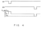
- Fig. 4 shows how the charge pump 12 functions.
- the switch 31 When the signal UP is low (logic 0), the switch 31 connects the node of output signal V out to V DD , and when the signal DN is low, the switch 32 connects the node to V SS .
- both signals UP and DN are high (logic 1), the node is isolated from V DD and V SS and voltage V op on a capacitor of loop filter (LPF) 13 appears as V out .
- LPF loop filter
- the loop filter 13 is a low-pass filter and is used to control the PLL dynamics and therefore the performance of the PLL.
- Voltage-controlled oscillator (VCO) 14 is a circuit that produces an AC (alternating current) output whose frequency F VCO is proportional to the input control voltage.
- 1/N divider 17 is a device that produces output signal D out whose frequency is an integer (denoted by N) division of that of an input signal (output signal X of the PLL). When the frequency of the signal X is F VCO , the frequency of the signal D out becomes F VCO /N.
- the signal D out is input as the signal FB to the phase comparator 11.
- 2-to-1 multiplexer (MUX) 15 makes it possible to by-pass the PLL with a clock signal at input A.
- S is the control input for the multiplexer 15.
- the PLL can be by-passed by setting input S to 0 and clocking through input A.
- a zero-pulse (pulse width given in specification) on S resets the PLL to a hold state.
- PLL testing may be achieved by exercising the PLL under test (PUT) as follows.
- the PLL like other high-frequency analog and mixed signal circuits, is difficult to test. Although most specification-based test schemes for the PLL perform the "start" sequence checks and normal mode operation verification, dynamic change of frequency and "stop” sequence checks are not facilitated for.
- Dalmia et al. have presented an operating current-monitoring method of PLL testing (M. Dalmia, A. Ivanov and S. Tabatabaei, "Power Supply Current Monitoring Techniques for Testing PLLs," Proc. Sixth IEEE Asian Test Symposium , pp. 366-371, November 1997).
- the approach used in this method is not ad-hoc, however, currently it is difficult to implement a test scheme based on operating current measurement.
- Kim et al. have presented a defect-oriented method that realizes testing by taking the PLL operation through two dynamic transitions (S. Kim, M. Soma and D. Risbud, "An Effective Defect-Oriented BIST Architecture for High-Speed Phase-LockedLoops, "Proc . 18th IEEE VLSI Test Symposium , April 2000). The method then measures the three stable frequencies for comparisons with the expected frequencies. However, their method does not perform the "start" sequence check and it requires the addition of a significant amount of extra hardware.
- the testing device comprises a reset circuit, an input circuit, an output circuit and a connection control circuit.
- the reset circuit resets the phase-locked loop by disconnecting the charge pump from the loop filter and providing an alternative discharge path for the loop filter.
- the input circuit receives a feedback signal from an output of the phase-locked loop and a control signal, produces a combination signal from the received signals and inputs the combination signal to the phase-locked loop.
- the combination signal together with a reference signal, causes the phase-locked loop to perform one of charging up the loop filter, discharging the loop filter and a normal operation.
- the output circuit outputs a signal with a frequency corresponding to an output of the voltage-controlled oscillator in cases that the phase-locked loop charges up the loop filter, that the phase-locked loop discharges the loop filter and that the phase-locked loop performs the normal operation.
- the connection control circuit controls connection between a digital circuit and an analog circuit of the phase-locked loop.
- FIG. 5 shows the principle of a testing device according to the present invention.
- the testing device comprises reset circuit 41, input circuit 42, output circuit 43 and connection control circuit 44.
- the reset circuit 41 resets PLL 45 by disconnecting the charge pump from the LPF and providing an alternative discharge path for the LPF.
- the input circuit 42 receives a feedback signal from an output of the PLL 45 and a control signal, produces a combination signal from the received signals and inputs the combination signal to the PLL 45.
- the combination signal together with a reference signal, causes the PLL 45 to perform one of charging up the LPF, discharging the LPF and a normal operation.
- the output circuit 43 outputs a signal with a frequency corresponding to an output of the VCO in cases that the PLL 45 is reset, when the PLL 45 charges up the LPF, that the PLL 45 discharges the LPF and that the PLL 45 performs the normal operation.
- the connection control circuit 44 controls connection between a digital circuit and an analog circuit of the PLL 45.
- the reset circuit 41 discharges the LPF for a period determined by the width of the reset pulse (a duration equal to the width).
- the feedback signal and the control signal are input to the PLL 45 and the PLL 45 can be exercised by transitions through various stable states, which include a charged-up state, a partially discharged state, a fully discharged state and a state of the normal operation. Since the frequency of the output signal from the output circuit 43 corresponds to that of the output signal of the VCO, pass/fail decision can be made by measuring the frequency at each of the states.
- the connection control circuit 44 isolates the digital circuit from the analog circuit or connects the digital circuit and the analog circuit according to need. Thus, the digital circuit can be tested separately from the analog circuit.
- the PLL 45 can be exercised well enough without making the output of the phase comparator directly controllable and a modified PLL testing is realized.
- the reset circuit 41 shown in Fig. 5 corresponds to a signal S and reset interfaces to the charge pump 12 and VCO 14 shown in Fig. 7, for example.
- the input circuit 42 shown in Fig. 5 corresponds to AND gate 51 and switches N1 and P1 shown in Fig. 7, and the output circuit 43 shown in Fig. 5 corresponds to MUX 15 and 1/N divider 17 shown in Fig. 7, for example .
- the connection control circuit 44 shown in Fig. 5 corresponds to the transistor switches P2, P3 and N2 shown in Fig. 7, for example.
- the reference signal shown in Fig. 5 corresponds to signal CK shown in Fig. 7, the combination signal shown in Fig. 5 corresponds to a signal input to lower inputs of phase comparator 11 and lock detector 16 shown in Fig. 7, and the output signal from the output circuit 43 shown in Fig. 5 corresponds to a signal at X or D out shown in Fig. 7, for example.
- the testing method of the present invention is a systematic method which has all the advantages of the methods of Dalmia et al. and Kim et al. mentioned earlier. It gives a clear description of test generation and performs the "start" sequence check, as well.
- the method of the invention has the following features.
- Fig. 6 shows the layout of the power supply for the PLL shown in Fig. 1.
- the separation of the power supply of the digital units (digital circuit) from the power supply of the analog units (analog circuit) is evident. This makes feasible the idea of isolating the digital units from the analog units during test.
- a two-phase approach is adopted for the testing of the PLL. In the first phase (Phase 1), only the digital components are tested. In this phase, the digital components (phase comparator 11, charge pump 12, MUX 15 and lock detector 16) of PUT are isolated from the analog components (LPF 13 and VCO 14), and then IDDQ and voltage tests are simultaneously conducted on them.
- the LPF 13 controls the performance of the PLL (and the effect of the LPF 13 is controllable) , varying the amount of charge stored on the capacitor of the LPF 13 (i.e. charging and discharging the capacitor) and allowing enough time to take measurements, provides a means of exercising the PLL while observing its response .
- the digital units are connected to the analog units and PUT is exercised by causing it to undergo a series of frequency transitions.
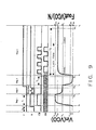
- V max and V min are the maximum and minimum voltages input to the VCO 14, respectively (see Fig. 9).
- the PLL is exercised by transition through four operating points corresponding to F max , F o , F min and the normal operating frequency, F op .
- F max , F o , F min and F op represent a maximum reference frequency, a center frequency, a minimum reference frequency and an expected normal operating frequency, respectively.
- a frequency measurement is taken after time intervals determined through transient analysis of the circuit. The measured values are compared against the good machine values to determine whether or not the PUT is fault-free within pre-computed tolerance limits. Determination of the good machine values and the tolerances on them is achieved through the analysis of reference values used in specification-based testing and through simulation.
- Fig. 7 shows the configuration of a testing device .
- the reset interfaces are actually included in the charge pump 12 and VCO 14.
- the LPF 13 is normally discharged through the lower transistor of the charge pump. However, during reset an alternative discharge path is provided in the reset interface to the charge pump 12 (partial discharge) .
- CR resistor-capacitor
- phase comparator 11 To facilitate the manipulation of the feedback input of the phase comparator 11, controllability has been introduced at the input of the phase comparator 11 (and hence of the lock detector 16).
- Two transistor switches N1 and P1 and AND gate 51 provide the controllability.
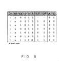
- the signals DT and t provide the controls.
- the AND gate 51 receives the signal t and feedback signal FB from the output of the PLL and produces a logical product of them.
- three transistor switches P2, P3 and N2 have been inserted to provide a means for partitioning the PLL into digital and analog sub-circuits in Phase 1.
- Digital sub-circuit isolation is controlled by the digital test signal DT.
- the 1/N divider 17 has been separately tested and found to be free of faults that might invalidate this testing.
- the circuit gets stable before the outputs are observed (or IDDQ observed).
- IDDQ testing cannot be carried out if even one gate is undergoing a transition during the time of observation.
- the signal DT must be set to logic 1.
- DT is set to logic 1.
- Phase 2 There are four steps in Phase 2 corresponding to the stages of the diagram shown in Fig. 9.
- the entire PUT is exercised together and frequency measurements are taken.
- the signal DT is set to logic 0 and the signal S is set to logic 0 long enough to ensure that the capacitor of the LPF 13 is at ground potential.
- V in (VCO) represents the input voltage v of the VCO 14 and F out (VCO)/N represents the output frequency at D out .
- D out is the target signal for frequency measurement.
- the testing procedure in each of the steps 1 through 4 is as follows.
- the good machine values of (and tolerances on) the reference frequencies F max , F o , F min and F op are set through simulations and from design specifications. If all measured quantities are within the tolerance range of their good machine values, PUT has 'passed' the test. Otherwise PUT has 'failed'.
- the frequencies may be also measured at X instead of D out if an appropriate measurement is applicable there.
- modified PLL testing which includes verification of dynamic change of frequency and/or a "start" sequence check, is realized with simple hardware.
Landscapes
- Engineering & Computer Science (AREA)
- General Engineering & Computer Science (AREA)
- Physics & Mathematics (AREA)
- General Physics & Mathematics (AREA)
- Stabilization Of Oscillater, Synchronisation, Frequency Synthesizers (AREA)
- Tests Of Electronic Circuits (AREA)
Abstract
Description
Steven L. Maddy, "Phase-Locked Loop," Chapter 70 of The Electrical Engineering Handbook, editor-in-chief: Richard C. Dorf, IEEE Press, CRC Press, pp. 1567-1575, 1993.
- Checking the "start" sequence: This is the verification that the PLL could be brought up to frequency within a specified time from the time the system is started. This includes the verification of phase locking.
- Normal mode operation: After phase lock, checks must be done to ascertain that the output signal of the PLL is at the desired frequency.
- Changing frequency dynamically: This is the verification of the fact that the PLL could operate in various modes, such as system test mode, normal operation mode, etc. This may involve the reprogramming of the PLL in order to effect frequency change dynamically.
- Checking the "stop" sequence: This is the verification that all chips being driven would stop at the stop of the PLL. This, together with the "start" sequence check, verifies that the driven chips would cease and resume operation in tandem.
- Step 1 (stage between time t-1 and t1) : Set t=CK=0. After time T0, set S to 1 and then change the value of CK to 1. Wait for T1 time units after the transition at CK and then, measure frequency F1 at Dout at time M1 (for the fault-free PLL F1=Fmax). T1 is the time it takes for the LPF capacitor to charge from ground voltage (0) up to Vmax.
- Step 2 (stage between time t1 and t2) : Set CK back to
0 and reset PUT to discharge the LPF capacitor until
the input voltage of the
VCO 14 is Vo=(Vmax+Vmin)/2. The time for achieving this partial discharge must be precomputed. Immediately after the reset, measure F2 at Dout at time M2 (for the fault-free PLL F2=Fo). After measurement, set t to 1. - Step 3 (stage between time t2 and t3): With CK still
at
logic 0, the first positive transition from FB causes the beginning of the complete discharge of The LPF capacitor. After time T3 from the last transition at t, measure F3 (expected to be equal to Fmin) at Dout at time M3. T3=2/Fo+τ; where τ is the time for complete discharge of the LPF capacitor. - Step 4 (stage between time t3 and t4) : Input operating
clock signal at CK while maintaining t at
logic 1 to allow the feedback clock signal to pass from FB. After time period T4 (T4 ≥ lock time + 1/ Fop), observe the value of L to ascertain a locked situation. Then, measure F4 (expected to be equal to Fop) at Dout at time M4. This step corresponds to a "start" sequence check (ascertaining locked condition by observing the output of thelock detector 16 after a specified time) and a normal mode operation verification (verifying the normal mode output frequency).
Claims (7)
- A testing device for a phase-locked loop (45) including a phase comparator (11), a charge pump (12), a loop filter (13) and a voltage-controlled oscillator (14), comprising:a reset circuit (41, S) for resetting the phase-locked loop by disconnecting the charge pump from the loop filter and providing an alternative discharge path for the loop filter;an input circuit (42, 51, N1, P1) for receiving a feedback signal (FB) from an output of the phase-locked loop and a control signal (t) , producing a combination signal from the received signals and inputting the combination signal to the phase-locked loop, the combination signal, together with a reference signal (CK), causing the phase-locked loop to perform one of charging up the loop filter, discharging the loop filter and a normal operation;an output circuit (15, 17, 43) for outputting a signal with a frequency corresponding to an output of the voltage-controlled oscillator in cases that the phase-locked loop charges up the loop filter, that the phase-locked loop discharges the loop filter and that the phase-locked loop performs the normal operation; anda connection control circuit (44, P2, P3,N2) for controlling connection between a digital circuit (11, 12, 15 and 16) and an analog circuit (13 and 14) of the phase-locked loop.
- The testing device according to claim 1, wherein:the digital circuit includes the phase comparator and the charge pump, and the analog circuit includes the loop filter and the voltage-controlled oscillator;said connection control circuit isolates the digital circuit from the analog circuit when the digital circuit is tested; andwhen the digital circuit is not isolated from the analog circuit, the combination signal, together with the reference signal, causes the phase-locked loop to perform one of charging up the loop filter, discharging the loop filter and the normal operation.
- The testing device according to claim 1 or 2, wherein:said input circuit inputs the combination signal to the phase comparator; andthe phase comparator produces input signals for the charge pump according to the combination signal.
- A testing method for a phase-locked loop (45) including a digital circuit (11, 12, 15 and 16) and an analog circuit (13 and 14), comprising:isolating the digital circuit from the analog circuit, the analog circuit including a loop filter (13) and a voltage-controlled oscillator (14);testing the digital circuit;connecting the digital circuit and the analog circuit;charging up the loop filter;measuring a frequency (F1) of a target signal corresponding to an output of the voltage-controlled oscillator and comparing the measured frequency with a maximum reference frequency (Fmax);resetting the phase-locked loop; andmeasuring the frequency (F2) of the target signal and comparing the measured frequency with a center frequency (Fo).
- A testing method for a phase-locked loop (45) including a digital circuit (11, 12, 15 and 16) and an analog circuit (13 and 14), comprising:isolating the digital circuit from the analog circuit, the analog circuit including a loop filter (13) and a voltage-controlled oscillator (14);testing the digital circuit;connecting the digital circuit and the analog circuit;resetting the phase-locked loop;measuring a frequency (F2) of a target signal corresponding to an output of the voltage-controlled oscillator and comparing the measured frequency with a center frequency (Fo);discharging the loop filter; andmeasuring the frequency (F3) of the target signal and comparing the measured frequency with a minimum reference frequency (Fmin).
- A testing method for a phase-locked loop (45) including a digital circuit (11, 12, 15 and 16) and an analog circuit (13 and 14), comprising:isolating the digital circuit from the analog circuit, the analog circuit including a loop filter (13) and a voltage-controlled oscillator (14);testing the digital circuit;connecting the digital circuit and the analog circuit;charging up the loop filter;measuring a frequency (F1) of a target signal corresponding to an output of the voltage-controlled oscillator and comparing the measured frequency with a maximum reference frequency (Fmax) ;resetting the phase-locked loop;measuring the frequency (F2) of the target signal and comparing the measured frequency with a center frequency (Fo) ;discharging the loop filter;measuring the frequency (F3) of the target signal and comparing the measured frequency with a minimum reference frequency (Fmin) ;causing the phase-locked loop to perform a normal operation; andmeasuring the frequency (F4) of the target signal and comparing the measured frequency with an expected normal operating frequency (Fop).
- A testing device for a phase-locked loop (45) including aphase comparator, a charge pump, a loop filter and a voltage-controlled oscillator, comprising:reset means (41 and S) for resetting the phase-locked loop by disconnecting the charge pump from the loop filter and providing an alternative discharge path for the loop filter;input means (42, 51, N1 and P1) for receiving a feedback signal (FB) from an output of the phase-locked loop and a control signal (t) , producing a combination signal from the received signals and inputting the combination signal to the phase-locked loop, the combination signal, together with a reference signal (CK), causing the phase-locked loop to perform one of charging up the loop filter, discharging the loop filter and a normal operation;output means (15, 17 and 43) for outputting a signal with a frequency corresponding to an output of the voltage-controlled oscillator in cases that the phase-locked loop charges up the loop filter, that the phase-locked loop discharges the loop filter and that the phase-locked loop performs the normal operation; andconnection control means (44, P2, P3 and N2) for controlling connection between a digital circuit (11, 12, 15 and 16) and an analog circuit (13 and 14) of the phase-locked loop.
Applications Claiming Priority (2)
| Application Number | Priority Date | Filing Date | Title |
|---|---|---|---|
| JP2001253300A JP3790689B2 (en) | 2001-08-23 | 2001-08-23 | Phase locked loop test apparatus and method |
| JP2001253300 | 2001-08-23 |
Publications (3)
| Publication Number | Publication Date |
|---|---|
| EP1286169A2 true EP1286169A2 (en) | 2003-02-26 |
| EP1286169A3 EP1286169A3 (en) | 2004-01-07 |
| EP1286169B1 EP1286169B1 (en) | 2005-10-19 |
Family
ID=19081652
Family Applications (1)
| Application Number | Title | Priority Date | Filing Date |
|---|---|---|---|
| EP02250454A Expired - Lifetime EP1286169B1 (en) | 2001-08-23 | 2002-01-23 | Device and method for testing phase-locked loops |
Country Status (4)
| Country | Link |
|---|---|
| US (1) | US6642701B2 (en) |
| EP (1) | EP1286169B1 (en) |
| JP (1) | JP3790689B2 (en) |
| DE (1) | DE60206714T2 (en) |
Cited By (2)
| Publication number | Priority date | Publication date | Assignee | Title |
|---|---|---|---|---|
| WO2005078464A1 (en) * | 2004-02-13 | 2005-08-25 | Koninklijke Philips Electronics N.V. | Method and device for testing a phase locked loop |
| CN108471309A (en) * | 2018-02-12 | 2018-08-31 | 中国科学院上海微系统与信息技术研究所 | A kind of lock detecting circuit for phaselocked loop |
Families Citing this family (12)
| Publication number | Priority date | Publication date | Assignee | Title |
|---|---|---|---|---|
| FR2832564B1 (en) * | 2001-11-19 | 2004-01-30 | Stepmind | PHASE AND FREQUENCY COMPARISON METHOD AND DEVICE |
| GB2393794B (en) * | 2002-10-01 | 2004-11-24 | Motorola Inc | Module, system and method for testing a phase locked loop |
| JP2005150152A (en) * | 2003-11-11 | 2005-06-09 | Seiko Epson Corp | Semiconductor device and PLL circuit |
| US6995554B2 (en) * | 2004-06-16 | 2006-02-07 | Agilent Technologies, Inc. | Delay-locked loop and a method of testing a delay-locked loop |
| US7019572B2 (en) | 2004-07-26 | 2006-03-28 | Kabushiki Kaisha Toshiba | Systems and methods for initializing PLLs and measuring VCO characteristics |
| US7205853B2 (en) | 2005-03-28 | 2007-04-17 | Kabushiki Kaisha Toshiba | Method to configure phase-locked loop dividing ratio |
| US7265634B2 (en) | 2005-06-17 | 2007-09-04 | Kabushiki Kaisha Toshiba | System and method for phase-locked loop initialization |
| US20100244878A1 (en) * | 2006-12-26 | 2010-09-30 | Yuji Yamada | Pll burn-in circuit and semiconductor integrated circuit |
| JP2008217947A (en) * | 2007-03-07 | 2008-09-18 | Elpida Memory Inc | Semiconductor memory |
| US9461546B2 (en) * | 2013-02-08 | 2016-10-04 | Advanced Charging Technologies, LLC | Power device and method for delivering power to electronic devices |
| CN109245761B (en) * | 2018-09-21 | 2021-07-02 | 电子科技大学 | A method of suspending and resuming a phase-locked loop |
| US12267082B2 (en) * | 2023-08-31 | 2025-04-01 | Nxp Usa, Inc. | Frequency-regulated oscillator circuit |
Family Cites Families (2)
| Publication number | Priority date | Publication date | Assignee | Title |
|---|---|---|---|---|
| US5257294A (en) * | 1990-11-13 | 1993-10-26 | National Semiconductor Corporation | Phase-locked loop circuit and method |
| US5359297A (en) * | 1993-10-28 | 1994-10-25 | Motorola, Inc. | VCO power-up circuit for PLL and method thereof |
-
2001
- 2001-08-23 JP JP2001253300A patent/JP3790689B2/en not_active Expired - Fee Related
-
2002
- 2002-01-18 US US10/050,863 patent/US6642701B2/en not_active Expired - Fee Related
- 2002-01-23 EP EP02250454A patent/EP1286169B1/en not_active Expired - Lifetime
- 2002-01-23 DE DE60206714T patent/DE60206714T2/en not_active Expired - Fee Related
Cited By (2)
| Publication number | Priority date | Publication date | Assignee | Title |
|---|---|---|---|---|
| WO2005078464A1 (en) * | 2004-02-13 | 2005-08-25 | Koninklijke Philips Electronics N.V. | Method and device for testing a phase locked loop |
| CN108471309A (en) * | 2018-02-12 | 2018-08-31 | 中国科学院上海微系统与信息技术研究所 | A kind of lock detecting circuit for phaselocked loop |
Also Published As
| Publication number | Publication date |
|---|---|
| DE60206714T2 (en) | 2006-05-18 |
| JP3790689B2 (en) | 2006-06-28 |
| EP1286169B1 (en) | 2005-10-19 |
| EP1286169A3 (en) | 2004-01-07 |
| US6642701B2 (en) | 2003-11-04 |
| JP2003069423A (en) | 2003-03-07 |
| DE60206714D1 (en) | 2006-03-02 |
| US20030038619A1 (en) | 2003-02-27 |
Similar Documents
| Publication | Publication Date | Title |
|---|---|---|
| EP1286169B1 (en) | Device and method for testing phase-locked loops | |
| US7737739B1 (en) | Phase step clock generator | |
| Sunter et al. | BIST for phase-locked loops in digital applications | |
| US5745011A (en) | Data recovery phase locked loop | |
| US6859028B2 (en) | Design-for-test modes for a phase locked loop | |
| JPH1138100A (en) | Semiconductor test device | |
| US8473792B2 (en) | Logic BIST for system testing using stored patterns | |
| Azaïs et al. | An all-digital DFT scheme for testing catastrophic faults in PLLs | |
| EP1293791B1 (en) | Semiconductor integrated circuit device and device for testing same | |
| US6671848B1 (en) | Test circuit for exposing higher order speed paths | |
| TWI381469B (en) | Semiconductor integrated circuit and method of testing same | |
| Georgoulopoulos et al. | UVM-based verification of a digital PLL using SystemVerilog | |
| Goteti et al. | DFT for embedded charge-pump PLL systems incorporating IEEE 1149.1 | |
| Kommey et al. | Design of a fully integrated VHF CP‐PLL frequency synthesizer with an all‐digital defect‐oriented built‐in self‐test | |
| Tiwari et al. | An innovative approach of computational fault detection using design for testability of CP-PLL | |
| US8154328B1 (en) | Techniques for measuring phases of periodic signals | |
| Han et al. | An efficient all-digital built-in self-test for chargepump PLL | |
| Kinger et al. | Experiences with parametric BIST for production testing PLLs with picosecond precision | |
| US7607061B2 (en) | Shrink test mode to identify Nth order speed paths | |
| Xia et al. | A methodology of fault detection using design for testability of cp-pll | |
| WO1998016005A1 (en) | Phase detector with explicit asynchronous reset | |
| Yu et al. | KGD testing technology in More than Moore Era | |
| KR100520441B1 (en) | Performance Test Device of DLL Using PLL and The Method | |
| Wang et al. | A novel BIST approach for testing DLLs of SoC | |
| Han et al. | An effective built-in self-test for chargepump PLL |
Legal Events
| Date | Code | Title | Description |
|---|---|---|---|
| PUAI | Public reference made under article 153(3) epc to a published international application that has entered the european phase |
Free format text: ORIGINAL CODE: 0009012 |
|
| AK | Designated contracting states |
Kind code of ref document: A2 Designated state(s): AT BE CH CY DE DK ES FI FR GB GR IE IT LI LU MC NL PT SE TR |
|
| AX | Request for extension of the european patent |
Extension state: AL LT LV MK RO SI |
|
| PUAL | Search report despatched |
Free format text: ORIGINAL CODE: 0009013 |
|
| AK | Designated contracting states |
Kind code of ref document: A3 Designated state(s): AT BE CH CY DE DK ES FI FR GB GR IE IT LI LU MC NL PT SE TR |
|
| AX | Request for extension of the european patent |
Extension state: AL LT LV MK RO SI |
|
| RIC1 | Information provided on ipc code assigned before grant |
Ipc: 7G 01R 31/30 B Ipc: 7G 01R 31/3167 A |
|
| 17P | Request for examination filed |
Effective date: 20040630 |
|
| 17Q | First examination report despatched |
Effective date: 20040802 |
|
| AKX | Designation fees paid |
Designated state(s): DE FR GB |
|
| GRAP | Despatch of communication of intention to grant a patent |
Free format text: ORIGINAL CODE: EPIDOSNIGR1 |
|
| GRAS | Grant fee paid |
Free format text: ORIGINAL CODE: EPIDOSNIGR3 |
|
| GRAA | (expected) grant |
Free format text: ORIGINAL CODE: 0009210 |
|
| AK | Designated contracting states |
Kind code of ref document: B1 Designated state(s): DE FR GB |
|
| REG | Reference to a national code |
Ref country code: GB Ref legal event code: FG4D |
|
| REF | Corresponds to: |
Ref document number: 60206714 Country of ref document: DE Date of ref document: 20060302 Kind code of ref document: P |
|
| ET | Fr: translation filed | ||
| PLBE | No opposition filed within time limit |
Free format text: ORIGINAL CODE: 0009261 |
|
| STAA | Information on the status of an ep patent application or granted ep patent |
Free format text: STATUS: NO OPPOSITION FILED WITHIN TIME LIMIT |
|
| 26N | No opposition filed |
Effective date: 20060720 |
|
| PGFP | Annual fee paid to national office [announced via postgrant information from national office to epo] |
Ref country code: DE Payment date: 20090115 Year of fee payment: 8 |
|
| PGFP | Annual fee paid to national office [announced via postgrant information from national office to epo] |
Ref country code: GB Payment date: 20090121 Year of fee payment: 8 |
|
| PGFP | Annual fee paid to national office [announced via postgrant information from national office to epo] |
Ref country code: FR Payment date: 20090113 Year of fee payment: 8 |
|
| GBPC | Gb: european patent ceased through non-payment of renewal fee |
Effective date: 20100123 |
|
| REG | Reference to a national code |
Ref country code: FR Ref legal event code: ST Effective date: 20100930 |
|
| PG25 | Lapsed in a contracting state [announced via postgrant information from national office to epo] |
Ref country code: FR Free format text: LAPSE BECAUSE OF NON-PAYMENT OF DUE FEES Effective date: 20100201 |
|
| PG25 | Lapsed in a contracting state [announced via postgrant information from national office to epo] |
Ref country code: DE Free format text: LAPSE BECAUSE OF NON-PAYMENT OF DUE FEES Effective date: 20100803 |
|
| PG25 | Lapsed in a contracting state [announced via postgrant information from national office to epo] |
Ref country code: GB Free format text: LAPSE BECAUSE OF NON-PAYMENT OF DUE FEES Effective date: 20100123 |