EP1284505A2 - Semiconductor integrated circuit device - Google Patents
Semiconductor integrated circuit device Download PDFInfo
- Publication number
- EP1284505A2 EP1284505A2 EP02255628A EP02255628A EP1284505A2 EP 1284505 A2 EP1284505 A2 EP 1284505A2 EP 02255628 A EP02255628 A EP 02255628A EP 02255628 A EP02255628 A EP 02255628A EP 1284505 A2 EP1284505 A2 EP 1284505A2
- Authority
- EP
- European Patent Office
- Prior art keywords
- lines
- metal
- polysilicon
- line
- length
- Prior art date
- Legal status (The legal status is an assumption and is not a legal conclusion. Google has not performed a legal analysis and makes no representation as to the accuracy of the status listed.)
- Withdrawn
Links
Images

Classifications
-
- H—ELECTRICITY
- H10—SEMICONDUCTOR DEVICES; ELECTRIC SOLID-STATE DEVICES NOT OTHERWISE PROVIDED FOR
- H10W—GENERIC PACKAGES, INTERCONNECTIONS, CONNECTORS OR OTHER CONSTRUCTIONAL DETAILS OF DEVICES COVERED BY CLASS H10
- H10W20/00—Interconnections in chips, wafers or substrates
- H10W20/40—Interconnections external to wafers or substrates, e.g. back-end-of-line [BEOL] metallisations or vias connecting to gate electrodes
- H10W20/41—Interconnections external to wafers or substrates, e.g. back-end-of-line [BEOL] metallisations or vias connecting to gate electrodes characterised by their conductive parts
- H10W20/44—Conductive materials thereof
- H10W20/4451—Semiconductor materials, e.g. polysilicon
Definitions
- the present invention relates to a plurality of metal lines each of which partially straps a different one of a plurality of polysilicon lines in a semiconductor integrated circuit device.
- Semiconductor integrated circuit devices are well known in the art.
- memory devices including both volatile (such as DRAM or SRAM) as well as nonvolatile (such as FLASH)
- a plurality of polysilicon lines are used as row lines to access various memory cells. Because these row lines are made out of polysilicon, they tend to have higher resistivity than conductors made out of metal.
- metal lines are used to "strap" various polysilicon lines. By strapping it is meant to connect a metal line in parallel with the polysilicon row line to reduce the resistivity of the polysilicon row line.
- the width of the polysilicon lines will also decrease.
- the scale of integration for metal lines has not kept pace at the same rate as the scale of integration for other features such as the polysilicon lines.
- the width of the metal strapping lines has not been reduced at the same rate as the width of the polysilicon lines.
- a metal line having a width greater than a plurality of polysilicon lines may be segmented into a plurality of metal segments with each metal segment used to strap a different one of the polysilicon lines.
- the present invention deals with the optimal position for the strapping of such a partial strapped polysilicon line.
- a semiconductor integrated circuit device comprises a semiconductor substrate with a plurality of circuits therein.
- a plurality of substantially parallel, laterally adjacent spaced apart polysilicon lines are insulated from the substrate and interconnect the plurality of circuits.
- Each of the plurality of polysilicon lines has a first end and a second end and has substantially the same length between the first end and the second end with electrical signals traversing from the second end to the first end.
- a plurality of substantially collinear metal lines are spaced apart from the plurality of polysilicon lines. Each of the plurality of metal lines electrically connects to a different one of the plurality of polysilicon lines.
- the metal line at the second end has a length of 4 / 3x where L is the length between the first end and the second end and n is the number of metal lines.
- the semiconductor integrated circuit device 10 comprises a semiconductor substrate in which a plurality of circuits 12 are formed.
- a plurality of substantially parallel laterally adjacent spaced apart polysilicon lines 14(a-n) are formed above and insulated from the substrate. They interconnect the plurality of circuits 12.
- Each of the plurality of polysilicon lines 14(a-n) has a second end 20 and a first end 22 with substantially the same length between the first end 22 and the second end 20 with electrical signals traversing from the second end 20 to the first end 22.
- the integrated circuit device 10 is a memory device in which the plurality of circuits 12 are row decoders.
- the plurality of polysilicon lines 14(a-n) are word lines or row lines.
- the semiconductor integrated circuit device 10 can be a volatile memory device such as a DRAM or an SRAM or can be a non-volatile memory device such as a FLASH memory device or an EEPROM device.
- each of the polysilicon lines 14a and 14b has a first end 22 and a second end 20 and a length therebetween with each having a width of a dimension P, with P less than d. In fact, d overlaps the distance between the two polysilicon lines 14a and 14b as well as including their widths P.
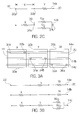
- the metal line 30 has two segments 30a and 30b having a length of x and y respectively. Each of the lengths x and y is used to strap or is connected to a different one of the polysilicon lines 14a or 14b.
- the metal segment 30a is used to strap polysilicon line 14a through via holes 32a and 32b.
- the metal segment 30b is used to strap polysilicon line 14b through the via holes 34a and 34b.
- Polysilicon line 14a extends from the first end 22 to the second end 20 through a line having resistivity as shown by the waviness of the line in Figure 2b.
- the metal segment 30a having a length of x straps the polysilicon line 14a. There is essentially no resistance between the location of the via hole 32a and 32b
- the polysilicon line 14b is shown as being “wavy” indicating that it has a resistivity between the first end 22 and the second end 20. However, between the via hole 34a and 34b the metal segment 30b having a length of y is used to strap the polysilicon line 14b.
- FIG. 2C there is shown a schematic circuit diagram of the strapping shown in Figure 2a.
- the polysilicon line 14a there is essentially zero resistivity between via hole 32a and 32b. Thereafter, between the via hole 32b and the second end 20, the resistivity is y which is the length of the polysilicon 14A which is not strapped. Thus, if a signal were to propagate from the second end 20 to the first end 22, it would encounter a resistivity path of length y followed by zero resistance.
- a similar analysis of the polysilicon line 14b shows that near the first end 22, of a distance x, the polysilicon line 14b has a resistivity of x.
- metal segment 30a is not the same length as metal segment 30b.
- the metal line 30 used to strap three polysilicon lines 14a, 14b and 14c comprises three segments 30a, 30b and 30c each having lengths x, y and w respectively.
- Metal segment 30a connects to polysilicon line 14a at via holes 32a and 32b and has a length x.
- Metal segment 30b connects to the polysilicon line 14b at via holes 34a and 34b and has the length y.
- Metal segment 30c connects to the polysilicon line 14c at via holes 36a and 36b and has a length w.
- the metal segments 30a, 30b and 30c are spaced apart from one another but are collinear.
- the invention as used and applied to three polysilicon lines 14a, 14b and 14c may be schematically shown as in Figure 3b.
- the signal propagating from the second end 20 to the first end 22 passes through a resistivity network comprising of resistance W and Y.
- the signal propagating from the second end 20 to the first end 22 passes through resistance of W and X.
- the signal line propagating from the second end 20 to the first end 22 passes through a network comprising of two resistors each with resistance W/2 connected in parallel, then in series with resistors X and Y. Since the signal propagation time for all three must be equal, one can solve the following equations and determine the optimal lengths for X, Y and W as follows:
- Equations (10), (11) and (12) must all be equal. Solving equation (10) and (11), one obtains:
- each of the above examples including the generalized example shows that in the case of partial strapping, the positioning of the metal segments and the lengths of the metal segments used in partial strapping is asymmetrical which is contrary to "intuitive" belief.
Landscapes
- Design And Manufacture Of Integrated Circuits (AREA)
Abstract
A method and apparatus for partially strapping a
plurality of polysilicon lines (14a,14b,14c), each having
a first end (22) and second end (20), uses a metal line
having a plurality of spaced apart metal segments
(30a,30b,30c) that are colinear with each metal segment
partially strapping a different one of the polysilicon
lines. The metal segments (30a,30b,30c) are arranged from
the first end (22) to the second end (20) with the signals
propagating from the second end (20) to the first end (22).
Each metal segment has a length x= L / n + 1/3 except the metal
segment at the second end (20) which has a length (4/3)x
where L is the length between the first end (22) and the
second end (20) and n is the number of metal segments.
Description
- The present invention relates to a plurality of metal lines each of which partially straps a different one of a plurality of polysilicon lines in a semiconductor integrated circuit device.
- Semiconductor integrated circuit devices are well known in the art. In particular, in the field of memory devices, including both volatile (such as DRAM or SRAM) as well as nonvolatile (such as FLASH), a plurality of polysilicon lines are used as row lines to access various memory cells. Because these row lines are made out of polysilicon, they tend to have higher resistivity than conductors made out of metal. Thus, metal lines are used to "strap" various polysilicon lines. By strapping it is meant to connect a metal line in parallel with the polysilicon row line to reduce the resistivity of the polysilicon row line.
- As the scale of integration increases, i.e., the smallest dimension of a feature in a semiconductor integrated circuit device decreases, the width of the polysilicon lines will also decrease. However, the scale of integration for metal lines has not kept pace at the same rate as the scale of integration for other features such as the polysilicon lines. In other words, the width of the metal strapping lines has not been reduced at the same rate as the width of the polysilicon lines.
- Thus, a metal line having a width greater than a plurality of polysilicon lines, may be segmented into a plurality of metal segments with each metal segment used to strap a different one of the polysilicon lines. The present invention deals with the optimal position for the strapping of such a partial strapped polysilicon line.
- In the present invention, a semiconductor integrated circuit device comprises a semiconductor substrate with a plurality of circuits therein. A plurality of substantially parallel, laterally adjacent spaced apart polysilicon lines are insulated from the substrate and interconnect the plurality of circuits. Each of the plurality of polysilicon lines has a first end and a second end and has substantially the same length between the first end and the second end with electrical signals traversing from the second end to the first end. A plurality of substantially collinear metal lines are spaced apart from the plurality of polysilicon lines. Each of the plurality of metal lines electrically connects to a different one of the plurality of polysilicon lines. The metal lines are arranged from the first end to the second end with each metal line having a length of X = L / n + 1/3. The metal line at the second end has a length of 4 / 3x where L is the length between the first end and the second end and n is the number of metal lines.
-
- Figure 1 is a top view of an integrated circuit device with a plurality of substantially parallel polysilicon lines to which the method and apparatus of the present invention can be applied.
- Figure 2A is a top view of one embodiment of the present invention in which a metal line partially straps two polysilicon lines.
- Figure 2B is a schematic view of the embodiment shown in Figure 2A.
- Figure 2C is an equivalent circuit of the invention shown in Figure 2A.
- Figure 3A is a top view of another embodiment of the present invention in which a metal line partially straps three polysilicon lines.
- Figure 3B is an equivalent circuit view of the invention shown in Figure 3A.
-
- Referring to Figure 1, there is shown a top level view of a semiconductor integrated
circuit device 10 to which the method and apparatus of the present invention can be applied. The semiconductorintegrated circuit device 10 comprises a semiconductor substrate in which a plurality ofcircuits 12 are formed. A plurality of substantially parallel laterally adjacent spaced apart polysilicon lines 14(a-n) are formed above and insulated from the substrate. They interconnect the plurality ofcircuits 12. Each of the plurality of polysilicon lines 14(a-n) has asecond end 20 and afirst end 22 with substantially the same length between thefirst end 22 and thesecond end 20 with electrical signals traversing from thesecond end 20 to thefirst end 22. - In the preferred embodiment, the
integrated circuit device 10 is a memory device in which the plurality ofcircuits 12 are row decoders. The plurality of polysilicon lines 14(a-n) are word lines or row lines. The semiconductor integratedcircuit device 10 can be a volatile memory device such as a DRAM or an SRAM or can be a non-volatile memory device such as a FLASH memory device or an EEPROM device. - Referring to Figures 2A-2C, there is shown one embodiment of the present invention in which a single metal line 30 is used to strap two adjacent spaced-apart
polysilicon lines polysilicon lines first end 22 and asecond end 20 and a length therebetween with each having a width of a dimension P, with P less than d. In fact, d overlaps the distance between the twopolysilicon lines - As previously stated, the metal line 30 has two
segments polysilicon lines metal segment 30a is used to strappolysilicon line 14a through viaholes metal segment 30b is used to strappolysilicon line 14b through thevia holes - Schematically this is shown in Figure 2b. Polysilicon
line 14a extends from thefirst end 22 to thesecond end 20 through a line having resistivity as shown by the waviness of the line in Figure 2b. However, between thevia holes metal segment 30a having a length of x straps thepolysilicon line 14a. There is essentially no resistance between the location of thevia hole - Similarly, the
polysilicon line 14b is shown as being "wavy" indicating that it has a resistivity between thefirst end 22 and thesecond end 20. However, between thevia hole metal segment 30b having a length of y is used to strap thepolysilicon line 14b. - Referring to Figure 2C there is shown a schematic circuit diagram of the strapping shown in Figure 2a. For the
polysilicon line 14a, there is essentially zero resistivity between viahole via hole 32b and thesecond end 20, the resistivity is y which is the length of the polysilicon 14A which is not strapped. Thus, if a signal were to propagate from thesecond end 20 to thefirst end 22, it would encounter a resistivity path of length y followed by zero resistance. A similar analysis of thepolysilicon line 14b shows that near thefirst end 22, of a distance x, thepolysilicon line 14b has a resistivity of x. However, near thesecond end 20, if the signal were generated at a point midway between the two viaholes node 34a from which then it encounters the resistivity of x. In short, in the segment between thevia hole - Because for both of these
polysilicon lines second end 20 and thefirst end 22 must be the same, one can set up the following equations. - 1) x + y = L L is the length of
polysilicon lines - 2) y + o = time of propagation of signal on
line 14a - 3) x + y / 4 = time of propagation of signal on
line 14b
Since - 4) y + o = X + y / 4
- 5) X = 3 / 4y
- 6) 3 / 4y + y = L
- 7) y = 4 / 7L
- 8) x = 3 / 7L
-
- In other words,
metal segment 30a is not the same length asmetal segment 30b. - Referring to Figure 3a, there is shown the method and apparatus of the present invention used to strap three
polysilicon lines polysilicon lines segments Metal segment 30a connects topolysilicon line 14a at viaholes Metal segment 30b connects to thepolysilicon line 14b at viaholes Metal segment 30c connects to thepolysilicon line 14c at viaholes 36a and 36b and has a length w. Themetal segments polysilicon lines polysilicon line 14a, the signal propagating from thesecond end 20 to thefirst end 22 passes through a resistivity network comprising of resistance W and Y. For thepolysilicon line 14b, the signal propagating from thesecond end 20 to thefirst end 22 passes through resistance of W and X. For thepolysilicon line 14c, the signal line propagating from thesecond end 20 to thefirst end 22 passes through a network comprising of two resistors each with resistance W/2 connected in parallel, then in series with resistors X and Y. Since the signal propagation time for all three must be equal, one can solve the following equations and determine the optimal lengths for X, Y and W as follows: - 9) x + y + w = L L is the length of
polysilicon lines - 10) w + y + o = time of propagation of signal on
line 14a. - 11) w + o + x = time of propagation of signal on
line 14b - 12) w / 4 + y + x = time of propagation of signal on
line 14c. -
- Equations (10), (11) and (12) must all be equal. Solving equation (10) and (11), one obtains:
- 13) x=y
-
- From this substituting into equations (10) and (12) one finds:
- 14) w = 4 / 3y
-
- Substituting (13) and (14) into equation (9) yields:
- Finally, one can "generalize" the case of partial strapping involving a single collinear metal line having a plurality of spaced apart metal segments partially strapping a plurality of polysilicon lines with each metal segment strapping a different polysilicon line, as follows:
- 15) a + b + ... + n-1 + x = L L is the length of
polysilicon lines - 16) o + b + ... + x = time of propagation of signal on
line 14a. - 17) a + 0 + c + ... + x = time of propagation of signal on
line 14b. - 18) a + b + o + d + ... + x = time of propagation of signal on
line 14c. -
- Four equations 16-18 ... it can be shown that
- (19) a = b = c = d = ... = n-1
-
- Finally, it can be shown that
- 20) a = b = c = d = ... n-1 = L / n + 1/3, n is the number of lines and
- 21) x = 4 / 3a, x is the segment closest to the
second end 20. -
- As can be seen from the foregoing, each of the above examples, including the generalized example shows that in the case of partial strapping, the positioning of the metal segments and the lengths of the metal segments used in partial strapping is asymmetrical which is contrary to "intuitive" belief.
Claims (13)
- A semiconductor integrated circuit device comprising:a semiconductor substrate;a plurality of circuits in said semiconductor substrate;a plurality of substantially parallel, laterally adjacent spaced part polysilicon lines, insulated from said substrate and interconnecting said plurality of circuits; each of said plurality of polysilicon lines having a first end and a second end and having substantially the same length between said first end and said second end with electrical signals traversing from said second end to said first end;a plurality of substantially collinear metal lines, spaced apart from said plurality of polysilicon lines;each of said plurality of metal lines for electrically connecting to a different one of said plurality of polysilicon lines;said metal lines arranged from said first end to said second end, with each metal line having a length ofand with the metal line at said second end having a length of 4/3X where L is the length between said first end and said second end, and n is the number of metal lines.
- The device of claim 1 wherein said integrated circuit device is a memory device.
- The device of claim 2 wherein said plurality of polysilicon lines are row lines.
- The device of claim 1 wherein the number of plurality of metal lines is two (2) and the lengths of the metal lines are X 1 = 3 / 7L; X 2 = 4 / 7 L with X 2 being the metal line at said second end.
- The device of claim 1 wherein the number of plurality of metal lines is three (3) and the lengths of the metal lines are X1 = 3 / 10 L; X 2 = 3 / 10 L; X 3 = 4 / 10L with X 3 being the metal 10 10 10 line at said second end.
- The device of claim 3 wherein said device is a volatile memory device.
- The device of claim 6 wherein said device is a DRAM.
- The device of claim 6 wherein said device is a SRAM.
- The device of claim 3 wherein said device is a non-volatile memory device.
- The device of claim 9 wherein said device is a flash memory device.
- A method of strapping a plurality of parallel laterally adjacent, spaced apart, polysilicon lines, insulated from a semiconductor substrate, wherein each of said plurality of polysilicon lines has a first end and a second end with substantially the same length with signals traversing from said second end to said first end; said method comprising:connecting a plurality of substantially collinear metal lines to said plurality of polysilicon lines; each metal line electrically strapping a different one of said plurality of polysilicon lines; said metal lines arranged from said first end to said second end with each metal line having a length ofand with the metal line at said second end having a length of 4 /3X where L is the length between said first end and said second end, and n is the number of metal lines.
- The method of claim 11 wherein the number of plurality of metal lines is two (2) and the lengths of the metal lines are X 1= 3 / 7L and X 2= 4 / 7L with X 2 being the metal line at said second end.
- The method of claim 11 wherein the number of plurality of metal lines is three (3) and the lengths of the metal lines are X 1 = 3 / 10L; X 2 = 3 / 10 L and X 3= 4 / 10L with X 3 being the metal lines at said second end.
Applications Claiming Priority (2)
| Application Number | Priority Date | Filing Date | Title |
|---|---|---|---|
| US09/930,811 US6455942B1 (en) | 2001-08-15 | 2001-08-15 | Method and apparatus for strapping a plurality of polysilicon lines in a semiconductor integrated circuit device |
| US930811 | 2001-08-15 |
Publications (1)
| Publication Number | Publication Date |
|---|---|
| EP1284505A2 true EP1284505A2 (en) | 2003-02-19 |
Family
ID=25459807
Family Applications (1)
| Application Number | Title | Priority Date | Filing Date |
|---|---|---|---|
| EP02255628A Withdrawn EP1284505A2 (en) | 2001-08-15 | 2002-08-13 | Semiconductor integrated circuit device |
Country Status (2)
| Country | Link |
|---|---|
| US (1) | US6455942B1 (en) |
| EP (1) | EP1284505A2 (en) |
Families Citing this family (2)
| Publication number | Priority date | Publication date | Assignee | Title |
|---|---|---|---|---|
| US8081670B2 (en) * | 2006-02-14 | 2011-12-20 | Digital Signal Corporation | System and method for providing chirped electromagnetic radiation |
| US7592705B2 (en) * | 2006-11-14 | 2009-09-22 | Silicon Storage Technology, Inc. | Method and apparatus for strapping two polysilicon lines in a semiconductor integrated circuit device |
Family Cites Families (3)
| Publication number | Priority date | Publication date | Assignee | Title |
|---|---|---|---|---|
| JPH08330536A (en) * | 1995-05-31 | 1996-12-13 | Hitachi Ltd | Semiconductor memory device and computer system using the same |
| US6043562A (en) * | 1996-01-26 | 2000-03-28 | Micron Technology, Inc. | Digit line architecture for dynamic memory |
| US5933725A (en) * | 1998-05-27 | 1999-08-03 | Vanguard International Semiconductor Corporation | Word line resistance reduction method and design for high density memory with relaxed metal pitch |
-
2001
- 2001-08-15 US US09/930,811 patent/US6455942B1/en not_active Expired - Lifetime
-
2002
- 2002-08-13 EP EP02255628A patent/EP1284505A2/en not_active Withdrawn
Also Published As
| Publication number | Publication date |
|---|---|
| US6455942B1 (en) | 2002-09-24 |
Similar Documents
| Publication | Publication Date | Title |
|---|---|---|
| TWI696275B (en) | Memory device and method for manufacturing the same | |
| KR102890571B1 (en) | Self-aligned vertical integration of three-terminal memory devices | |
| TWI712962B (en) | Neural network system | |
| KR102393976B1 (en) | Semiconductor memory devices | |
| DE102019122665A1 (en) | Semiconductor device | |
| US20020127775A1 (en) | Redistributed bond pads in stacked integrated circuit die package | |
| US9425209B1 (en) | Multilayer 3-D structure with mirror image landing regions | |
| CN102522624A (en) | Antenna coil and antenna device | |
| US11830805B2 (en) | Vertical memory device | |
| EP1313138A2 (en) | Protective layer in memory device and method therefore | |
| JP2892732B2 (en) | Integrated circuit device | |
| US20030062966A1 (en) | Method, memory system and memory module board for avoiding local incoordination of impedance around memory chips on the memory system | |
| KR930001737B1 (en) | Wordline array method of semiconductor memory device | |
| US11901363B2 (en) | Resistance measuring structures of stacked devices | |
| US6455942B1 (en) | Method and apparatus for strapping a plurality of polysilicon lines in a semiconductor integrated circuit device | |
| US6459119B1 (en) | Contact array structure for buried type transistor | |
| US11715513B2 (en) | Apparatuses and methods for sense line architectures for semiconductor memories | |
| EP0368646A1 (en) | Semiconductor device | |
| KR100278656B1 (en) | Semiconductor memory device having twisted bitlines | |
| CN111293117A (en) | Integrated assembly including redundant routing lines, and integrated circuit level having openings extending therethrough | |
| EP0100676A2 (en) | Resistors in semiconductor devices | |
| JP3173456B2 (en) | Semiconductor storage device | |
| US6037638A (en) | Semiconductor memory device | |
| US6550039B2 (en) | Circuit design method for designing conductive members with a multilayered structure to have antenna sized of proper values | |
| US7829459B2 (en) | Method and apparatus for strapping two polysilicon lines in a semiconductor integrated circuit device |
Legal Events
| Date | Code | Title | Description |
|---|---|---|---|
| PUAI | Public reference made under article 153(3) epc to a published international application that has entered the european phase |
Free format text: ORIGINAL CODE: 0009012 |
|
| AK | Designated contracting states |
Designated state(s): AT BE BG CH CY CZ DE DK EE ES FI FR GB GR IE IT LI LU MC NL PT SE SK TR |
|
| AX | Request for extension of the european patent |
Extension state: AL LT LV MK RO SI |
|
| STAA | Information on the status of an ep patent application or granted ep patent |
Free format text: STATUS: THE APPLICATION IS DEEMED TO BE WITHDRAWN |
|
| 18D | Application deemed to be withdrawn |
Effective date: 20050301 |