EP1284487A2 - Transformer shielding - Google Patents
Transformer shielding Download PDFInfo
- Publication number
- EP1284487A2 EP1284487A2 EP02102123A EP02102123A EP1284487A2 EP 1284487 A2 EP1284487 A2 EP 1284487A2 EP 02102123 A EP02102123 A EP 02102123A EP 02102123 A EP02102123 A EP 02102123A EP 1284487 A2 EP1284487 A2 EP 1284487A2
- Authority
- EP
- European Patent Office
- Prior art keywords
- shielding device
- accordance
- core portion
- electrical
- conductive material
- Prior art date
- Legal status (The legal status is an assumption and is not a legal conclusion. Google has not performed a legal analysis and makes no representation as to the accuracy of the status listed.)
- Granted
Links
Images

Classifications
-
- H—ELECTRICITY
- H01—ELECTRIC ELEMENTS
- H01F—MAGNETS; INDUCTANCES; TRANSFORMERS; SELECTION OF MATERIALS FOR THEIR MAGNETIC PROPERTIES
- H01F27/00—Details of transformers or inductances, in general
- H01F27/28—Coils; Windings; Conductive connections
- H01F27/288—Shielding
- H01F27/2885—Shielding with shields or electrodes
-
- H—ELECTRICITY
- H01—ELECTRIC ELEMENTS
- H01F—MAGNETS; INDUCTANCES; TRANSFORMERS; SELECTION OF MATERIALS FOR THEIR MAGNETIC PROPERTIES
- H01F27/00—Details of transformers or inductances, in general
- H01F27/34—Special means for preventing or reducing unwanted electric or magnetic effects, e.g. no-load losses, reactive currents, harmonics, oscillations, leakage fields
- H01F27/36—Electric or magnetic shields or screens
-
- H—ELECTRICITY
- H01—ELECTRIC ELEMENTS
- H01F—MAGNETS; INDUCTANCES; TRANSFORMERS; SELECTION OF MATERIALS FOR THEIR MAGNETIC PROPERTIES
- H01F27/00—Details of transformers or inductances, in general
- H01F27/34—Special means for preventing or reducing unwanted electric or magnetic effects, e.g. no-load losses, reactive currents, harmonics, oscillations, leakage fields
- H01F27/36—Electric or magnetic shields or screens
- H01F27/363—Electric or magnetic shields or screens made of electrically conductive material
-
- H—ELECTRICITY
- H01—ELECTRIC ELEMENTS
- H01F—MAGNETS; INDUCTANCES; TRANSFORMERS; SELECTION OF MATERIALS FOR THEIR MAGNETIC PROPERTIES
- H01F27/00—Details of transformers or inductances, in general
- H01F27/28—Coils; Windings; Conductive connections
- H01F27/32—Insulating of coils, windings, or parts thereof
- H01F27/324—Insulation between coil and core, between different winding sections, around the coil; Other insulation structures
Definitions
- the invention relates to electrical transformers, and more particularly to shielding of transformers to reduce interference due to electromagnetic radiation.
- an electrical transformer for converting a first voltage to a second voltage includes a core which includes a first core portion and a second core portion.
- the electrical transformer device further includes a shielding device, for electrically shielding said first core portion from said second core portion.
- the transformer incorporating the invention is a component in switching circuitry, such as an amplifier or power supply.
- a power supply for an electronic device includes input terminals for inputting line electrical power, a rectifier, for rectifying said line electrical power to produce rectified electrical power, a switching circuit, for switching said rectified electrical power to produce switched rectified electrical power, a transformer, for modifying said voltage.
- the transformer includes a core comprising a first core portion and a second core portion and a first shielding device, for electrically shielding said first core portion from said second core portion.
- an electronic device in another aspect of the invention, includes an antenna, for receiving radio frequency signals, a tuner, for tuning said radio frequency signals, and a switching power supply, for providing electrical power to said tuner.
- the switching power supply includes a transformer that has a first core portion, a second core portion, primary windings, and secondary windings.
- the transformer further includes a shielding device, for electrically shielding said first core portion from said second core portion.
- an electrical transformer has a first core portion, a second core portions, first windings, and second windings.
- a shielding device is designed and constructed to shield said first core portion from said second core portion.
- Transformer assembly 10 includes a core 12 consisting of two sections 12a and 12b.
- Primary winding 14 is wound around first core portion 12a
- secondary winding 16 is wound around second core portion 12b.
- Electrostatic shield 22 electrically isolates primary winding 12 from secondary winding 16 and also electrically isolates core first core portion 12a from second core portion 12b. Electrostatic shield 22 will be discussed more fully below.
- Plastic bobbin 24 may be provided to hold core portions 12a and 12b in place, to facilitate the formation of the primary and secondary windings, to provide connecting pins 24 for electrical connections to other devices, and to provide a mechanical support for the core portions 12a and 12b.
- First core portion 12a and second core portion 12b are "E" shaped and reverse “E” shaped blocks of a substance, such as ferrite that has a high magnetic permeability.
- Other shapes for the core portions include “C” and reverse “C” shapes, half-rings, and many others.
- Electrostatic shield 22 is shaped and positioned such that it lies between the first core portion and the second core portion, and may be further positioned such that it lies between the primary winding and the secondary winding.
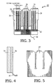
- Electrostatic shield 22 includes a substrate 26 of printed circuit board substrate material. On one surface (hereinafter the conductive surface) of the substrate 26 is a pattern 28 of an electrically conductive material such as copper, in a comb-type pattern consisting of parallel traces 29 of copper electrically connected at one end by a connecting trace 32.
- a drain wire 30 (or some other electrically conductive component) is electrically connected to the connecting trace 32 of the pattern of electrically conductive material and is connectable to a circuit portion which conducts capacitive displacement currents to their source.
- other patterns of conductive material can be used.
- a desirable characteristic of the patterns is that they avoid large area loops which would conduct significant eddy currents which could interfere with the magnetic field of the core 12.
- substrate 26 is 0.2 mm thick and 44.7mm wide.
- the electrostatic shield is positioned such that the conductive surface faces the primary winding 14 and first core portion 12a.
- the implementation of FIG. 3 may be constructed and arranged such that the conductive pattern 28 is in electrical contact with first core portion 12a so that any electrical currents that may occur in first core portion 12a are conducted away by drain wire 30.
- FIG. 4 there is shown a cross section taken along line 4 - 4 of FIG. 2 of a second implementation of the electrostatic shield 22.
- a thin layer of electrically insulating material 34 such as 0.2 mm thick polyester is covered with a thin conductive layer 36 (such as indium tin oxide).
- the thickness and the electrical characteristics of the conductive layer are selected such that the surface conductivity is about 20 ohms per square and so that there are only insignificant eddy currents in the conductive layer which have an insignificant effect on the magnetic field of the core 12.
- the dimensions and electrical characteristics of the conductive layer are further selected such that there is sufficient electrical conductivity to return capacitive displacement electrical currents to a drain wire 30 so that the capacitive displacement currents can be returned to their source.
- the shield of FIG. 5 is a sheet 37 of substantially uniformly conductive material, with a surface resistivity in the range of 10 ohms to 100 ohms per square.
- the physical and electrical dimensions of the sheet are selected such that there is sufficient conductivity to return capacitive displacement currents to drain wire 30, and so that the effect on the magnetic field of the core 12 is insignificant.
- a sheet of carbon impregnated polymer, 0.2 mm thick is suitable.
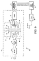
- An audio system 40 includes a switching power supply 42 which receives electrical power from a power plug 44 which is connectable to an outside source of electrical power (such as line AC power).
- Switching power supply 42 converts the line electrical power to electrical power for an audio signal amplification and transduction circuitry 46.
- the audio signal amplification and transduction circuitry 46 amplifies and transduces to sound waves audio signals from audio signal processor 48.
- Audio signal processor 48 processes audio signals from a number of sources, including AM/FM tuner 50.
- AM/FM tuner 52 receives and tunes radio signal received from antenna 52.
- Switching power supply 42 includes a first rectifier 54 and a switching circuit 56 coupled to transformer 10 according to the invention.
- Transformer 10 includes an electrostatic shield 22 positioned between the two core portions 12a and 12b, and between the primary winding 14 and secondary winding 16, with the conductive pattern (28 of FIG. 3 or 36 of FIG. 4) facing primary winding 14 and first core portion 12a.
- Drain wire 30 connects conductive pattern (28 of FIG. 3 or 36 of FIG. 4) of electrostatic shield 22 to switching circuit 56.
- Optional second electrostatic shield 22' is positioned between two core portions 12a and 12b and between primary winding 14 and secondary winding 16, with the conductive pattern or layer (28 of FIG. 3 or 36 of FIG. 4) of electrostatic shield 22' facing secondary winding 16 and second core portion 12b.
- Drain wire 30' of electrostatic shield 22' connects conductive pattern to a common lead 49 to secondary winding 16. Terminals of secondary winding 16 are coupled to second rectifier 58, which is coupled to audio signal amplification and transduction circuitry 16, which amplifies and transduces audio signals received from audio signal processor 48.
- the switching circuit 56 may modulate the voltage on the secondary windings 16 by a number of methods, including frequency modulation, pulse modulation, or pulse width modulation, and others.
- An alternative arrangement of the combination of electrostatic shield 22 and electrostatic shield 22' is a single electrically insulative substrate of sufficient thickness with a first conductive pattern or layer (28 of Fig. 3 or 36 Fig. 4) on a surface of the substrate facing first core portion 12a and primary winding 14 and a second conductive pattern or layer (28 of Fig. 3 or 36 Fig. 4) on a second surface of the substrate facing second core portion 12b and secondary winding 16.
- rectifier 54 rectifies AC line electrical power to DC electrical power.
- Switching circuit 56 converts the DC electrical power to electrical pulses, typically of a significantly higher frequency than the AC line electrical power.
- Transformer 10 transforms the electrical pulses to a different, typically lower, voltage.
- Second rectifier 58 converts the high frequency output of transformer 10 to DC of an appropriate voltage to power audio signal amplification and transduction circuitry 16.
- Audio signal amplification and transduction circuitry 16 amplifies and transduces audio signals received from audio signal processor 48.
- the voltage level at the output terminals of rectifier 58 is modulated by the switching circuit 56. Modulation may be done by a number of methods, including frequency modulation, pulse modulation, or pulse width modulation, and others.
- First electrostatic shield 22 and second electrostatic shield 22' shield conduct any capacitive displacement electrical currents back to the source of the electrical currents, thereby minimizing electromagnetic radiation from transformer assembly 10.
- An electronic device is advantageous because capacitive displacement charges between both windings and between core halves are significantly attenuated. There is therefore less need for EMI filtering of power line and output wires. Additionally, since a device incorporating the invention produces less electromagnetic interference, there is less need for EMI shielding of the device relative to nearby electronic devices components or devices.
- the shield can be manufactured inexpensively and integrated into the transformer easily. A transformer incorporating the shield has less need for more expensive EMI shielding devices that may be more difficult to assemble and may interfere with other functions, such as preventing overheating of the transformer.
- multiple shields may be employed to shield one core portion from two or more other core portions.
- a transformer shield according to the invention inhibits capacitive displacement currents flowing between core portions of a transformer without significantly affecting the magnetic properties of the core portions.
- a transformer incorporating the invention may have significantly less EMI radiation than conventional transformers.
Landscapes
- Engineering & Computer Science (AREA)
- Power Engineering (AREA)
- Shielding Devices Or Components To Electric Or Magnetic Fields (AREA)
- Regulation Of General Use Transformers (AREA)
- Coils Or Transformers For Communication (AREA)
Abstract
Description
Claims (54)
- An electrical transformer for converting a first voltage to a second voltage, comprising:a core comprising a first core portion and a second core portion; anda first shielding device constructed and arranged to electrically shield said first core portion from said second core portion.
- An electrical transformer in accordance with claim 1 and further comprising,
a first winding around said first core portion,
and a second winding around said second core portion;
said shielding device constructed and arranged to shield said first winding from said second winding. - An electrical transformer in accordance with claim 1 wherein said shielding device comprises,
an electrically insulating substrate,
and a pattern of electrically conductive material disposed on said substrate. - An electrical transformer in accordance with claim 3 wherein said pattern comprises,
a plurality of parallel traces of said electrically conductive material,
a connecting trace of said conductive material interconnecting said plurality of parallel traces, and
an electrical drain wire electrically connected to said connecting trace. - An electrical transformer in accordance with claim 3 wherein said shielding device is disposed so that said electrically conductive pattern faces said first winding.
- An electrical transformer in accordance with claim 1 wherein said shielding device comprises,
a sheet of material with a surface resistivity in a range of between 10 and 100 ohms per square. - An electrical transformer in accordance with claim 6 wherein said material comprises a carbon impregnated polymer.
- An electrical transformer in accordance with claim 1 wherein said shielding device comprises,
an electrically insulating substrate,
a conductive coating disposed on said electrically insulating substrate,
said conductive coating having a surface resistivity in a range of between 10 and 100 ohms per square. - An electrical transformer in accordance with claim 8 wherein said conductive coating comprises indium tin oxide.
- An electrical transformer in accordance with claim 1 wherein said first shielding device comprises first and second surfaces,
said first shielding device having conductive material disposed on said first surface,
and wherein said first shielding device is positioned so that said first surface faces said first core portion. - An electrical transformer in accordance with claim 10 wherein said conductive material is in contact with said first core portion.
- An electrical transformer in accordance with claim 1 and further comprising,
a second shielding device,
said second shielding device comprising first and second surfaces,
said second shielding device having conductive material disposed on said second surface,
and wherein said shielding device is positioned so that said second surface faces said second core portion. - An electrical transformer in accordance with claim 1 wherein said core further comprises,
a third core portion,
said transformer further comprising a second shielding device constructed and arranged to electrically shield said first core portion form said third core portion. - A power supply for an electronic device comprising,
input terminals for inputting line electrical power characterized by voltage,
a rectifier constructed and arranged to rectify said line electrical power to produce rectified electrical power,
a switching circuit constructed and arranged to switch said rectified electrical power to produce switched rectified electrical power,
a transformer having a core comprising a first core portion and a second core portion, and
a first shielding device constructed and arranged to electrically shield said first core portion from said second core portion. - A power supply in accordance with claim 14 and further comprising,
a first winding on said first core portion,
a second winding on said second core portion,
wherein said shielding device is constructed and arranged to shield said first winding from said second winding. - A power supply in accordance with claim 14 wherein said shielding device comprises,
an electrically insulating substrate,
and a pattern of electrically conductive material disposed on said substrate. - A power supply in accordance with claim 16 wherein said pattern comprises,
a plurality of parallel traces of said electrically conductive material,
a connecting trace of said electrically conductive material interconnecting said plurality of parallel traces, and
an electrical drain wire electrically connected to said connecting trace. - A power supply in accordance with claim 16 wherein said shielding device is disposed with said electrically conductive pattern facing said first winding.
- A power supply in accordance with claim 14 wherein said shielding device comprises,
a sheet of material with a surface resistivity in a range between 10 and 100 ohms per square. - A power supply in accordance with claim 19 wherein said material comprises a carbon impregnated polymer.
- A power supply in accordance with claim 14 wherein said shielding device comprises,
an electrically insulating substrate,
and a conductive coating having a surface resistivity in a range of between 10 and 100 ohms per square. - A power supply in accordance with claim 21 wherein said conductive coating comprises indium tin oxide.
- A power supply in accordance with claim 14 wherein said first shielding device comprises first and second surfaces,
conductive material disposed on said first surface,
and wherein said shielding device is positioned so that said first surface faces said
first core portion. - A power supply in accordance with claim 23 wherein said conductive material is in electrical contact with said first core portion.
- A power supply in accordance with claim 23 and further comprising,
a second shielding device having first and second surfaces with conductive material disposed on said second surface,
and wherein said second shielding device is positioned so that said second shielding device second surface faces said second core portion. - An electronic device comprising,
an antenna,
a tuner coupled to said antenna,
a switching power supply constructed and arranged to provide electrical power to said tuner,
said switching power supply comprising a transformer having a first core portion, a second core portion, a first winding on said first core portion, and a second winding on said second core portion,
and a first shielding device constructed and arranged to electrically shield said first core portion from said second core portion. - An electronic device in accordance with claim 26
wherein said shielding device is constructed and arranged to shield said first winding from said second winding. - An electronic device in accordance with claim 26 wherein said shielding device comprises,
an electrically insulating substrate,
and a pattern of electrically conductive material disposed on said substrate. - An electronic device in accordance with claim 28 wherein said pattern comprises,
a plurality of parallel traces of said electrically conductive material,
a connecting trace of said conducting material interconnecting said plurality of parallel traces, and
an electrical drain wire electrically connected to said connecting trace. - An electronic device in accordance with claim 28 wherein said shielding device is disposed with said electrically conductive material facing said primary winding.
- An electronic device in accordance with claim 26 wherein said shielding device comprises,
a sheet of material with a surface resistivity in a range between 10 and 100 ohms per square. - An electronic device in accordance with claim 31 wherein said material comprises a carbon impregnated polymer.
- An electronic device in accordance with claim 26 wherein said shielding device comprises,
an electrically insulating substrate,
a conductive coating on said substrate having a surface resistivity in a range of between 10 and 100 ohms per square. - An electrical transformer in accordance with claim 33 wherein said conductive coating comprises indium tin oxide.
- An electronic device in accordance with claim 26 wherein said first shielding device comprises first and second surfaces with conductive material on said first surface,
and wherein said shielding device is positioned with said first surface facing said first winding. - An electronic device in accordance with claim 35 wherein said conductive material is in electrical contact with said first core portion.
- An electrical device in accordance with claim 35 and further comprising,
a second shielding device having first and second surfaces with conductive material disposed on said second surface,
and wherein said shielding device is positioned with said second shielding device second surface facing said second core portion. - A shielding device for an electrical transformer having a first core portion and a second core portion,
first and second windings on said first and second core portions respectively,
said shielding device being constructed and arranged to electrically shield said first core portion from said second core portion. - A shielding device in accordance with claim 38 and further comprising,
an electrically insulating substrate,
and a pattern of electrically conductive material disposed on said substrate. - A shielding device in accordance with claim 39 wherein said pattern comprises,
a plurality of parallel traces of said electrically conductive material,
a connecting trace of said conductive material interconnecting said plurality of parallel traces, and
an electrical drain wire electrically connected to said connecting trace. - A shielding device in accordance with claim 39, wherein said shielding device is disposed with said electrically conductive pattern facing said first winding.
- A shielding device in accordance with claim 38 wherein said shielding device comprises,
a sheet of material with a resistivity in the range of between 10 and 100 ohms per square. - A shielding device in accordance with claim 42 wherein said material comprises a carbon impregnated polymer.
- A shielding device in accordance with claim 38 wherein said shielding device comprises,
an electrically insulating substrate,
a conductive coating on said substrate having a surface resistivity in a range of between 10 and 100 ohms per square disposed on said electrically insulating substrate. - A shielding device in accordance with claim 44 wherein said conductive coating comprises indium tin oxide.
- A shielding device in accordance with claim 38 wherein said first shielding device comprises first and second surfaces with conductive material disposed on said first surface,
and wherein said shielding device is positioned so that said first surface faces said first winding. - A shielding device in accordance with claim 46 wherein said conductive material is in electrical contact with said first core portion.
- A shielding device in accordance with claim 46 and further comprising a second shielding device having first and second surfaces with conductive material disposed on said second surface,
and wherein said second shielding device is positioned so that said second shielding device second surface faces said second core portion. - Electrical apparatus comprising,
a source of electrical energy,
switching circuitry coupled to said source of electrical energy,
a transformer coupled to said switching circuitry,
said transformer having a core with first and second core portions,
and a shielding device between said first and second core portions constructed and arranged to electrically shield said first core portion from said second core portion. - Electrical apparatus in accordance with claim 49 wherein said first and second core portions carry first and second windings respectively,
and said shielding device is constructed and arranged to shield said first winding from said second winding. - Electrical apparatus in accordance with claim 50 wherein said shielding device comprises,
an electrical substrate,
and a pattern of electrically conductive material disposed on said substrate. - Electrical apparatus in accordance with claim 51 wherein said pattern comprises,
a plurality of parralel traces of said electrically conductive material,
a connecting trace of said conductive material interconnecting said parallel traces,
and an electrical drain wire connected to said conducting trace. - Electrical apparatus in accordance with claim 49 wherein said shielding device comprises,
a sheet of material with a surface resistivity of between 10 to 100 ohms per square. - Electrical apparatus in accordance with claim 53 wherein said material comprises a carbon impregnated polymer.
Applications Claiming Priority (2)
| Application Number | Priority Date | Filing Date | Title |
|---|---|---|---|
| US09/928,775 US7477120B2 (en) | 2001-08-13 | 2001-08-13 | Transformer shielding |
| US928775 | 2001-08-13 |
Publications (3)
| Publication Number | Publication Date |
|---|---|
| EP1284487A2 true EP1284487A2 (en) | 2003-02-19 |
| EP1284487A3 EP1284487A3 (en) | 2003-11-05 |
| EP1284487B1 EP1284487B1 (en) | 2006-10-25 |
Family
ID=25456738
Family Applications (1)
| Application Number | Title | Priority Date | Filing Date |
|---|---|---|---|
| EP02102123A Expired - Lifetime EP1284487B1 (en) | 2001-08-13 | 2002-08-12 | Transformer shielding |
Country Status (5)
| Country | Link |
|---|---|
| US (1) | US7477120B2 (en) |
| EP (1) | EP1284487B1 (en) |
| JP (1) | JP4503223B2 (en) |
| CN (1) | CN1302494C (en) |
| DE (1) | DE60215593T2 (en) |
Cited By (3)
| Publication number | Priority date | Publication date | Assignee | Title |
|---|---|---|---|---|
| WO2013007984A3 (en) * | 2011-07-08 | 2013-04-04 | E2V Technologies (Uk) Limited | Transformer for an inverter system and an inverter system comprising the transformer |
| EP2797091A1 (en) * | 2013-04-25 | 2014-10-29 | Nxp B.V. | Transformer and power supply using the transformer |
| DE102024130296A1 (en) * | 2024-10-18 | 2026-04-23 | Schaeffler Technologies AG & Co. KG | Contactless energy transfer device and electrical machine |
Families Citing this family (21)
| Publication number | Priority date | Publication date | Assignee | Title |
|---|---|---|---|---|
| US7046111B2 (en) * | 2002-11-18 | 2006-05-16 | Illinoise Tool Works Inc. | Inductor assembly |
| US7084728B2 (en) | 2003-12-15 | 2006-08-01 | Nokia Corporation | Electrically decoupled integrated transformer having at least one grounded electric shield |
| US7495539B2 (en) * | 2006-10-02 | 2009-02-24 | General Electric Company | Filament transformer for X-ray tubes |
| CN101632141B (en) * | 2006-12-20 | 2012-05-09 | 模拟技术公司 | Contactless Rotary Power Transfer System |
| JP2010073330A (en) * | 2008-09-16 | 2010-04-02 | Koito Mfg Co Ltd | Mercury-free arc tube for discharge lamp device, and method of manufacturing the arc tube |
| JP5388532B2 (en) * | 2008-10-03 | 2014-01-15 | 三菱電機株式会社 | Electrostatic plate |
| US20130200975A1 (en) * | 2010-02-12 | 2013-08-08 | Cramer Coil & Transformer Co. | Integrated common mode, differential mode audio filter inductor |
| US9230732B2 (en) | 2012-01-17 | 2016-01-05 | Texas Instruments Incorporated | Wireless power transfer |
| JP5682615B2 (en) | 2012-02-03 | 2015-03-11 | 株式会社デンソー | Magnetic parts |
| US9953756B2 (en) * | 2012-09-21 | 2018-04-24 | Ppc Broadband, Inc. | Radio frequency transformer winding coil structure |
| KR101327998B1 (en) * | 2012-11-13 | 2013-11-13 | 주식회사 효성 | Apparatus for partial discharge detectin to transformer and transformer having the same |
| US9967984B1 (en) | 2015-01-14 | 2018-05-08 | Vlt, Inc. | Power adapter packaging |
| US10049810B2 (en) * | 2015-11-09 | 2018-08-14 | Raytheon Company | High voltage high frequency transformer |
| US10158357B1 (en) * | 2016-04-05 | 2018-12-18 | Vlt, Inc. | Method and apparatus for delivering power to semiconductors |
| US11322286B2 (en) | 2016-04-14 | 2022-05-03 | Signify Holding B.V. | Split transformer assembly |
| US10050533B2 (en) * | 2016-07-26 | 2018-08-14 | Raytheon Company | High voltage high frequency transformer |
| US10672553B2 (en) | 2017-05-10 | 2020-06-02 | Raytheon Company | High voltage high frequency transformer |
| US10553339B1 (en) * | 2018-03-30 | 2020-02-04 | Universal Lighting Technologies, Inc. | Common-mode choke with integrated RF inductor winding |
| CN109542197A (en) * | 2018-11-19 | 2019-03-29 | 深圳爱科思达科技有限公司 | A kind of power circuit comprehensive protector |
| JP7300381B2 (en) * | 2019-12-23 | 2023-06-29 | 株式会社日立製作所 | Transformer and power converter using the same |
| FR3110780B1 (en) * | 2020-05-20 | 2022-12-30 | Safran Electronics & Defense | Connection system for the exchange of electrical signals with magnetic symmetrical connectors. |
Family Cites Families (29)
| Publication number | Priority date | Publication date | Assignee | Title |
|---|---|---|---|---|
| US792248A (en) | 1904-10-08 | 1905-06-13 | American Telephone & Telegraph | Induction-coil. |
| DE1283308B (en) | 1966-03-25 | 1968-11-21 | Hellige & Co Gmbh F | Power supply for electrical amplifiers with floating operation |
| US3376531A (en) * | 1966-08-26 | 1968-04-02 | Westinghouse Electric Corp | Electrical inductive apparatus with wire cloth shielding means |
| US3376523A (en) | 1966-12-27 | 1968-04-02 | Univ California | Transient-suppressing magnetic transmission line |
| US3963975A (en) | 1975-03-05 | 1976-06-15 | General Electric Company | Electromagnetically shielded electrical power supply with reduced common mode electromagnetic interference output |
| US4089049A (en) | 1975-06-11 | 1978-05-09 | Sony Corporation | Inverter circuit including transformer with shielding of undesired radiations |
| JPS5336156A (en) | 1976-09-16 | 1978-04-04 | Hitachi Ltd | Magnetron unit |
| JPS5833648B2 (en) | 1977-01-21 | 1983-07-21 | 株式会社東芝 | magnetron device |
| JPS596046B2 (en) * | 1978-03-25 | 1984-02-08 | 昭彦 矢ケ崎 | Interference wave blocking device using magnetic path and good conductor plate |
| US4484171A (en) | 1983-02-18 | 1984-11-20 | Mcloughlin Robert C | Shielded transformer |
| JPS6026611U (en) * | 1983-07-29 | 1985-02-22 | 株式会社三協精機製作所 | Multi-element magnetic head |
| JPS61201404A (en) * | 1985-03-04 | 1986-09-06 | Hitachi Ltd | Gapped input transformer for static protective relay |
| JPS6384106A (en) | 1986-09-29 | 1988-04-14 | Nippon Telegr & Teleph Corp <Ntt> | Insulating transformer and manufacture thereof |
| CA1309752C (en) | 1987-05-14 | 1992-11-03 | Kimiaki Yamaguchi | Stationary induction apparatus |
| JPH0717132Y2 (en) * | 1988-02-16 | 1995-04-19 | 相原電機株式会社 | Disturbance prevention transformer |
| CN1039686A (en) | 1988-07-26 | 1990-02-14 | 国营宏明无线电器材厂 | Invertible thyristor speed-regulating device of dc motor |
| US4977301A (en) | 1988-10-13 | 1990-12-11 | Matsushita Electric Industrial Co., Ltd. | High-frequency heating apparatus using frequency-converter-type power supply |
| NL8901961A (en) | 1989-07-28 | 1991-02-18 | Koninkl Philips Electronics Nv | GENERATOR FOR GENERATING ELECTRICAL VOLTAGE. |
| US5386148A (en) | 1992-05-08 | 1995-01-31 | Fiori, Jr.; David | Signal conditioning apparatus |
| JPH06132146A (en) | 1992-10-15 | 1994-05-13 | Matsushita Electric Ind Co Ltd | Transformer and electronic device using the same |
| JPH06181132A (en) * | 1992-12-11 | 1994-06-28 | Yokogawa Electric Corp | Trance |
| JPH06283340A (en) | 1993-03-29 | 1994-10-07 | Yokogawa Electric Corp | Printed coil transformer |
| JPH0745451A (en) * | 1993-07-29 | 1995-02-14 | Hitachi Ltd | Switching transformer |
| US5600099A (en) | 1994-12-02 | 1997-02-04 | Augat Inc. | Chemically grafted electrical devices |
| CN2269026Y (en) | 1996-02-01 | 1997-11-26 | 刘志宏 | Earphone type FM stereo radio |
| US5724236A (en) | 1996-03-05 | 1998-03-03 | Motorola, Inc. | Power converter transformer having an auxilliary winding and electrostatic shield to suppress noise |
| WO1998050956A1 (en) | 1997-05-02 | 1998-11-12 | The Board Of Trustees Of The Leland Stanford Junior University | Patterned ground shields for integrated circuit inductors |
| US6086979A (en) * | 1997-11-11 | 2000-07-11 | Hitachi Chemical Company, Ltd. | Electromagnetically shielding bonding film, and shielding assembly and display device using such film |
| JP4547738B2 (en) | 1999-09-06 | 2010-09-22 | ソニー株式会社 | Electronics |
-
2001
- 2001-08-13 US US09/928,775 patent/US7477120B2/en not_active Expired - Lifetime
-
2002
- 2002-08-12 DE DE60215593T patent/DE60215593T2/en not_active Expired - Lifetime
- 2002-08-12 EP EP02102123A patent/EP1284487B1/en not_active Expired - Lifetime
- 2002-08-13 CN CNB021437610A patent/CN1302494C/en not_active Expired - Fee Related
- 2002-08-13 JP JP2002235626A patent/JP4503223B2/en not_active Expired - Lifetime
Cited By (6)
| Publication number | Priority date | Publication date | Assignee | Title |
|---|---|---|---|---|
| WO2013007984A3 (en) * | 2011-07-08 | 2013-04-04 | E2V Technologies (Uk) Limited | Transformer for an inverter system and an inverter system comprising the transformer |
| GB2492597B (en) * | 2011-07-08 | 2016-04-06 | E2V Tech Uk Ltd | Transformer with an inverter system and an inverter system comprising the transformer |
| US9607756B2 (en) | 2011-07-08 | 2017-03-28 | E2V Technologies (Uk) Limited | Transformer for an inverter system and an inverter system comprising the transformer |
| AU2017200750B2 (en) * | 2011-07-08 | 2019-03-07 | Teledyne Uk Limited | Transformer for an inverter system and an inverter system comprising the transformer |
| EP2797091A1 (en) * | 2013-04-25 | 2014-10-29 | Nxp B.V. | Transformer and power supply using the transformer |
| DE102024130296A1 (en) * | 2024-10-18 | 2026-04-23 | Schaeffler Technologies AG & Co. KG | Contactless energy transfer device and electrical machine |
Also Published As
| Publication number | Publication date |
|---|---|
| EP1284487B1 (en) | 2006-10-25 |
| JP4503223B2 (en) | 2010-07-14 |
| US7477120B2 (en) | 2009-01-13 |
| CN1302494C (en) | 2007-02-28 |
| CN1419252A (en) | 2003-05-21 |
| DE60215593T2 (en) | 2007-02-01 |
| HK1054463A1 (en) | 2003-11-28 |
| US20030030534A1 (en) | 2003-02-13 |
| DE60215593D1 (en) | 2006-12-07 |
| JP2003086436A (en) | 2003-03-20 |
| EP1284487A3 (en) | 2003-11-05 |
Similar Documents
| Publication | Publication Date | Title |
|---|---|---|
| EP1284487B1 (en) | Transformer shielding | |
| US6501364B1 (en) | Planar printed-circuit-board transformers with effective electromagnetic interference (EMI) shielding | |
| US6888438B2 (en) | Planar printed circuit-board transformers with effective electromagnetic interference (EMI) shielding | |
| US5392019A (en) | Inductance device and manufacturing process thereof | |
| US9520740B2 (en) | Wireless charger having E-field shield | |
| JP2867985B2 (en) | Printed circuit board | |
| Djuric et al. | Design, modeling, and analysis of a compact planar transformer | |
| JP6769170B2 (en) | Active noise suppressor | |
| JP2020522885A5 (en) | ||
| US20030030533A1 (en) | Printed circuit board | |
| KR102114566B1 (en) | Electromagnetic shielding for wireless power transmission systems | |
| KR100868838B1 (en) | Circuit board, electronic apparatus, and power supply | |
| JPH11176676A (en) | Small contactless transmission device | |
| KR100790420B1 (en) | Electromagnetic shielding cable | |
| EP0314107B1 (en) | Power transformer for hi-fi equipment | |
| JP3106895B2 (en) | Electromagnetic radiation measurement device | |
| HK1054463B (en) | Transformer shielding | |
| CN107093515B (en) | A kind of inductance, transformer and electrical equipment | |
| US5170318A (en) | Flexible capacitor | |
| KR101782793B1 (en) | Installation method for attenna apparatus with ntc attenna annd wireless charging coil | |
| JP2022103764A (en) | Magnetic suppression sheet and coil device equipped with it | |
| US6510058B1 (en) | Printed circuit board configuration having reduced EMC/EMI interference in electromechanical relay circuits | |
| CN212849958U (en) | Wireless charging coil and wireless charging device | |
| EP0520115B1 (en) | Flexible capacitor | |
| KR20250018483A (en) | Electrical devices |
Legal Events
| Date | Code | Title | Description |
|---|---|---|---|
| PUAI | Public reference made under article 153(3) epc to a published international application that has entered the european phase |
Free format text: ORIGINAL CODE: 0009012 |
|
| AK | Designated contracting states |
Designated state(s): AT BE BG CH CY CZ DE DK EE ES FI FR GB GR IE IT LI LU MC NL PT SE SK TR |
|
| AX | Request for extension of the european patent |
Extension state: AL LT LV MK RO SI |
|
| PUAL | Search report despatched |
Free format text: ORIGINAL CODE: 0009013 |
|
| RIC1 | Information provided on ipc code assigned before grant |
Ipc: 7H 01F 27/36 A Ipc: 7H 01F 38/14 B |
|
| AK | Designated contracting states |
Kind code of ref document: A3 Designated state(s): AT BE BG CH CY CZ DE DK EE ES FI FR GB GR IE IT LI LU MC NL PT SE SK TR |
|
| AX | Request for extension of the european patent |
Extension state: AL LT LV MK RO SI |
|
| 17P | Request for examination filed |
Effective date: 20040422 |
|
| 17Q | First examination report despatched |
Effective date: 20040609 |
|
| AKX | Designation fees paid |
Designated state(s): DE FR GB IT |
|
| GRAP | Despatch of communication of intention to grant a patent |
Free format text: ORIGINAL CODE: EPIDOSNIGR1 |
|
| GRAS | Grant fee paid |
Free format text: ORIGINAL CODE: EPIDOSNIGR3 |
|
| GRAA | (expected) grant |
Free format text: ORIGINAL CODE: 0009210 |
|
| AK | Designated contracting states |
Kind code of ref document: B1 Designated state(s): DE FR GB IT |
|
| PG25 | Lapsed in a contracting state [announced via postgrant information from national office to epo] |
Ref country code: IT Free format text: LAPSE BECAUSE OF FAILURE TO SUBMIT A TRANSLATION OF THE DESCRIPTION OR TO PAY THE FEE WITHIN THE PRESCRIBED TIME-LIMIT;WARNING: LAPSES OF ITALIAN PATENTS WITH EFFECTIVE DATE BEFORE 2007 MAY HAVE OCCURRED AT ANY TIME BEFORE 2007. THE CORRECT EFFECTIVE DATE MAY BE DIFFERENT FROM THE ONE RECORDED. Effective date: 20061025 |
|
| REG | Reference to a national code |
Ref country code: GB Ref legal event code: FG4D |
|
| REF | Corresponds to: |
Ref document number: 60215593 Country of ref document: DE Date of ref document: 20061207 Kind code of ref document: P |
|
| EN | Fr: translation not filed | ||
| PLBE | No opposition filed within time limit |
Free format text: ORIGINAL CODE: 0009261 |
|
| STAA | Information on the status of an ep patent application or granted ep patent |
Free format text: STATUS: NO OPPOSITION FILED WITHIN TIME LIMIT |
|
| 26N | No opposition filed |
Effective date: 20070726 |
|
| PG25 | Lapsed in a contracting state [announced via postgrant information from national office to epo] |
Ref country code: FR Free format text: LAPSE BECAUSE OF FAILURE TO SUBMIT A TRANSLATION OF THE DESCRIPTION OR TO PAY THE FEE WITHIN THE PRESCRIBED TIME-LIMIT Effective date: 20070608 |
|
| PG25 | Lapsed in a contracting state [announced via postgrant information from national office to epo] |
Ref country code: FR Free format text: LAPSE BECAUSE OF FAILURE TO SUBMIT A TRANSLATION OF THE DESCRIPTION OR TO PAY THE FEE WITHIN THE PRESCRIBED TIME-LIMIT Effective date: 20061025 |
|
| PGFP | Annual fee paid to national office [announced via postgrant information from national office to epo] |
Ref country code: GB Payment date: 20150827 Year of fee payment: 14 |
|
| GBPC | Gb: european patent ceased through non-payment of renewal fee |
Effective date: 20160812 |
|
| PG25 | Lapsed in a contracting state [announced via postgrant information from national office to epo] |
Ref country code: GB Free format text: LAPSE BECAUSE OF NON-PAYMENT OF DUE FEES Effective date: 20160812 |
|
| PGFP | Annual fee paid to national office [announced via postgrant information from national office to epo] |
Ref country code: DE Payment date: 20170829 Year of fee payment: 16 |
|
| REG | Reference to a national code |
Ref country code: DE Ref legal event code: R119 Ref document number: 60215593 Country of ref document: DE |
|
| PG25 | Lapsed in a contracting state [announced via postgrant information from national office to epo] |
Ref country code: DE Free format text: LAPSE BECAUSE OF NON-PAYMENT OF DUE FEES Effective date: 20190301 |