EP1283757B1 - Electric discharge machining wire - Google Patents
Electric discharge machining wire Download PDFInfo
- Publication number
- EP1283757B1 EP1283757B1 EP01940341A EP01940341A EP1283757B1 EP 1283757 B1 EP1283757 B1 EP 1283757B1 EP 01940341 A EP01940341 A EP 01940341A EP 01940341 A EP01940341 A EP 01940341A EP 1283757 B1 EP1283757 B1 EP 1283757B1
- Authority
- EP
- European Patent Office
- Prior art keywords
- wire
- electrode
- zinc
- electrode according
- electric discharge
- Prior art date
- Legal status (The legal status is an assumption and is not a legal conclusion. Google has not performed a legal analysis and makes no representation as to the accuracy of the status listed.)
- Expired - Lifetime
Links
- 238000003754 machining Methods 0.000 title claims abstract description 22
- 229910001297 Zn alloy Inorganic materials 0.000 claims abstract description 17
- 229910000831 Steel Inorganic materials 0.000 claims abstract description 16
- 239000010959 steel Substances 0.000 claims abstract description 16
- HCHKCACWOHOZIP-UHFFFAOYSA-N Zinc Chemical compound [Zn] HCHKCACWOHOZIP-UHFFFAOYSA-N 0.000 claims abstract description 13
- 238000000576 coating method Methods 0.000 claims abstract description 13
- 229910052725 zinc Inorganic materials 0.000 claims abstract description 13
- 239000011701 zinc Substances 0.000 claims abstract description 13
- 239000011248 coating agent Substances 0.000 claims abstract description 12
- OKTJSMMVPCPJKN-UHFFFAOYSA-N Carbon Chemical compound [C] OKTJSMMVPCPJKN-UHFFFAOYSA-N 0.000 claims abstract description 6
- RYGMFSIKBFXOCR-UHFFFAOYSA-N Copper Chemical compound [Cu] RYGMFSIKBFXOCR-UHFFFAOYSA-N 0.000 claims abstract description 5
- 229910052799 carbon Inorganic materials 0.000 claims abstract description 5
- 229910052802 copper Inorganic materials 0.000 claims abstract description 5
- 239000010949 copper Substances 0.000 claims abstract description 5
- 238000000034 method Methods 0.000 claims description 10
- 229910045601 alloy Inorganic materials 0.000 claims description 5
- 239000000956 alloy Substances 0.000 claims description 5
- PXHVJJICTQNCMI-UHFFFAOYSA-N Nickel Chemical compound [Ni] PXHVJJICTQNCMI-UHFFFAOYSA-N 0.000 claims description 4
- 229910052782 aluminium Inorganic materials 0.000 claims description 4
- 229910000611 Zinc aluminium Inorganic materials 0.000 claims description 3
- 239000004411 aluminium Substances 0.000 claims description 3
- XAGFODPZIPBFFR-UHFFFAOYSA-N aluminium Chemical compound [Al] XAGFODPZIPBFFR-UHFFFAOYSA-N 0.000 claims description 3
- BQCADISMDOOEFD-UHFFFAOYSA-N Silver Chemical compound [Ag] BQCADISMDOOEFD-UHFFFAOYSA-N 0.000 claims description 2
- KFZAUHNPPZCSCR-UHFFFAOYSA-N iron zinc Chemical compound [Fe].[Zn] KFZAUHNPPZCSCR-UHFFFAOYSA-N 0.000 claims description 2
- 229910052759 nickel Inorganic materials 0.000 claims description 2
- 229910052709 silver Inorganic materials 0.000 claims description 2
- 239000004332 silver Substances 0.000 claims description 2
- 238000009760 electrical discharge machining Methods 0.000 description 15
- 239000010410 layer Substances 0.000 description 14
- 238000005520 cutting process Methods 0.000 description 11
- 239000011247 coating layer Substances 0.000 description 7
- 238000005253 cladding Methods 0.000 description 3
- GWEVSGVZZGPLCZ-UHFFFAOYSA-N Titan oxide Chemical compound O=[Ti]=O GWEVSGVZZGPLCZ-UHFFFAOYSA-N 0.000 description 2
- MCMNRKCIXSYSNV-UHFFFAOYSA-N Zirconium dioxide Chemical compound O=[Zr]=O MCMNRKCIXSYSNV-UHFFFAOYSA-N 0.000 description 2
- QDOXWKRWXJOMAK-UHFFFAOYSA-N dichromium trioxide Chemical compound O=[Cr]O[Cr]=O QDOXWKRWXJOMAK-UHFFFAOYSA-N 0.000 description 2
- 238000005868 electrolysis reaction Methods 0.000 description 2
- 230000006870 function Effects 0.000 description 2
- 238000010438 heat treatment Methods 0.000 description 2
- 229910001369 Brass Inorganic materials 0.000 description 1
- 229910000677 High-carbon steel Inorganic materials 0.000 description 1
- 229910000990 Ni alloy Inorganic materials 0.000 description 1
- PNEYBMLMFCGWSK-UHFFFAOYSA-N aluminium oxide Inorganic materials [O-2].[O-2].[O-2].[Al+3].[Al+3] PNEYBMLMFCGWSK-UHFFFAOYSA-N 0.000 description 1
- 229910001566 austenite Inorganic materials 0.000 description 1
- 238000005452 bending Methods 0.000 description 1
- 230000015572 biosynthetic process Effects 0.000 description 1
- 239000010951 brass Substances 0.000 description 1
- 239000004020 conductor Substances 0.000 description 1
- 229910052593 corundum Inorganic materials 0.000 description 1
- 230000008021 deposition Effects 0.000 description 1
- 238000004090 dissolution Methods 0.000 description 1
- 238000005246 galvanizing Methods 0.000 description 1
- 229910002804 graphite Inorganic materials 0.000 description 1
- 239000010439 graphite Substances 0.000 description 1
- 230000017525 heat dissipation Effects 0.000 description 1
- 238000007654 immersion Methods 0.000 description 1
- 230000008018 melting Effects 0.000 description 1
- 238000002844 melting Methods 0.000 description 1
- 229910052750 molybdenum Inorganic materials 0.000 description 1
- 238000002161 passivation Methods 0.000 description 1
- 238000010791 quenching Methods 0.000 description 1
- 229910052761 rare earth metal Inorganic materials 0.000 description 1
- 230000009466 transformation Effects 0.000 description 1
- 229910001845 yogo sapphire Inorganic materials 0.000 description 1
- XLOMVQKBTHCTTD-UHFFFAOYSA-N zinc oxide Inorganic materials [Zn]=O XLOMVQKBTHCTTD-UHFFFAOYSA-N 0.000 description 1
Images

Classifications
-
- B—PERFORMING OPERATIONS; TRANSPORTING
- B23—MACHINE TOOLS; METAL-WORKING NOT OTHERWISE PROVIDED FOR
- B23H—WORKING OF METAL BY THE ACTION OF A HIGH CONCENTRATION OF ELECTRIC CURRENT ON A WORKPIECE USING AN ELECTRODE WHICH TAKES THE PLACE OF A TOOL; SUCH WORKING COMBINED WITH OTHER FORMS OF WORKING OF METAL
- B23H7/00—Processes or apparatus applicable to both electrical discharge machining and electrochemical machining
- B23H7/02—Wire-cutting
- B23H7/08—Wire electrodes
Definitions
- the invention relates to an electrode for electric discharge machining.
- EDM electrical discharge machining
- An electrode for EDM has to meet a number of requirements.
- a good machinability i.e. a high removal rate, a good surface finish and a high precision, is required.
- a good threadability is desired.
- the machining conditions and the path along which the workpiece is cut, are stored in a control device memory.
- Deviation from the programmed outline at the corners has as result that round corners are obtained in stead of the desired sharp corners.
- the deviation between the programmed and the effective outline can be reduced by applying a mechanical load to the wire.
- plain Mo or W-wires are used for high precision cutting. These wires have a rather high tensile strength (>1900 MPa) but they have the drawback to be expensive. Furthermore, since they are characterised by a high melting temperature, they have a low vapor pressure with poor flushability.
- an electrode for electrical discharge machining consists of a high strength pearlitic steel wire having a diameter of 0.35 mm or below.
- the steel wire is a high carbon steel wire with a carbon content ranging between 0.6 to 1.2 %. More preferably, the carbon content is higher than 0.7 %.
- the wire has a tensile strength higher than 3000 N/mm 2 , for example 3500 N/mm 2 or 4000 N/mm 2 .
- the wire is coated with a copper free zinc or zinc alloy.
- small traces of copper are present in the zinc or zinc alloy coating layer.
- the pearlitic structure is obtained by heating the steel to a high temperature (900 -1000 °C) at which carbon dissolution and austenitic formation occur, followed by immersion in a quench transformation bath at a temperature between 500 and 700 °C to decompose austenite in a pearlitic structure of desired lamellar fineness.
- the patented steel so obtained can be cold deformed; it can for example be drawn or it can be rolled or flattened.
- the wire may have a circular or rectangular cross-section.
- a steel strip may be used.
- the diameter is preferably lower than 0.35 mm, and more preferably lower than 0.25 mm, for example 0.1,0.07 or 0.03 mm.
- wires with a thickness lower than 0.25 mm, for example 0.1 mm, 0.05 mm or 0.02 mm can be considered.
- the high strength pearlitic steel core performs the strength function while the zinc or zinc alloy coating performs the heat dissipation and machining function.
- any coating technique that results in the application of a coating layer according to this invention can thereby be considered.
- Preferred methods are electrolysis, hot dip and cladding. Applying a zinc or zinc alloy coating by means of a hot dip galvanizing bath has as result that an iron-zinc alloy layer is created at the surface of the wire. For thin coatings preference is given to electrolytic deposition.
- the thickness of the zinc or zinc alloy coating has to be chosen in such a way that it dissipates enough energy to avoid thermal load and thus breakage of the steel wire. On the other hand, the thickness has to be chosen so that the coated steel is still strong enough to withstand the imposed mechanical load necessary to obtain the required precision.
- the thickness of the zinc or zinc alloy coating is preferably between 0.1 and 20 ⁇ m.
- the thickness of the coating is preferably between 0.5 and 10 ⁇ m and more preferably between 1 and 4 ⁇ m.
- the zinc alloy is a zinc aluminium alloy.
- a zinc aluminium alloy preferably comprises between 2 and 10 % Al.
- a rare earth element such as La and/or Ce can be added.
- an intermediate layer is applied between the steel and the zinc or zinc alloy layer.
- Such an intermediate layer can be an aluminium or a silver layer or it can comprise alloys thereof.
- the aluminium layer can for example be applied by cladding or by hot dip.
- a nickel or nickel alloy layer can be considered as intermediate layer.
- the electrode comprises an additional layer on top of the zinc or zinc alloy coating.
- This additional layer can for example be obtained by the application of an additional coating layer, by a heat treatment or by a passivation process.
- the thickness of the coating layer is for example a few nanometers.
- an additional coating layer examples include a graphite coating layer, an oxide coating layer such as ZnO, Cr 2 O 3 , Al 2 O 3 , TiO 2 , ZrO 2 or a conductive layer such as a Ag layer.
- a graphite coating layer an oxide coating layer such as ZnO, Cr 2 O 3 , Al 2 O 3 , TiO 2 , ZrO 2 or a conductive layer such as a Ag layer.
- a method of improving the precision and accuracy of the EDM process by applying a mechanical load to a wire electrode as described above is provided.
- This method has a positive influence on the machining speed.
- applying a mechanical load on the wire may also have a positive influence on the surface finish of the machined workpiece.
- an EDM wire 10 comprises a round steel wire 12 with a diameter of 0.10 mm.
- the wire has a pearlitic structure and a tensile strength of 4000 N/mm 2 .
- a zinc coating with a thickness of 0.5 ⁇ m is applied on the wire by electrolysis or hot dip.
- the wire is characterised by a high strength. Therefore a high mechanical load can be applied to the EDM wire without breakage of the wire. By applying a higher mechanical load on the wire, precision errors due to forces created on the wire and due to vibrations of the wire are reduced or even eliminated.
- the EDM wire according to the invention is also suitable for taper cutting. Cutting angles up to 28° could be achieved without breakage of the electrode wire.
- the cutting angle is defined as the angle between horizontal plane of the workpiece and the EDM wire.
- FIG. 2 a shows the cross-section of the cutted workpiece.
- the cutting direction of the EDM wire 22 is indicated by the arrow.
- the cutting path comprises a comer ⁇ of 60 °.
- Figure 2b shows the top-view of the cutted workpiece. Precision can be evaluated by measuring the deviation from the desired programmed path.
- first order deviations or profile errors.
- second order deviations also called errors on the wire path, cause a variation over the thickness, t of the workpiece, i.e. a variation between the center and the borders. These second order deviations are amongst others due to the bending and lagging of the wire during machining.
- the cutting performance of the above-described wire is tested when a mechanical load of 0.2 kg and when a mechanical load of 1 kg is applied to the wire.
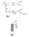
- the deviation from the programmed path over the thickness t of the workpiece in both cases is illustrated in figure 3.
- abscissa the thickness of the workpiece is shown, whereas the deviation from the desired, programmed path 32 is shown in ordinate.
- the curve 34 shows the real path that the wire follows when a mechanical load of 0.2 kg is applied.
- the difference between the desired, programmed path 32 and the obtained path 34 due to first order deviations is indicated by "a”.
- the second order deviations are the highest at the center of the workpiece. These second order deviations at the center of the workpiece are indicated on figure 3 by "b”.
- Curve 36 shows the path that the wire follows when a mechanical load of 1 kg is applied.
- the first order deviations are eliminated by applying a higher mechanical load and the second order deviations, indicated by "d” are reduced with 50 %.
- an EDM wire 40 has a flat or rectangular cross-section.
- This type of wire allows it to combine a high precision and high machining speeds : high machining speeds are obtained because of the heat transfer through the large 'flat' side; while high precision is obtained by cutting with the 'thin' side.
- Flat wires furthermore have the advantage that they can be made very straight which will facilitate (automatic) threading.
- the flat wire 42 has a width of 0.10 mm and a thickness of 0.02 mm.
- a thin Al coating 44 is applied on the wire by cladding or by hot dip.
- the wire is coated with a Zn alloy layer 46 with a thickness of 0.5 ⁇ m.
Landscapes
- Chemical & Material Sciences (AREA)
- Chemical Kinetics & Catalysis (AREA)
- Electrochemistry (AREA)
- Engineering & Computer Science (AREA)
- Mechanical Engineering (AREA)
- Electrical Discharge Machining, Electrochemical Machining, And Combined Machining (AREA)
Abstract
Description
- The invention relates to an electrode for electric discharge machining.
- The process of electrical discharge machining (EDM) is well known : it is a method to cut conductive materials with an electrode wire that follows a programmed path.
- An electrode for EDM has to meet a number of requirements.
In the first place, a good machinability, i.e. a high removal rate, a good surface finish and a high precision, is required.
Furthermore, in order to obtain an automated system, a good threadability is desired.
The machining conditions and the path along which the workpiece is cut, are stored in a control device memory. - During machining, due to the electric discharge, a force with an orientation opposite to the direction in which the machining is proceeding is created on the machining sections of the wire electrode.
As a consequence, the wire lags in the direction in which the machining is proceeding.
Also electrostatic and electromagnetic forces are created on the wire electrode. - Due to all these forces and due to the vibrations of the wire, the actual position of the wire is different from the programmed position. This results in accuracy and precision problems.
This is especially critical for corner cutting. Deviation from the programmed outline at the corners has as result that round corners are obtained in stead of the desired sharp corners.
The deviation between the programmed and the effective outline can be reduced by applying a mechanical load to the wire. - If a high degree of accuracy and precision is desired, the use of wires with a small diameter is desired.
However, since only a limited mechanical load can be applied on the conventional finer wires, such as brass wires, it is difficult to obtain a high degree of accuracy and precision. - Therefore, for example plain Mo or W-wires are used for high precision cutting. These wires have a rather high tensile strength (>1900 MPa) but they have the drawback to be expensive.
Furthermore, since they are characterised by a high melting temperature, they have a low vapor pressure with poor flushability. - It is an object of the present invention to provide an EDM wire electrode having a high tensile strength.
It is also an object to provide an EDM wire electrode which is machining a desired contour with high precision and high accuracy while maintaining a high machining speed.
It is another object to provide an EDM wire electrode which can be manufactured at low costs. - According to a first aspect of the invention, an electrode for electrical discharge machining is provided.
The electrode consists of a high strength pearlitic steel wire having a diameter of 0.35 mm or below.
The steel wire is a high carbon steel wire with a carbon content ranging between 0.6 to 1.2 %. More preferably, the carbon content is higher than 0.7 %.
The wire has a tensile strength higher than 3000 N/mm2, for example 3500 N/mm2 or 4000 N/mm2.
The wire is coated with a copper free zinc or zinc alloy. - Possibly, small traces of copper are present in the zinc or zinc alloy coating layer.
- The pearlitic structure is obtained by heating the steel to a high temperature (900 -1000 °C) at which carbon dissolution and austenitic formation occur, followed by immersion in a quench transformation bath at a temperature between 500 and 700 °C to decompose austenite in a pearlitic structure of desired lamellar fineness.
The patented steel so obtained can be cold deformed; it can for example be drawn or it can be rolled or flattened. - The wire may have a circular or rectangular cross-section. Alternatively, a steel strip may be used.
- If wires with a circular cross-section are used, the diameter is preferably lower than 0.35 mm, and more preferably lower than 0.25 mm, for example 0.1,0.07 or 0.03 mm.
As flat wires, wires with a thickness lower than 0.25 mm, for example 0.1 mm, 0.05 mm or 0.02 mm can be considered. - The high strength pearlitic steel core performs the strength function while the zinc or zinc alloy coating performs the heat dissipation and machining function.
- In principle, any coating technique that results in the application of a coating layer according to this invention can thereby be considered. Preferred methods are electrolysis, hot dip and cladding.
Applying a zinc or zinc alloy coating by means of a hot dip galvanizing bath has as result that an iron-zinc alloy layer is created at the surface of the wire.
For thin coatings preference is given to electrolytic deposition. - The thickness of the zinc or zinc alloy coating has to be chosen in such a way that it dissipates enough energy to avoid thermal load and thus breakage of the steel wire. On the other hand, the thickness has to be chosen so that the coated steel is still strong enough to withstand the imposed mechanical load necessary to obtain the required precision.
The thickness of the zinc or zinc alloy coating is preferably between 0.1 and 20 µm.
For a wire with a diameter of 0.10 mm, the thickness of the coating is preferably between 0.5 and 10 µm and more preferably between 1 and 4 µm. - In one embodiment, the zinc alloy is a zinc aluminium alloy. Such a zinc aluminium alloy preferably comprises between 2 and 10 % Al. Between 0.1 and 0.4 % of a rare earth element such as La and/or Ce can be added.
- Possibly, an intermediate layer is applied between the steel and the zinc or zinc alloy layer.
Such an intermediate layer can be an aluminium or a silver layer or it can comprise alloys thereof.
By applying such an intermediate layer the electrical conductivity of the electrode can be improved. The aluminium layer can for example be applied by cladding or by hot dip.
Also a nickel or nickel alloy layer can be considered as intermediate layer. - In one embodiment of the present invention, the electrode comprises an additional layer on top of the zinc or zinc alloy coating.
This additional layer can for example be obtained by the application of an additional coating layer, by a heat treatment or by a passivation process.
The thickness of the coating layer is for example a few nanometers. - Examples of an additional coating layer are a graphite coating layer, an oxide coating layer such as ZnO, Cr2O3, Al2O3, TiO2, ZrO2 or a conductive layer such as a Ag layer.
According to a second aspect, the use of an electrode according to the present invention for electric discharge machining applications is provided.
The electrode is in particular suitable for applications demanding a high precision and a high accuracy. - According to a further aspect of the invention a method of improving the precision and accuracy of the EDM process by applying a mechanical load to a wire electrode as described above is provided.
This method has a positive influence on the machining speed. Furthermore, applying a mechanical load on the wire may also have a positive influence on the surface finish of the machined workpiece. - The invention will now be described into more detail with reference to the accompanying drawings wherein
- FIGURE 1 shows an embodiment of a round EDM wire;
- FIGURE 2 illustrates the test performed in order to evaluate the precision performance of a wire according to the invention;
- FIGURE 3 shows the deviations from the programmed cutting path;
- and FIGURE 4 shows an embodiment of a flat EDM wire.
- Referring to figure 1, an
EDM wire 10 according to the present invention comprises around steel wire 12 with a diameter of 0.10 mm.
The wire has a pearlitic structure and a tensile strength of 4000 N/mm2. A zinc coating with a thickness of 0.5 µm is applied on the wire by electrolysis or hot dip. - The wire is characterised by a high strength. Therefore a high mechanical load can be applied to the EDM wire without breakage of the wire.
By applying a higher mechanical load on the wire, precision errors due to forces created on the wire and due to vibrations of the wire are reduced or even eliminated. - The EDM wire according to the invention is also suitable for taper cutting.
Cutting angles up to 28° could be achieved without breakage of the electrode wire. The cutting angle is defined as the angle between horizontal plane of the workpiece and the EDM wire. - The precision performance of the above described wire is evaluated by cutting a
workpiece 20 as shown in figure 2. Figure 2 a shows the cross-section of the cutted workpiece. The cutting direction of theEDM wire 22 is indicated by the arrow.
The cutting path comprises a comer α of 60 °.
Figure 2b shows the top-view of the cutted workpiece.
Precision can be evaluated by measuring the deviation from the desired programmed path. - Forces created at the wire electrode during the machining process have as consequence that deviations from the programmed path are observed. These deviations are called first order deviations or profile errors.
Furthermore, second order deviations, also called errors on the wire path, cause a variation over the thickness, t of the workpiece, i.e. a variation between the center and the borders.
These second order deviations are amongst others due to the bending and lagging of the wire during machining. - The cutting performance of the above-described wire is tested when a mechanical load of 0.2 kg and when a mechanical load of 1 kg is applied to the wire.
The deviation from the programmed path over the thickness t of the workpiece in both cases is illustrated in figure 3.
In abscissa, the thickness of the workpiece is shown, whereas the deviation from the desired, programmedpath 32 is shown in ordinate. Thecurve 34 shows the real path that the wire follows when a mechanical load of 0.2 kg is applied.
The difference between the desired, programmedpath 32 and the obtainedpath 34 due to first order deviations is indicated by "a".
The second order deviations are the highest at the center of the workpiece. These second order deviations at the center of the workpiece are indicated on figure 3 by "b".
Curve 36 shows the path that the wire follows when a mechanical load of 1 kg is applied. The first order deviations are eliminated by applying a higher mechanical load and the second order deviations, indicated by "d" are reduced with 50 %. - From figure 3, it can be concluded that applying a higher mechanical load on to wire has a positive influence on both the first and the second order deviations and consequently results in a higher precision and higher accuracy.
- It has been observed that applying a higher mechanical load on the wire may also have a positive influence on the machining speed : the machining speed could be improved with 10 % by increasing the mechanical load on the wire.
Furthermore, the surface finish of the surface can be improved by applying a higher mechanical load due to a more stable process - In another embodiment, as shown in figure 4, an
EDM wire 40 has a flat or rectangular cross-section.
This type of wire allows it to combine a high precision and high machining speeds : high machining speeds are obtained because of the heat transfer through the large 'flat' side; while high precision is obtained by cutting with the 'thin' side.
Flat wires furthermore have the advantage that they can be made very straight which will facilitate (automatic) threading. - The
flat wire 42 has a width of 0.10 mm and a thickness of 0.02 mm.
Athin Al coating 44 is applied on the wire by cladding or by hot dip.
In a subsequent step the wire is coated with aZn alloy layer 46 with a thickness of 0.5 µm.
Claims (10)
- An electrode for electric discharge machining, said electrode comprising a high strength pearlitic steel wire having a carbon content higher than 0.6%, having a diameter of 0.35 mm or below and having a tensile strength higher than 3000 N/mm2, said steel wire being coated with a copper free zinc or zinc alloy coating.
- An electrode according to any one of the preceding claims, wherein said wire has a diameter lower than 0.10 mm.
- An electrode according to any one of the preceding claims, wherein said wire has a flat or rectangular cross-section.
- An electrode according to any one of the preceding claims, wherein an iron-zinc alloy layer is created at the surface of the steel wire.
- An electrode according to any one of the preceding claims wherein the zinc alloy is a zinc aluminium alloy.
- An electrode according to any one of the preceding claims, wherein said electrode has an intermediate layer of aluminium, silver or nickel or of alloys thereof between the steel wire and the zinc or zinc alloy layer.
- An electrode according to any one of the preceding claims, wherein said electrode comprises an additional layer on top of said copper free zinc or zinc alloy coating.
- The use of an electrode according to any one of claims 1 to 7 for electric discharge machining applications.
- The use of an electrode according to claim 8 for high precision performance applications.
- A method of improving the precision and accuracy of the electric discharge machining process by applying a mechanical load to the wire electrode according to any one of claims 1 to 7.
Priority Applications (1)
| Application Number | Priority Date | Filing Date | Title |
|---|---|---|---|
| EP01940341A EP1283757B1 (en) | 2000-05-24 | 2001-04-17 | Electric discharge machining wire |
Applications Claiming Priority (4)
| Application Number | Priority Date | Filing Date | Title |
|---|---|---|---|
| EP00201855 | 2000-05-24 | ||
| EP00201855 | 2000-05-24 | ||
| PCT/EP2001/004371 WO2001089750A1 (en) | 2000-05-24 | 2001-04-17 | Electric discharge machining wire |
| EP01940341A EP1283757B1 (en) | 2000-05-24 | 2001-04-17 | Electric discharge machining wire |
Publications (2)
| Publication Number | Publication Date |
|---|---|
| EP1283757A1 EP1283757A1 (en) | 2003-02-19 |
| EP1283757B1 true EP1283757B1 (en) | 2004-09-08 |
Family
ID=8171549
Family Applications (1)
| Application Number | Title | Priority Date | Filing Date |
|---|---|---|---|
| EP01940341A Expired - Lifetime EP1283757B1 (en) | 2000-05-24 | 2001-04-17 | Electric discharge machining wire |
Country Status (7)
| Country | Link |
|---|---|
| US (1) | US6875943B2 (en) |
| EP (1) | EP1283757B1 (en) |
| AT (1) | ATE275457T1 (en) |
| AU (1) | AU2001273949A1 (en) |
| DE (1) | DE60105410T2 (en) |
| PT (1) | PT1283757E (en) |
| WO (1) | WO2001089750A1 (en) |
Families Citing this family (6)
| Publication number | Priority date | Publication date | Assignee | Title |
|---|---|---|---|---|
| TWI377102B (en) * | 2009-11-18 | 2012-11-21 | Ind Tech Res Inst | Wire cut electrical discharge machine |
| EP2595773A4 (en) * | 2010-07-23 | 2014-03-12 | Innovative Technology Providers Llc | Graphitized edm wire |
| JP2013139073A (en) * | 2012-01-06 | 2013-07-18 | Sumitomo Electric Ind Ltd | Electrode wire for wire electric discharge machining and method of manufacturing the same |
| DE102013009767A1 (en) | 2013-06-11 | 2014-12-11 | Heinrich Stamm Gmbh | Wire electrode for spark erosive cutting of objects |
| CN105081490B (en) * | 2014-04-23 | 2017-09-12 | 北京富纳特创新科技有限公司 | Line cutting electrode silk and wire-electrode cutting device |
| US11511362B2 (en) * | 2019-02-05 | 2022-11-29 | Cap Technologies, Llc | Wire for electric discharge machining |
Family Cites Families (12)
| Publication number | Priority date | Publication date | Assignee | Title |
|---|---|---|---|---|
| US3048497A (en) * | 1958-02-18 | 1962-08-07 | Moller Goran August | Process of coating base metals with aluminum |
| US3885120A (en) * | 1973-07-03 | 1975-05-20 | Us Army | Electrode and flux combination for submerged arc welding |
| GB2015909B (en) * | 1978-03-03 | 1982-12-01 | Charmilles Sa Ateliers | Electrode for spark erosion machining |
| US4422906A (en) * | 1981-09-17 | 1983-12-27 | Masami Kobayashi | Process for direct gold plating of stainless steel |
| JPS59110515A (en) * | 1982-12-17 | 1984-06-26 | Sodeitsuku:Kk | Electrical machining method and device thereof |
| JPS6017044A (en) * | 1983-07-06 | 1985-01-28 | Mitsubishi Electric Corp | Wire electrode for wire-cut electric spark machining |
| GB8600533D0 (en) * | 1986-01-10 | 1986-02-19 | Bekaert Sa Nv | Manufacturing pearlitic steel wire |
| JPS63174717A (en) * | 1987-01-14 | 1988-07-19 | Hitachi Cable Ltd | Manufacturing method of composite wire |
| FR2626290B1 (en) * | 1988-01-25 | 1990-06-01 | Michelin & Cie | METHODS AND DEVICES FOR THERMALLY TREATING CARBON STEEL WIRES TO PROVIDE A FINE PERLITRIC STRUCTURE |
| EP0330752B1 (en) * | 1988-02-29 | 1994-03-02 | Kabushiki Kaisha Kobe Seiko Sho | Superhigh-strength superfine wire, and reinforcing materials and composite materials incorporating the same |
| KR920010862B1 (en) * | 1988-06-30 | 1992-12-19 | 미쯔비시 덴끼 가부시기가이샤 | Wire electrode for wire cut discharge processing |
| DE19635775A1 (en) * | 1996-09-04 | 1998-03-05 | Berkenhoff Gmbh | High strength eroding electrode |
-
2001
- 2001-04-17 EP EP01940341A patent/EP1283757B1/en not_active Expired - Lifetime
- 2001-04-17 DE DE60105410T patent/DE60105410T2/en not_active Expired - Fee Related
- 2001-04-17 AU AU2001273949A patent/AU2001273949A1/en not_active Abandoned
- 2001-04-17 AT AT01940341T patent/ATE275457T1/en not_active IP Right Cessation
- 2001-04-17 US US10/275,281 patent/US6875943B2/en not_active Expired - Fee Related
- 2001-04-17 PT PT01940341T patent/PT1283757E/en unknown
- 2001-04-17 WO PCT/EP2001/004371 patent/WO2001089750A1/en not_active Ceased
Also Published As
| Publication number | Publication date |
|---|---|
| AU2001273949A1 (en) | 2001-12-03 |
| ATE275457T1 (en) | 2004-09-15 |
| DE60105410T2 (en) | 2005-09-22 |
| US20040089636A1 (en) | 2004-05-13 |
| EP1283757A1 (en) | 2003-02-19 |
| WO2001089750A1 (en) | 2001-11-29 |
| PT1283757E (en) | 2005-01-31 |
| US6875943B2 (en) | 2005-04-05 |
| DE60105410D1 (en) | 2004-10-14 |
Similar Documents
| Publication | Publication Date | Title |
|---|---|---|
| EP1009574B1 (en) | Electrode wire for use in electric discharge machining and process for preparing same | |
| KR920007689B1 (en) | Electrode wire for wire discharge machining and its manufacturing method | |
| EP0930131B1 (en) | Method of manufacturing porous electrode wire for electric discharge machining and structure of the electrode wire | |
| CN102239024B (en) | Wire electrode for electric discharge cutting processes | |
| US4935594A (en) | Eroding electrode, in particular a wire electrode for the sparkerosive working | |
| US5196665A (en) | Multi-layer electrode wire and method for producing the same | |
| JP2005512826A5 (en) | ||
| US6875943B2 (en) | Electric discharge machining wire | |
| KR100194245B1 (en) | Wire electrode | |
| US5118572A (en) | Filiform electrode with metal coating for spark erosion | |
| JP6615093B2 (en) | Electrical contact material, method of manufacturing electrical contact material, and terminal | |
| CN105283262B (en) | Wire electrode for the cutting object that discharges | |
| JPS61136733A (en) | Electrode wire for wire-cut spark erosion work and preparation thereof | |
| JP3405069B2 (en) | Electrode wire for electric discharge machining | |
| JP2006159304A (en) | Electrode wire for wire electric discharge machining and its manufacturing method | |
| US8519294B2 (en) | Electric discharge machining wire with optimized surface coating | |
| RU2076363C1 (en) | Method for manufacturing of multiple-conductor superconducting wire using nb*003sn compound | |
| US20070295695A1 (en) | EDM wire | |
| JP4917747B2 (en) | Electrode wire for electric discharge machining | |
| JPH07156021A (en) | Electrode wire for electrical discharge machining | |
| Hamdi | Ibrahem Maher, Ahmed AD Sarhan & | |
| KR100485645B1 (en) | The electrode wire for electrical discharge machining, and manufacturing method of it | |
| JPH01210222A (en) | Wire electrode for electric discharge machining | |
| CN121870189A (en) | Electrode wire for electrical discharge machining | |
| JPH07108488B2 (en) | Method for manufacturing electrode wire for wire electric discharge machining |
Legal Events
| Date | Code | Title | Description |
|---|---|---|---|
| PUAI | Public reference made under article 153(3) epc to a published international application that has entered the european phase |
Free format text: ORIGINAL CODE: 0009012 |
|
| 17P | Request for examination filed |
Effective date: 20021024 |
|
| AK | Designated contracting states |
Designated state(s): AT BE CH CY DE DK ES FI FR GB GR IE IT LI LU MC NL PT SE TR |
|
| AX | Request for extension of the european patent |
Extension state: AL LT LV MK RO SI |
|
| GRAP | Despatch of communication of intention to grant a patent |
Free format text: ORIGINAL CODE: EPIDOSNIGR1 |
|
| GRAS | Grant fee paid |
Free format text: ORIGINAL CODE: EPIDOSNIGR3 |
|
| GRAA | (expected) grant |
Free format text: ORIGINAL CODE: 0009210 |
|
| AK | Designated contracting states |
Kind code of ref document: B1 Designated state(s): AT BE CH CY DE DK ES FI FR GB GR IE IT LI LU MC NL PT SE TR |
|
| PG25 | Lapsed in a contracting state [announced via postgrant information from national office to epo] |
Ref country code: TR Free format text: LAPSE BECAUSE OF FAILURE TO SUBMIT A TRANSLATION OF THE DESCRIPTION OR TO PAY THE FEE WITHIN THE PRESCRIBED TIME-LIMIT Effective date: 20040908 Ref country code: FI Free format text: LAPSE BECAUSE OF FAILURE TO SUBMIT A TRANSLATION OF THE DESCRIPTION OR TO PAY THE FEE WITHIN THE PRESCRIBED TIME-LIMIT Effective date: 20040908 Ref country code: BE Free format text: LAPSE BECAUSE OF FAILURE TO SUBMIT A TRANSLATION OF THE DESCRIPTION OR TO PAY THE FEE WITHIN THE PRESCRIBED TIME-LIMIT Effective date: 20040908 Ref country code: AT Free format text: LAPSE BECAUSE OF FAILURE TO SUBMIT A TRANSLATION OF THE DESCRIPTION OR TO PAY THE FEE WITHIN THE PRESCRIBED TIME-LIMIT Effective date: 20040908 |
|
| REG | Reference to a national code |
Ref country code: GB Ref legal event code: FG4D |
|
| REG | Reference to a national code |
Ref country code: CH Ref legal event code: EP |
|
| REG | Reference to a national code |
Ref country code: IE Ref legal event code: FG4D |
|
| REF | Corresponds to: |
Ref document number: 60105410 Country of ref document: DE Date of ref document: 20041014 Kind code of ref document: P |
|
| PG25 | Lapsed in a contracting state [announced via postgrant information from national office to epo] |
Ref country code: SE Free format text: LAPSE BECAUSE OF FAILURE TO SUBMIT A TRANSLATION OF THE DESCRIPTION OR TO PAY THE FEE WITHIN THE PRESCRIBED TIME-LIMIT Effective date: 20041208 Ref country code: GR Free format text: LAPSE BECAUSE OF FAILURE TO SUBMIT A TRANSLATION OF THE DESCRIPTION OR TO PAY THE FEE WITHIN THE PRESCRIBED TIME-LIMIT Effective date: 20041208 Ref country code: DK Free format text: LAPSE BECAUSE OF FAILURE TO SUBMIT A TRANSLATION OF THE DESCRIPTION OR TO PAY THE FEE WITHIN THE PRESCRIBED TIME-LIMIT Effective date: 20041208 |
|
| PG25 | Lapsed in a contracting state [announced via postgrant information from national office to epo] |
Ref country code: ES Free format text: LAPSE BECAUSE OF FAILURE TO SUBMIT A TRANSLATION OF THE DESCRIPTION OR TO PAY THE FEE WITHIN THE PRESCRIBED TIME-LIMIT Effective date: 20041219 |
|
| REG | Reference to a national code |
Ref country code: PT Ref legal event code: SC4A Effective date: 20041112 |
|
| LTIE | Lt: invalidation of european patent or patent extension |
Effective date: 20040908 |
|
| PG25 | Lapsed in a contracting state [announced via postgrant information from national office to epo] |
Ref country code: LU Free format text: LAPSE BECAUSE OF NON-PAYMENT OF DUE FEES Effective date: 20050417 Ref country code: GB Free format text: LAPSE BECAUSE OF NON-PAYMENT OF DUE FEES Effective date: 20050417 Ref country code: CY Free format text: LAPSE BECAUSE OF FAILURE TO SUBMIT A TRANSLATION OF THE DESCRIPTION OR TO PAY THE FEE WITHIN THE PRESCRIBED TIME-LIMIT Effective date: 20050417 |
|
| PG25 | Lapsed in a contracting state [announced via postgrant information from national office to epo] |
Ref country code: IE Free format text: LAPSE BECAUSE OF NON-PAYMENT OF DUE FEES Effective date: 20050418 |
|
| PG25 | Lapsed in a contracting state [announced via postgrant information from national office to epo] |
Ref country code: MC Free format text: LAPSE BECAUSE OF NON-PAYMENT OF DUE FEES Effective date: 20050430 |
|
| ET | Fr: translation filed | ||
| PLBE | No opposition filed within time limit |
Free format text: ORIGINAL CODE: 0009261 |
|
| STAA | Information on the status of an ep patent application or granted ep patent |
Free format text: STATUS: NO OPPOSITION FILED WITHIN TIME LIMIT |
|
| 26N | No opposition filed |
Effective date: 20050609 |
|
| GBPC | Gb: european patent ceased through non-payment of renewal fee |
Effective date: 20050417 |
|
| PGFP | Annual fee paid to national office [announced via postgrant information from national office to epo] |
Ref country code: DE Payment date: 20060308 Year of fee payment: 6 |
|
| PGFP | Annual fee paid to national office [announced via postgrant information from national office to epo] |
Ref country code: FR Payment date: 20060309 Year of fee payment: 6 |
|
| PGFP | Annual fee paid to national office [announced via postgrant information from national office to epo] |
Ref country code: NL Payment date: 20060310 Year of fee payment: 6 |
|
| PGFP | Annual fee paid to national office [announced via postgrant information from national office to epo] |
Ref country code: CH Payment date: 20060313 Year of fee payment: 6 |
|
| PGFP | Annual fee paid to national office [announced via postgrant information from national office to epo] |
Ref country code: PT Payment date: 20060404 Year of fee payment: 6 |
|
| PGFP | Annual fee paid to national office [announced via postgrant information from national office to epo] |
Ref country code: IT Payment date: 20060430 Year of fee payment: 6 |
|
| REG | Reference to a national code |
Ref country code: PT Ref legal event code: MM4A Free format text: LAPSE DUE TO NON-PAYMENT OF FEES Effective date: 20071017 |
|
| REG | Reference to a national code |
Ref country code: CH Ref legal event code: PL |
|
| NLV4 | Nl: lapsed or anulled due to non-payment of the annual fee |
Effective date: 20071101 |
|
| PG25 | Lapsed in a contracting state [announced via postgrant information from national office to epo] |
Ref country code: PT Free format text: LAPSE BECAUSE OF NON-PAYMENT OF DUE FEES Effective date: 20071017 Ref country code: NL Free format text: LAPSE BECAUSE OF NON-PAYMENT OF DUE FEES Effective date: 20071101 Ref country code: DE Free format text: LAPSE BECAUSE OF NON-PAYMENT OF DUE FEES Effective date: 20071101 |
|
| PG25 | Lapsed in a contracting state [announced via postgrant information from national office to epo] |
Ref country code: CH Free format text: LAPSE BECAUSE OF NON-PAYMENT OF DUE FEES Effective date: 20070430 Ref country code: LI Free format text: LAPSE BECAUSE OF NON-PAYMENT OF DUE FEES Effective date: 20070430 |
|
| PG25 | Lapsed in a contracting state [announced via postgrant information from national office to epo] |
Ref country code: FR Free format text: LAPSE BECAUSE OF NON-PAYMENT OF DUE FEES Effective date: 20070430 |
|
| PG25 | Lapsed in a contracting state [announced via postgrant information from national office to epo] |
Ref country code: IT Free format text: LAPSE BECAUSE OF NON-PAYMENT OF DUE FEES Effective date: 20070417 |