Technical field
The invention refers to a charge/discharge protection circuit for a
rechargeable battery comprising at least one rechargeable cell, with a control
logic which opens or closes a load current switch depending on the magnitude of
the voltage at the battery terminals, the voltage at the charge/discharge terminals
of the protection circuit, and the charge or discharge current.
Background art
Where that control logic comprises an over-voltage detector which
produces a control signal when reaching a voltage limit which depends on the
electric strength as determined by the protection circuit. This control signal closes
a short-circuit switch which connects the battery terminals via a load current
switch in series with a fusible link.
Such a circuit is deemed known from the this-side DE-A-101 03 3362,
which is expressly referenced herewith. In particular, this circuit can be disposed
between a single lithium-ion cell and the electronics of a mobile phone. It can be
produced at favorable cost with a significantly lower electric strength than
inherently required in a worst case, because the short-circuit switch closes when
reaching an appropriately determined voltage limit. The resulting short circuit
current thus safely destroys the fusible link so that the cell is protected from a
dangerous overcharge. In contrast to all other circuit elements however, the
fusible link cannot be integrated, or only at high cost, on an IC because it has to
respond very reliably at a tightly toleranced nominal current.
Summary of the invention
It is an object of the present invention to create a protection circuit of the
above described type which can be integrated on a single chip including the
fusible link.
This object is achieved by designing a series circuit comprising the load
current switch and the fusible link for a fraction 1/n of the nominal current and
shunting n of such series circuits in parallel, that the short-circuit switch consists
of n switch segments, each of which coupled between the node of the load current
switch and the fusible link of the series circuit x (x = 1, 2...n) and the opposite
battery connection, that the over-voltage detector creates in sequential
succession for each switch segment x a separate control signal, and that there is
disposed a semiconductor switch in parallel to the charge/discharge terminals of
the protection circuit, which the over-voltage detector switches conductively when
reaching the predetermined voltage limit.
The central idea of the invention is, therefore, to create the condition where
the fuse segments in the case of an over-voltage are reliably destroyed and where
the destruction proceeds sequentially from the first to the last fuse segment. This
is achieved by dividing the functions of the load current switch, the fusible link,
and the short-circuit switch into in parallel arranged T-sections, each of which is
designed for only a fraction of the nominal load so that each of the easily
integrated fuse segments carry only the respective fraction of the nominal current.
It is important in this case that the entire protection circuit or its control logic will
not be destroyed before through that unduly high over-voltage, in which case the
sequential blowing of the fuse segments would no longer be guaranteed. This is
taken care of by the semiconductor switch which immediately short-circuits a
recognized over-voltage.
Appropriately, the over-voltage detector receives as input voltage the
voltage at the charge/discharge terminals. In principle, the over-voltage detector
could also receive as input voltage the voltage via the parallel circuit of the
opened load current switches, the load current switches having opened due to the
over-current caused by the previous over-voltage.
Appropriately, at least those circuit components of the control logic
generating the control signals for the switch segments receive their supply voltage
from an auxiliary voltage source, in particular from a charged buffer capacitor.
This safeguards the function of the protection circuit when the outer over-voltage
is short-circuited by the semiconductor switch or if it is so high that it has lead to a
destruction of other intended parts of the control logic.
The over-voltage detector may in particular comprise a bistable flip-flop
circuit, which switches to its second stable state when the predetermined voltage
limit is reached, so that the sequential closing of the switch segments of the short-circuit
switch is initiated when the predetermined voltage limit is reached during
even briefly.
The over-voltage detector may comprise a clock generator followed by a
shift register of at least n levels, which, when reaching the predetermined voltage
limit, delivers sequentially the control signals for the switch segments of the short-circuit
switch.
Alternatively to this method of producing the control signals, it is possible
that each switch segment of the short-circuit switch has associated with it a
voltage detector, which delivers a signal at its output when the voltage at this
switch segment disappears as a result of the blowing of the associated fuse
segment whereby the outputs of the voltage detectors are coupled to a logic
circuit which comprises a clock generator and which, when exceeding the voltage
limit, produces the control signal for the next in line switch segment only when the
voltage detector of the preceding switch segment delivers an output signal. The
logic circuit can be realized, in particular, with an appropriate number of
sequentially connected and with each other coupled flip-flops, as is well
understood by those skilled in the art, or an appropriate number of short shift
registers. Utilizing shift registers has the advantage in this instance that the
control signals do not follow each other immediately, but have a short delay
determined by the frequency of the clock generator and the number of shift
register stages, thus allowing the current path created by the prior blowing of the
fuse segment to cool down.
In particular, the semiconductor switch and/or the switch segments of the
short-circuit switch may comprise two in series connected, parallel controlled
single switches, in order that these components may also be realized in a low-cost
technology offering only low electric strength.
Preferably, all circuit components, with the exception of capacitors, are
integrated on a chip.
Description of the drawings
Embodiments of a protection circuit according to the present invention are
shown schematically simplified in the drawings. Illustrated is:
Description of the preferred embodiment
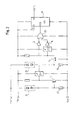
The protection circuit illustrated in Figure 1 is located as an integrated
circuit between the terminals of a Li-Ion cell 1 and two charge/ discharge terminals
50 and 60, paralleled to which is a filter-capacitor 40 as protection against steeply
sloped voltage increases. The protection circuit has the outer connections Com,
+Batt and Out as well as +VH. The latter is connected via a buffer capacitor 2 with
the reference potential Com. Buffer capacitor 2 is normally charged to the battery
voltage via semiconductor switch 4 (indicated as a diode). If this supply voltage
drops away then semiconductor switch 4 opens and the buffer capacitor 2
supplies, via line 5, power for a time for essential parts of the integrated circuit. A
charge pump circuit may also be used in place of semiconductor switch 4, where
the charge pump circuit charges the buffer capacitor 2 to the intended maximum
gate voltage as dictated by the technology of the integrated circuit.
A current sensing resistor Rsense is placed between Out and +Batt in series
with a circuit arrangement, which comprises a plurality of parallel coupled series
circuits, in turn each comprising a load current switch 101, 102,... 10n and an
integrated fusible link 111, 112,... 11n. Each connection node between a load
current switch 10x and a fusible link 11x is connected to the reference potential
Com via its own short-circuit switch 121, 122,... 12n.
A control logic, pictured in simplified form within dash-dotted block 6,
generates by generally known means through differential amplifiers D1 and D2 a
battery under-voltage signal UV and a battery over-voltage signal OV, provided
the voltage of the Li-Ion cell is outside of the predetermined tolerance range. The
control logic further generates from the voltage drop across Rsense by means of
differential amplifiers D3, D4 the output signals OCD, OCC, respectively, when
reaching the maximum charge current or the maximum discharge current,
respectively. Output signals UV, OV, OCC and OCD of differential amplifiers D1
to D4 are coupled into OR-gate OD which supplies an output signal F1 which
opens in each of the mentioned cases all load current switches 101 through 10n.
The voltage Vout is applied at the same time to the input of an over-voltage
detector OVD which generates an error signal F2 in case of an over-voltage.
Error signal F2 also closes at the same time two semiconductor switches 7, 8
which are connected in series between Com and Out, generates via OR-gate OD
the error signal F1 to open the load current switches 101 through 10n, and
activates a clock generator CLK. Coupled to the clock generator CLK is a shift
register SR which then sequentially delivers error signals F3 [1:n] for successive
closing of the short-circuit switches 121 through 12n. This has the consequence
that, one after the other, fuses 111 through 11n blow, so that Li-Ion cell 1 will be
cut off from Out after a few milliseconds to a few 100 milliseconds. At least until
the last fuse 11n has blown, control logic 6 will be fed by the buffer capacitor 2, if
necessary.
Figure 2 illustrates an embodiment of the over-voltage detector. The
designations of the outer connections correspond with those of Figure 1. Placed
between Out and Com is a series circuit comprising first trigger element 21 and a
resistor 22 as well as a second trigger element 23 and a second resistor 24.
Trigger elements 21, 23 are only illustrated symbolically as the series connection
of a zener diode and a back current diode wired back-to-back. When exceeding
the predetermined voltage limit in the positive or negative direction the
corresponding trigger element becomes conductive and with it the respective,
following MOS transistor T1 or T2, which in turn sets to A0" or AL@ the following
Schmitt-Trigger ST1, ST2, respectively. The outputs of the Schmitt-Triggers are
coupled via Inverter I with the inputs of a NAND-gate 25, whose output in turn is
connected with the clock input of a D flip-flop 26. Its D-input is normally at A1" or
AH@. The output Q of flip-flop 26, therefore, goes to AH@ when at the clock
input an impulse arrives from OR-gate 25. The over-voltage detector behaves,
therefore, like a bistable flip-flop. The output signal AH@ represents the signal
F2.
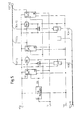
Figure 3 illustrates clock generator CLK with the shift register SR coupled
to it as shown in Figure 1. Clock generator CLK is started when signal F2 is
applied to its start input EN and supplies at its output clock pulses clk, which are
applied to the clock input of shift register SR. At the same time the latter receives
at its signal input XR the signal F2 and at its D-input the signal A1" or AH@. Shift
register SR outputs Q1, Q2, ... Qn, equal to signal F3 [1:n], thus switch sequentially
from AL@ to AH@ in accordance with the clock signal, thereby delivering
sequentially following control signals for closing of the switch segments 121
through 12n in Figure 1.
Figure 4 illustrates a block diagram of a second embodiment of the
protection circuit. Having a similar arrangement as the embodiment of Fig. 1, it
differs from that because voltages V1 through Vn-1 picked off at the short-circuit
switches 121 through 12n are selected and then supplied to a logic circuit LS,
replacing the shift register SR of Fig. 1.
This logic circuit LS supplies sequentially the control signals F3 [1:n] and is
illustrated in Fig. 5. It receives those in Fig. 4 named voltages or signals and
includes for each switch segment 121 through 12n, respectively the voltages V1
through Vn-1 picked off from each, a voltage detector ST illustrated as a Schmitt-Trigger,
and a number of D-flip-flops DFF1 through DFFn whose number equals
the number of switch elements. The clock generator CLK, preferably operating at
a higher frequency than the one of Fig. 1, will be started by signal F2 as before
and delivers clock signals clk to the clock input of DFF1. Because error signal F2
is applied at the same time to all inputs XR of the D-flip-flops, thereby enabling
them, the first clock pulse CLK forces output Q of DFF1 to A1" and thereby
generates the first control signal F3 [1] which closes switch segment 121. As long
as its own fuse segment 111 is still intact, the voltage V1 is then > 0 V (typically 0.5
to 1.5 V). The corresponding voltage detector therefore supplies an output signal
A1". When fuse 111 has blown a short time after the closing of the switch
segment then the voltage switches to V1 < 0.5 V. The output signal of the voltage
detector goes to A0". The following inverter I generates out of it a A1" for the
second input of AND-gate U1. Applied to the first input is signal F3 [1], so that the
output of the AND-gate U1 also switches to A1A. This output is coupled to the D-input
of the next flip-flop DFF2, which, in corresponding manner, supplies with the
next rise of the clock signal clk the control signal F3 [2] etc..
A further improvement (but not illustrated in the drawings) consists of
replacing each of the flip-flops DFF by a short shift register, e.g. with three
successive, appropriately coupled D-flip-flops. Thus, each control signal will be
generated after a time delay of e.g. three clock cycles, after the voltage Vx at the
respective switch element has dropped, due to the blowing of the respective fuse
element, below the switching threshold of the voltage detector. During this time
delay the current path of the just- before blown fuse element can cool down. This
method avoids having a retroactive effect on the response characteristics of the
physically closely spaced adjacent, and still intact, fuse element.
Should, in the meantime, the current path of this fuse element become
again conductive when the before melted-away metal ,typically aluminum,
solidifies, then this would be recognized by its own voltage detector in the same
manner as before and a new blowing of this fuse element would be initiated. This
further increases the reliability of the protection function of the total circuit.