EP1280277A2 - Calibration of isolated analog-to-digital converters - Google Patents
Calibration of isolated analog-to-digital converters Download PDFInfo
- Publication number
- EP1280277A2 EP1280277A2 EP02013901A EP02013901A EP1280277A2 EP 1280277 A2 EP1280277 A2 EP 1280277A2 EP 02013901 A EP02013901 A EP 02013901A EP 02013901 A EP02013901 A EP 02013901A EP 1280277 A2 EP1280277 A2 EP 1280277A2
- Authority
- EP
- European Patent Office
- Prior art keywords
- analog
- isolated
- digital converters
- digital
- converter system
- Prior art date
- Legal status (The legal status is an assumption and is not a legal conclusion. Google has not performed a legal analysis and makes no representation as to the accuracy of the status listed.)
- Granted
Links
Images



Classifications
-
- H—ELECTRICITY
- H03—ELECTRONIC CIRCUITRY
- H03M—CODING; DECODING; CODE CONVERSION IN GENERAL
- H03M1/00—Analogue/digital conversion; Digital/analogue conversion
- H03M1/10—Calibration or testing
- H03M1/1009—Calibration
- H03M1/1028—Calibration at two points of the transfer characteristic, i.e. by adjusting two reference values, e.g. offset and gain error
-
- H—ELECTRICITY
- H03—ELECTRONIC CIRCUITRY
- H03M—CODING; DECODING; CODE CONVERSION IN GENERAL
- H03M1/00—Analogue/digital conversion; Digital/analogue conversion
- H03M1/06—Continuously compensating for, or preventing, undesired influence of physical parameters
- H03M1/08—Continuously compensating for, or preventing, undesired influence of physical parameters of noise
- H03M1/0827—Continuously compensating for, or preventing, undesired influence of physical parameters of noise of electromagnetic or electrostatic field noise, e.g. preventing crosstalk by shielding or optical isolation
-
- H—ELECTRICITY
- H03—ELECTRONIC CIRCUITRY
- H03M—CODING; DECODING; CODE CONVERSION IN GENERAL
- H03M1/00—Analogue/digital conversion; Digital/analogue conversion
- H03M1/12—Analogue/digital converters
Definitions
- the present invention relates to analog-to-digital converters.
- the present invention is directed toward calibration of isolated analog-to-digital converters.
- Measurement data collected by isolated analog-to-digital converters (ADCs) in multiple data channels may be related. Data from the isolated ADCs may be transmitted to a microcontroller or programmable logic device for centralized processing. The gain and offset of individual channels relative to one another is an issue which may require attention. Such applications are precise, cost-sensitive applications where providing each ADC with a precise reference is not an affordable solution.
- ADCs analog-to-digital converters
- ADCs are known to need isolation in applications subject to different voltage levels.
- the reference voltage of an ADC is not necessarily the same as the reference voltage, which would be observed by an outside observer (e.g., relative to absolute ground).
- the recording equipment processor used with an ADC may work with another power supply, and the various power supplies may be very different both in voltage levels and in power supply characteristics.
- a ground line and a live line there may be provided a ground line and a live line.
- the live line may have a potential, for example, 220 Volts from the neutral line.
- the ADC front end in order to make a measurement on the ground or neutral line and simultaneously make a measurement on the live line, the ADC front end must be able to accommodate vastly different voltage levels (i.e., the voltage reference to the live line, such as 220 Volts absolute and a ground reference).
- the measurement device and the data processor may need to be isolated electrically from one another.
- isolation capacitors as an isolation barrier in multi-link systems.
- a transformer or other isolation device may also be used to isolate the ADC from the microcontroller or programmable logic device.
- isolation barriers may make it difficult to calibrate the ADC since the microcontroller or programmable logic device may have difficulty sending a precise voltage reference signal through the isolation barrier.
- FIG. 1 is a block diagram of a measurement system 9 of the prior art.
- Such measurement systems may be used to measure various analog parameters in environments where voltage isolation is required.
- a measurement device front end
- line voltage e.g. 220 Volts
- some form of isolation may be required to protect the user and processor (back end) which may be at a much lower potential.
- voltage isolation may be required as a fail-safe to prevent a patient from being electrocuted due to potential differences between various medical monitoring devices connected to a patient.
- measurement system 9 may include a digital signal processor (DSP) 11, link chip 12, capacitor C1 13, analog-to-digital converter (ADC) and link chip 15, and a sensor 16.
- DSP digital signal processor
- ADC analog-to-digital converter
- Sensor 16 may comprise any one of a number of known analog sensors for measuring a particular parameter (e.g., temperature, pressure, voltage, amperage, power consumption, or the like).
- Analog-to-digital converter (ADC) and link chip 15 may convert the analog output of sensor 16 to a digital value (typically a one-bit data stream) and outputs this data stream to a digital signal processor (DSP) 11 via link chip 12 and isolation capacitor 13.
- DSP digital signal processor
- ADC analog-to-digital converter
- other signals may need to be exchanged between the two chips.
- clock signals and control signals may be transmitted from digital signal processor (DSP) 11 to analog-to-digital converter (ADC) through link chip 15.
- digital signal processor (DSP) 11 may need to provide power supply voltage to analog-to-digital converter through link chip 15.
- additional signal lines may be required for such additional signals, increasing the complexity and cost of the device.
- ADC analog-to-digital converter
- DSP digital signal processor
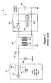
- FIG. 2 is a block diagram of another embodiment of a measurement system 19 of the prior art.
- Measurement system 19 includes a digital application specific integrated circuit (ASIC) or programmable logic device (PLD) 21 such as a digital signal processor and link chip, a resistor 22, capacitor 23, transformer 24, analog-to-digital converter (ADC) 25 and capacitor 26.
- ASIC application specific integrated circuit
- PLD programmable logic device
- ASIC or PLD 21 may include a transmitter 27 and receiver 29 coupled to each other through switch 28. Data may be selectively transmitted and received over the connection between ASIC or PLD 21 and ADC 25. In addition, ASIC or PLD 21 may provide power to ADC 25 through this same link.
- ADC 25 may include a diode 30 and a rectifier 31. Signals from secondary winding 33 of transformer 24 may be rectified by rectifier 31 and diode 30 to produce a voltage for a capacitor 26 which in turn is the power supply for ADC 25.
- transmitter 27 may transmit to primary winding 32 of transformer 24 a square wave, which may be partially blocked or distorted by capacitor 23 from transformer 24.
- ADC 25 may detect a pause during the tri-state operation and takes over the data link, sending data and status back to receiver 29. During this take-over period, however, voltage at power supply 26 may droop significantly if many bits are transmitted, and full logic levels may not re-establish themselves.
- an isolated ADC may require an accurate low noise reference voltage from, for example, a microcontroller. If the ADC is rendered in CMOS, a superquality voltage reference may be required for the ADC to accurately measure analog values. CMOS circuitry may be more susceptible to drift due to temperature variations and the like, as well as initial accuracy of measurement.
- CMOS circuitry may be more susceptible to drift due to temperature variations and the like, as well as initial accuracy of measurement. A better reference, therefore, may be implemented on the isolated side.
- Related measurement data collected by isolated analog-to-digital converters in multiple channels may be transmitted to a microprocessor or programmable logic device for centralized processing to eliminate selected gain and offset effects common to the different analog-to-digital converters in the different channels, eliminating the consequences of drift in the different channels.
- a pair of precision resistors is provided to calibrate the different channels.
- the ADCs may be factory calibrated, and the ratio between the two precision resistors may be stored within the ADCs.
- the ADCs may later self-calibrate by comparing their relative gains to the stored resistor ratio. Gain of one of the ADCs may be adjusted relative to the other in order to maintain a relative gain calibration.
- absolute gain is not calibrated (as the resistors are isolated) for particular applications, only relative gain between the ADCs is relevant.
- the present invention provides a cost-effective and simple solution to relative gain calibration between isolated ADCs.
- the system employs first and second sensors for receiving respective first and second analog signals.
- the signals from the respective sensors may be converted with respective first and second analog-to-digital converters into counterpart digital signals.
- Corresponding first and second transformers couple the separate signal streams into a data processing system connected to the first and second transformers, whereby the transformers isolate the data processing systems from the respective analog-to-digital converters.
- First and second analog-to-digital converters may be referenced to respective local grounds, which may be at very different potentials.
- the respective analog-to-digital converters may employ on-chip CMOS bandgap references. These references have relatively high temperature drift and time drift characteristics. Such references may be calibrated with precisely matched inputs from the first and second resistors.
- the resistors may be manufactured on a common substrate, which features good thermal conduction and electrical insulation characteristics. Chips comprising ADC may be provided with silicon thermal meters. The apparatus may then be subject to a two-temperature factory calibration. The ratio variation of the first and second resistors over temperature and time may be less than 100 ppm.
- first and second resistors carry substantially the same current and the ADCs do not draw much current from the first and second resistors, a pair of ratio matched voltages is established with the first and second resistors for the calibration of the CMOS bandgap references in the respective ADCs to the aforementioned desired accuracy level.
- FIG. 3 there is shown a block diagram of a two channel isolated analog-to-digital converter system 139, wherein the analog-to-digital converters 143 and 153 are isolated from the microprocessor or programmable logic device 141 by first and second transformers 142 and 152, respectively.
- System 139 includes a microprocessor or programmable logic device 141 which is coupled to first and second analog-to-digital converters 143 and 153 through respective first and second transformers 142 and 152.
- a current limiting/isolating resistor R L 145 may limit overall current and isolate the two calibration resistors R 1 144 and R 2 146 from one another.
- First and second calibration resistors R 1 144 and R 2 146 may be coupled to the outputs of analog-to-digital converters 143 and 153, respectively.
- First and second analog-to-digital converters 143, and 153 may be referenced to respective local grounds GND1 and GND2, which may be at very different potentials.
- the respective analog-to-digital converters 143 and 153 may employ on-chip CMOS bandgap references. These references have relatively high temperature drift and time drift characteristics. Such references may be calibrated with precisely matched inputs from first and second resistors 144 and 146.
- Resistors 144 and 146 may be manufactured on a common substrate, which features good thermal conduction and electrical insulation characteristics. Chips comprising ADCs 143 and 153 may be provided with silicon thermal meters. The apparatus may then be subject to a two-temperature factory calibration. The ratio variation of the first and second resistors over temperature and time may be less than 100 ppm.
- first and second resistors carry substantially the same current, with the ADCs not drawing much current from the first and second resistors, a pair of ratio matched voltages is established with the first and second resistors for the calibration of the CMOS bandgap references in the respective ADCs to the aforementioned desired accuracy level.
- a low cost alternative for calibrating isolated ADCs in multiple gain channels using multiple precise references is provided.
- the present invention has particular application in instances where multiple ADCs must have precisely matched gains.
- An example of this is a residual current device which is designed to detect a small difference between two almost equally large currents in the "line" (e.g., hot) and neutral wires in an AC power circuit (e.g., ground fault detection and the like).
- the gains of the ADCs may need to be closely matched, although the absolute gains of the ADCs may not need to be so accurate.
- each ADC may be periodically gain-calibrated with matched inputs from the pair of matched precision resistors R 1 and R 2 as set forth above. The relative gains of the two ADCs will thus be closely matched to one another, while the absolute gain may be less relevant.
- the gains of the two ADCs are known.
- the two ADCs measure and record the ratio of R 1 /R 2 .
- the ratio of R 1 /R 2 is assumed to be unchanged while the gains of the ADCs may have drifted.
- the ADCs measure the ratio R 1 /R 2 again, and any changes in the result is attributed to the gain drift of the ADCs.
- one of the ADCs e.g., ADC2
- ADC2 is the one that has drifted, and its gain may then be calibrated to match the other ADC. Again, relative gain of one ADC to another may be more important than absolute gain.
- FIG. 4 is a block diagram of a two channel isolated analog-to-digital converter system of the present invention illustrated in a power metering application.
- ADC 143 may measure current through "HOT" 220VAC line 420, for example, by measuring a voltage drop across resistor 440.
- ADC 153 may measure current through "NEUTRAL 220VAC line 410, for example, by measuring a voltage drop across resistor 430.
- any difference in detected current can be measured as a ground fault, for example.
- the absolute gain of the ADCs is irrelevant in such an application, only the relative gains need be precisely matched.
- ADC 143 may be tied to "HOT" 220VAC line 420 as a reference "ground”
- ADC 153 may be tied to "NEUTRAL" 220VAC line 410.
- each of ADCs 143, 153 are tied to disparate ground levels. The present invention allows for relative calibration between the ADCs despite the different grounding levels of the ADCs.
- the invention described herein may be readily extended to more than two ADCs, where one ADC could be assumed to have no gain drift, and all others gain-calibrated with that ADC.
- n ADCs n-1 pairs of precision resistors may be provided.
Landscapes
- Engineering & Computer Science (AREA)
- Theoretical Computer Science (AREA)
- Analogue/Digital Conversion (AREA)
- Semiconductor Integrated Circuits (AREA)
Abstract
Description
- The present invention relates to analog-to-digital converters. In particular, the present invention is directed toward calibration of isolated analog-to-digital converters.
- Measurement data collected by isolated analog-to-digital converters (ADCs) in multiple data channels may be related. Data from the isolated ADCs may be transmitted to a microcontroller or programmable logic device for centralized processing. The gain and offset of individual channels relative to one another is an issue which may require attention. Such applications are precise, cost-sensitive applications where providing each ADC with a precise reference is not an affordable solution.
- ADCs are known to need isolation in applications subject to different voltage levels. The reference voltage of an ADC is not necessarily the same as the reference voltage, which would be observed by an outside observer (e.g., relative to absolute ground). Moreover, the recording equipment processor used with an ADC may work with another power supply, and the various power supplies may be very different both in voltage levels and in power supply characteristics.
- For example, in a power meter chip used to measure power consumption (e.g., in a residential or business metering or measuring system) with one or three phases, there may be provided a ground line and a live line. The live line may have a potential, for example, 220 Volts from the neutral line. Thus, in order to make a measurement on the ground or neutral line and simultaneously make a measurement on the live line, the ADC front end must be able to accommodate vastly different voltage levels (i.e., the voltage reference to the live line, such as 220 Volts absolute and a ground reference). The measurement device and the data processor may need to be isolated electrically from one another.
- It is known in the art to use isolation capacitors as an isolation barrier in multi-link systems. A transformer or other isolation device may also be used to isolate the ADC from the microcontroller or programmable logic device. However, such isolation barriers may make it difficult to calibrate the ADC since the microcontroller or programmable logic device may have difficulty sending a precise voltage reference signal through the isolation barrier.
- Figure 1 is a block diagram of a
measurement system 9 of the prior art. Such measurement systems may be used to measure various analog parameters in environments where voltage isolation is required. For example, in residential power metering, a measurement device (front end) may be measuring power at line voltage (e.g., 220 Volts) and some form of isolation may be required to protect the user and processor (back end) which may be at a much lower potential. Similarly, in medical systems, voltage isolation may be required as a fail-safe to prevent a patient from being electrocuted due to potential differences between various medical monitoring devices connected to a patient. - Referring to Figure 1,
measurement system 9 may include a digital signal processor (DSP) 11,link chip 12,capacitor C1 13, analog-to-digital converter (ADC) andlink chip 15, and asensor 16.Sensor 16 may comprise any one of a number of known analog sensors for measuring a particular parameter (e.g., temperature, pressure, voltage, amperage, power consumption, or the like). - Analog-to-digital converter (ADC) and
link chip 15 may convert the analog output ofsensor 16 to a digital value (typically a one-bit data stream) and outputs this data stream to a digital signal processor (DSP) 11 vialink chip 12 andisolation capacitor 13. In addition to digital data values transmitted from analog-to-digital converter (ADC) andlink chip 15 to digital signal processor (DSP) 11, other signals may need to be exchanged between the two chips. - For example, clock signals and control signals (including calibration signals or voltage levels) may be transmitted from digital signal processor (DSP) 11 to analog-to-digital converter (ADC) through
link chip 15. In addition, digital signal processor (DSP) 11 may need to provide power supply voltage to analog-to-digital converter throughlink chip 15. In the prior art, additional signal lines may be required for such additional signals, increasing the complexity and cost of the device. - In many applications, it may be necessary to isolate analog-to-digital converter (ADC) from
link chip 15 and digital signal processor (DSP) 11 due to differences in voltage potential. Anisolation capacitor 13 may be employed to isolate the voltage potential between analog-to-digital converter andlink chip 15 and digital signal processor (DSP) 11. - Figure 2 is a block diagram of another embodiment of a measurement system 19 of the prior art. Measurement system 19 includes a digital application specific integrated circuit (ASIC) or programmable logic device (PLD) 21 such as a digital signal processor and link chip, a
resistor 22,capacitor 23,transformer 24, analog-to-digital converter (ADC) 25 andcapacitor 26. - ASIC or PLD 21 may include a
transmitter 27 andreceiver 29 coupled to each other throughswitch 28. Data may be selectively transmitted and received over the connection between ASIC or PLD 21 andADC 25. In addition, ASIC or PLD 21 may provide power to ADC 25 through this same link. - ADC 25 may include a
diode 30 and arectifier 31. Signals fromsecondary winding 33 oftransformer 24 may be rectified byrectifier 31 anddiode 30 to produce a voltage for acapacitor 26 which in turn is the power supply forADC 25. - As in the embodiment of Figure 1,
transmitter 27 may transmit toprimary winding 32 of transformer 24 a square wave, which may be partially blocked or distorted bycapacitor 23 fromtransformer 24. ADC 25 may detect a pause during the tri-state operation and takes over the data link, sending data and status back toreceiver 29. During this take-over period, however, voltage atpower supply 26 may droop significantly if many bits are transmitted, and full logic levels may not re-establish themselves. - In addition, an isolated ADC may require an accurate low noise reference voltage from, for example, a microcontroller. If the ADC is rendered in CMOS, a superquality voltage reference may be required for the ADC to accurately measure analog values. CMOS circuitry may be more susceptible to drift due to temperature variations and the like, as well as initial accuracy of measurement.
- Further, in order to perform an absolutely accurate conversion with an isolated ADC, it may be necessary to send an accurate low noise reference voltage across the isolation barrier. If the ADC is rendered in CMOS, a superquality voltage reference may be required for the ADC to accurately measure analog values. CMOS circuitry may be more susceptible to drift due to temperature variations and the like, as well as initial accuracy of measurement. A better reference, therefore, may be implemented on the isolated side.
- Moreover, in some applications, it may be necessary to provide multiple isolated ADCs with precisely matched gains for acquiring related signals such that conversion data are known to be exactly at the same scale. These may be ratiometric measurements between several isolated points. Prior art techniques may use separate chips for each ADC side to provide a reference signal. However, such a solution creates extra cost and increases complexity and size of the overall circuitry.
- Related measurement data collected by isolated analog-to-digital converters in multiple channels may be transmitted to a microprocessor or programmable logic device for centralized processing to eliminate selected gain and offset effects common to the different analog-to-digital converters in the different channels, eliminating the consequences of drift in the different channels.
- In particular, a pair of precision resistors is provided to calibrate the different channels. The ADCs may be factory calibrated, and the ratio between the two precision resistors may be stored within the ADCs. The ADCs may later self-calibrate by comparing their relative gains to the stored resistor ratio. Gain of one of the ADCs may be adjusted relative to the other in order to maintain a relative gain calibration. Although absolute gain is not calibrated (as the resistors are isolated) for particular applications, only relative gain between the ADCs is relevant. Thus, the present invention provides a cost-effective and simple solution to relative gain calibration between isolated ADCs.
- The system employs first and second sensors for receiving respective first and second analog signals. The signals from the respective sensors may be converted with respective first and second analog-to-digital converters into counterpart digital signals. Corresponding first and second transformers couple the separate signal streams into a data processing system connected to the first and second transformers, whereby the transformers isolate the data processing systems from the respective analog-to-digital converters.
- First and second analog-to-digital converters may be referenced to respective local grounds, which may be at very different potentials. In normal operation, the respective analog-to-digital converters may employ on-chip CMOS bandgap references. These references have relatively high temperature drift and time drift characteristics. Such references may be calibrated with precisely matched inputs from the first and second resistors.
- The resistors may be manufactured on a common substrate, which features good thermal conduction and electrical insulation characteristics. Chips comprising ADC may be provided with silicon thermal meters. The apparatus may then be subject to a two-temperature factory calibration. The ratio variation of the first and second resistors over temperature and time may be less than 100 ppm.
- Since the first and second resistors carry substantially the same current and the ADCs do not draw much current from the first and second resistors, a pair of ratio matched voltages is established with the first and second resistors for the calibration of the CMOS bandgap references in the respective ADCs to the aforementioned desired accuracy level.
-
- Figure 1 is a block diagram of a measurement system of the prior art.
- Figure 2 is a block diagram of another embodiment of a measurement system of the prior art.
- Figure 3 is a block diagram of a two channel isolated analog-to-digital converter system of the present invention.
- Figure 4 is a block diagram of a two channel isolated analog-to-digital converter system of the present invention illustrated in a power metering application.
- Referring now to Figure 3, there is shown a block diagram of a two channel isolated analog-to-
digital converter system 139, wherein the analog-to-digital converters programmable logic device 141 by first andsecond transformers -
System 139 includes a microprocessor orprogrammable logic device 141 which is coupled to first and second analog-to-digital converters second transformers resistor R L 145 may limit overall current and isolate the two calibration resistors R1 144 andR 2 146 from one another. First and second calibration resistors R1 144 andR 2 146 may be coupled to the outputs of analog-to-digital converters - First and second analog-to-
digital converters digital converters second resistors -
Resistors Chips comprising ADCs - Since the first and second resistors carry substantially the same current, with the ADCs not drawing much current from the first and second resistors, a pair of ratio matched voltages is established with the first and second resistors for the calibration of the CMOS bandgap references in the respective ADCs to the aforementioned desired accuracy level. Thus, a low cost alternative for calibrating isolated ADCs in multiple gain channels using multiple precise references is provided.
- The present invention has particular application in instances where multiple ADCs must have precisely matched gains. An example of this is a residual current device which is designed to detect a small difference between two almost equally large currents in the "line" (e.g., hot) and neutral wires in an AC power circuit (e.g., ground fault detection and the like). The gains of the ADCs may need to be closely matched, although the absolute gains of the ADCs may not need to be so accurate.
- One implementation of such a system is to provide each ADC with a precise reference, which eliminates the bulk of the gain drift of a CMOS ADC. However, such an approach could be expensive. In the present invention, the ADCs may be periodically gain-calibrated with matched inputs from the pair of matched precision resistors R1 and R2 as set forth above. The relative gains of the two ADCs will thus be closely matched to one another, while the absolute gain may be less relevant.
- After initial testing calibration, the gains of the two ADCs are known. The two ADCs measure and record the ratio of R1/R2. Later, in field operation, the ratio of R1/R2 is assumed to be unchanged while the gains of the ADCs may have drifted. In a relative gain calibration, the ADCs measure the ratio R1/R2 again, and any changes in the result is attributed to the gain drift of the ADCs. It may be further assumed that one of the ADCs (e.g., ADC2) is the one that has drifted, and its gain may then be calibrated to match the other ADC. Again, relative gain of one ADC to another may be more important than absolute gain.
- While this scheme may not reduce absolute gain error of the ADCs, it does reduce the relative gain error between the ADCs to the drift of the ratio of the precision resistors. Note that any change to the potential of GND2 with respect to GND1 does not affect ratio measurement. The only requirement for the ratio measurement to be accurate is that the ADCs do not draw current from the resistor chain at the instant of sampling.
- Figure 4 is a block diagram of a two channel isolated analog-to-digital converter system of the present invention illustrated in a power metering application. In Figure 4,
ADC 143 may measure current through "HOT"220VAC line 420, for example, by measuring a voltage drop acrossresistor 440. Similarly,ADC 153 may measure current through "NEUTRAL 220VAC line 410, for example, by measuring a voltage drop acrossresistor 430. - As the
ADCs ADC 143 may be tied to "HOT"220VAC line 420 as a reference "ground", whereasADC 153 may be tied to "NEUTRAL"220VAC line 410. Thus, each ofADCs - While the preferred embodiment and various alternative embodiments of the invention have been disclosed and described in detail herein, it may be apparent to those skilled in the art that various changes in form and detail may be made therein without departing from the spirit and scope thereof.
- For example, the invention described herein may be readily extended to more than two ADCs, where one ADC could be assumed to have no gain drift, and all others gain-calibrated with that ADC. For n ADCs, n-1 pairs of precision resistors may be provided.
Claims (11)
- An isolated analog-to-digital converter system having at least two channels, said isolated analog-to-digital converter system comprising:first and second analog-to-digital converters for receiving respective analog input signals and outputting respective digital data signals; andfirst and second calibration resistors coupled to the respective outputs of the first and second analog-to-digital converters, for use in calibrating relative gain of the first and second analog-to-digital converters wherein relative gain of the first and second analog-to-digital converters is calibrated from the ratio of the resistances of the first and second calibration resistors.
- The isolated analog-to-digital converter system of claim 1, wherein the first and second analog-to-digital converters each further include:an on-chip CMOS bandgap reference calibrated with the matched inputs from the first and second calibration resistors, respectively.
- The isolated analog-to-digital converter system of any of claims 1-2,wherein the first and second calibration resistors comprise a pair of matched precision resistors.
- The isolated analog-to-digital converter system of any of claims 1-3, further comprising:a data receiving device, coupled to the first and second analog converters, for receiving data from the first and second analog-to-digital converters.
- The isolated analog-to-digital converter system of any of claims 1-4, further comprising:first and second isolation transformers, each coupled between a respective first and second analog-to-digital converter and the data receiving device, for isolating the data receiving device from the first and second analog-to-digital converters.
- The isolated analog-to-digital converter system of any of claims 1-5, further comprising:a current limiting/isolating resistor, coupled between the first and second analog-to-digital converters, for limiting overall current and isolate the first and second calibrations resistors from one another.
- The isolated analog-to-digital converter system of any of claims 1-6, wherein the first and second analog-to-digital converters are referenced to respective local grounds GND1 and GND2 having independent potentials.
- The isolated analog-to-digital converter system of any of claims 1-7, wherein the first and second calibration resistors are on a common substrate which has good thermal conduction and electrical insulation characteristics.
- The isolated analog-to-digital converter system of any of claims 1-8, wherein each of the first and second analog-to-digital converters are on respective semiconductor chips, each semiconductor chip provided with silicon thermal meters,
wherein the isolated analog-to-digital converter system is subject to a two-temperature factory calibration. - The isolated analog-to-digital converter system of any of claims 2-9, wherein
said first and second calibration resistors carry substantially the same current, with the first and second analog-to-digital converters drawing substantially no current from the first and second calibration resistors, such that the first and second calibration resistors provide a pair of ratio matched voltages for the calibration of the CMOS bandgap references in the respective first and second analog-to-digital converters. - The isolated analog-to-digital converter system of claim 10, wherein, after initial testing calibration, the gains of the first and second analog-to-digital converters are known, and the first and second analog-to-digital converters measure and record the ratio R1/R2 of the first and second calibration resistors to one another such that in field operation with the ratio of R1/R2 assumed to be unchanged, the first and second analog-to-digital converters measure the ratio R1/R2 and gain of one of the first and second analog-to-digital converters is adjusted to match the other of the first and second analog-to-digital converters.
Applications Claiming Priority (2)
| Application Number | Priority Date | Filing Date | Title |
|---|---|---|---|
| US902712 | 2001-07-12 | ||
| US09/902,712 US6445315B1 (en) | 2001-07-12 | 2001-07-12 | Calibration of isolated analog-to-digital converters |
Publications (3)
| Publication Number | Publication Date |
|---|---|
| EP1280277A2 true EP1280277A2 (en) | 2003-01-29 |
| EP1280277A3 EP1280277A3 (en) | 2004-02-18 |
| EP1280277B1 EP1280277B1 (en) | 2005-01-12 |
Family
ID=25416282
Family Applications (1)
| Application Number | Title | Priority Date | Filing Date |
|---|---|---|---|
| EP02013901A Expired - Lifetime EP1280277B1 (en) | 2001-07-12 | 2002-06-21 | Calibration of isolated analog-to-digital converters |
Country Status (4)
| Country | Link |
|---|---|
| US (2) | US6445315B1 (en) |
| EP (1) | EP1280277B1 (en) |
| AT (1) | ATE287144T1 (en) |
| DE (1) | DE60202557T2 (en) |
Cited By (1)
| Publication number | Priority date | Publication date | Assignee | Title |
|---|---|---|---|---|
| WO2021240239A1 (en) * | 2020-05-29 | 2021-12-02 | Analog Devices International Unlimited Company | Isolation amplifier with reference signal transfer |
Families Citing this family (7)
| Publication number | Priority date | Publication date | Assignee | Title |
|---|---|---|---|---|
| US6864814B1 (en) * | 2002-06-27 | 2005-03-08 | Qlogic Corporation | System and method for improving dynamic range of analog-to digital converters |
| BRPI0913818A2 (en) | 2008-10-03 | 2017-03-28 | Agrisoma Biosciences Inc | transgenic plant production method, transgenic plant and oil production method |
| US8395418B2 (en) | 2010-11-04 | 2013-03-12 | Robert Bosch Gmbh | Voltage sensing circuit with reduced susceptibility to gain drift |
| WO2013038176A2 (en) | 2011-09-12 | 2013-03-21 | Metroic Limited | Current measurement |
| GB201120295D0 (en) | 2011-11-24 | 2012-01-04 | Metroic Ltd | Current measurement apparatus |
| DE102012223245A1 (en) | 2011-12-16 | 2013-06-20 | Lear Corporation | Integrity determination device for high voltage battery charging system of electrical vehicle, has control device computing resistance value of resistors based on calibrated voltage supply to determine whether resistors are in charged state |
| DE102015111752B4 (en) | 2015-07-20 | 2025-11-13 | Infineon Technologies Ag | METHOD FOR USE IN A MEASURING SYSTEM, AS WELL AS MEASURING SYSTEM, CONTROL UNIT AND INTERFACE THEREOF |
Family Cites Families (10)
| Publication number | Priority date | Publication date | Assignee | Title |
|---|---|---|---|---|
| US4335384A (en) * | 1980-01-10 | 1982-06-15 | Bunker Ramo Corporation | Logarithmic amplifier calibration means |
| SU1310796A1 (en) * | 1985-10-25 | 1987-05-15 | Научно-исследовательский институт ядерной физики при Томском политехническом институте им.С.М.Кирова | Device for entering information from analog transducers |
| US4894656A (en) * | 1988-11-25 | 1990-01-16 | General Electric Company | Self-calibrating pipelined subranging analog-to-digital converter |
| US5030954A (en) * | 1990-09-17 | 1991-07-09 | General Electric Company | Double rate oversampled interpolative modulators for analog-to-digital conversion |
| US5172115A (en) * | 1991-02-15 | 1992-12-15 | Crystal Semiconductor Corporation | Ratiometric A/D converter with non-rationometric error offset |
| US5691648A (en) * | 1992-11-10 | 1997-11-25 | Cheng; David | Method and apparatus for measuring sheet resistance and thickness of thin films and substrates |
| KR970005828B1 (en) * | 1993-12-31 | 1997-04-21 | 김정덕 | Multiple analog/digital converter for pipeline structure |
| US6239732B1 (en) * | 1998-04-13 | 2001-05-29 | Dallas Semiconductor Corporation | One-wire device with A-to-D converter |
| EP1081861A2 (en) * | 1999-08-31 | 2001-03-07 | Agilent Technologies Inc. (a Delaware Corporation) | Gain calibration system and method for creating matched A/D converters |
| US6369740B1 (en) * | 1999-10-22 | 2002-04-09 | Eric J. Swanson | Programmable gain preamplifier coupled to an analog to digital converter |
-
2001
- 2001-07-12 US US09/902,712 patent/US6445315B1/en not_active Ceased
-
2002
- 2002-06-21 EP EP02013901A patent/EP1280277B1/en not_active Expired - Lifetime
- 2002-06-21 AT AT02013901T patent/ATE287144T1/en not_active IP Right Cessation
- 2002-06-21 DE DE60202557T patent/DE60202557T2/en not_active Expired - Lifetime
-
2004
- 2004-08-26 US US10/926,454 patent/USRE40106E1/en not_active Expired - Lifetime
Cited By (2)
| Publication number | Priority date | Publication date | Assignee | Title |
|---|---|---|---|---|
| WO2021240239A1 (en) * | 2020-05-29 | 2021-12-02 | Analog Devices International Unlimited Company | Isolation amplifier with reference signal transfer |
| US11519754B2 (en) | 2020-05-29 | 2022-12-06 | Analog Devices International Unlimited Company | Isolation amplifier with reference signal transfer |
Also Published As
| Publication number | Publication date |
|---|---|
| ATE287144T1 (en) | 2005-01-15 |
| EP1280277B1 (en) | 2005-01-12 |
| DE60202557D1 (en) | 2005-02-17 |
| USRE40106E1 (en) | 2008-02-26 |
| US6445315B1 (en) | 2002-09-03 |
| DE60202557T2 (en) | 2005-12-29 |
| EP1280277A3 (en) | 2004-02-18 |
Similar Documents
| Publication | Publication Date | Title |
|---|---|---|
| US6791315B2 (en) | Current detector and current measuring apparatus including such detector with temperature compensation | |
| EP1092160B1 (en) | Residual current detection device | |
| US7652602B2 (en) | Signal interface circuit | |
| US9127987B2 (en) | Channel, system and method for monitoring voltages | |
| EP0026930B1 (en) | System for sensing current in high voltage transmission lines utilizing the transmission of digital information by optical fibers | |
| RU2524569C1 (en) | Multi-input circuit | |
| CN106980297B (en) | Multichannel pressure data acquisition circuit and multichannel pressure data acquisition system | |
| EP1280277B1 (en) | Calibration of isolated analog-to-digital converters | |
| US6445330B1 (en) | Capacitively coupled references for isolated analog-to-digital converter systems | |
| US20140091782A1 (en) | Galvanically isolated voltage measurement | |
| Ponnalagu et al. | A microcontroller sensor interface suitable for resistive sensors with large lead resistance | |
| CN210982710U (en) | Detection circuit for parameters of voltage division circuit and electric energy metering chip | |
| US10488908B2 (en) | Method of communicating between phases of an AC power system | |
| EP3052910B1 (en) | Infrared sensor | |
| US6977494B2 (en) | Switchable impedance circuit for current sensing an electricity meter | |
| CN116499500B (en) | Sensor system, sensor, signal output circuit of sensor and signal acquisition equipment | |
| CN221326633U (en) | Current temperature drift calibrating device | |
| CN117629444A (en) | Multiplexing thermal resistor acquisition circuit, device and acquisition method thereof | |
| WO2025225040A1 (en) | Power measurement system and active power measurement method in power measurement system | |
| CN117008036A (en) | A remote self-calibration device for voltage sensors | |
| RU2414684C1 (en) | Digital displacement or turning angle sensor | |
| Designs | Temperature Sensor Interface Module for Programmable Logic Controllers (PLC) | |
| O'Grady | Temperature measurement using a thermistor and the AD7711 sigma delta ADC | |
| Emmens | A charge-balancing DVM for instrument applications | |
| JPH02189029A (en) | Isolation system in signal transmission |
Legal Events
| Date | Code | Title | Description |
|---|---|---|---|
| PUAI | Public reference made under article 153(3) epc to a published international application that has entered the european phase |
Free format text: ORIGINAL CODE: 0009012 |
|
| AK | Designated contracting states |
Designated state(s): AT BE CH CY DE DK ES FI FR GB GR IE IT LI LU MC NL PT SE TR |
|
| AX | Request for extension of the european patent |
Extension state: AL LT LV MK RO SI |
|
| PUAL | Search report despatched |
Free format text: ORIGINAL CODE: 0009013 |
|
| RIC1 | Information provided on ipc code assigned before grant |
Ipc: 7H 03M 1/10 A Ipc: 7G 01R 35/00 B |
|
| AK | Designated contracting states |
Kind code of ref document: A3 Designated state(s): AT BE CH CY DE DK ES FI FR GB GR IE IT LI LU MC NL PT SE TR |
|
| AX | Request for extension of the european patent |
Extension state: AL LT LV MK RO SI |
|
| 17P | Request for examination filed |
Effective date: 20040223 |
|
| GRAP | Despatch of communication of intention to grant a patent |
Free format text: ORIGINAL CODE: EPIDOSNIGR1 |
|
| GRAS | Grant fee paid |
Free format text: ORIGINAL CODE: EPIDOSNIGR3 |
|
| AKX | Designation fees paid |
Designated state(s): AT BE CH CY DE DK ES FI FR GB GR IE IT LI LU MC NL PT SE TR |
|
| GRAA | (expected) grant |
Free format text: ORIGINAL CODE: 0009210 |
|
| AK | Designated contracting states |
Kind code of ref document: B1 Designated state(s): AT BE CH CY DE DK ES FI FR GB GR IE IT LI LU MC NL PT SE TR |
|
| PG25 | Lapsed in a contracting state [announced via postgrant information from national office to epo] |
Ref country code: IT Free format text: LAPSE BECAUSE OF FAILURE TO SUBMIT A TRANSLATION OF THE DESCRIPTION OR TO PAY THE FEE WITHIN THE PRESCRIBED TIME-LIMIT;WARNING: LAPSES OF ITALIAN PATENTS WITH EFFECTIVE DATE BEFORE 2007 MAY HAVE OCCURRED AT ANY TIME BEFORE 2007. THE CORRECT EFFECTIVE DATE MAY BE DIFFERENT FROM THE ONE RECORDED. Effective date: 20050112 Ref country code: FR Free format text: LAPSE BECAUSE OF NON-PAYMENT OF DUE FEES Effective date: 20050112 Ref country code: NL Free format text: LAPSE BECAUSE OF FAILURE TO SUBMIT A TRANSLATION OF THE DESCRIPTION OR TO PAY THE FEE WITHIN THE PRESCRIBED TIME-LIMIT Effective date: 20050112 Ref country code: FI Free format text: LAPSE BECAUSE OF FAILURE TO SUBMIT A TRANSLATION OF THE DESCRIPTION OR TO PAY THE FEE WITHIN THE PRESCRIBED TIME-LIMIT Effective date: 20050112 Ref country code: TR Free format text: LAPSE BECAUSE OF FAILURE TO SUBMIT A TRANSLATION OF THE DESCRIPTION OR TO PAY THE FEE WITHIN THE PRESCRIBED TIME-LIMIT Effective date: 20050112 Ref country code: BE Free format text: LAPSE BECAUSE OF FAILURE TO SUBMIT A TRANSLATION OF THE DESCRIPTION OR TO PAY THE FEE WITHIN THE PRESCRIBED TIME-LIMIT Effective date: 20050112 Ref country code: AT Free format text: LAPSE BECAUSE OF FAILURE TO SUBMIT A TRANSLATION OF THE DESCRIPTION OR TO PAY THE FEE WITHIN THE PRESCRIBED TIME-LIMIT Effective date: 20050112 |
|
| REG | Reference to a national code |
Ref country code: GB Ref legal event code: FG4D |
|
| REG | Reference to a national code |
Ref country code: CH Ref legal event code: EP |
|
| REF | Corresponds to: |
Ref document number: 60202557 Country of ref document: DE Date of ref document: 20050217 Kind code of ref document: P |
|
| REG | Reference to a national code |
Ref country code: IE Ref legal event code: FG4D |
|
| REG | Reference to a national code |
Ref country code: CH Ref legal event code: NV Representative=s name: PATENTANWAELTE BREITER + WIEDMER AG |
|
| PG25 | Lapsed in a contracting state [announced via postgrant information from national office to epo] |
Ref country code: SE Free format text: LAPSE BECAUSE OF FAILURE TO SUBMIT A TRANSLATION OF THE DESCRIPTION OR TO PAY THE FEE WITHIN THE PRESCRIBED TIME-LIMIT Effective date: 20050412 Ref country code: DK Free format text: LAPSE BECAUSE OF FAILURE TO SUBMIT A TRANSLATION OF THE DESCRIPTION OR TO PAY THE FEE WITHIN THE PRESCRIBED TIME-LIMIT Effective date: 20050412 |
|
| PG25 | Lapsed in a contracting state [announced via postgrant information from national office to epo] |
Ref country code: ES Free format text: LAPSE BECAUSE OF FAILURE TO SUBMIT A TRANSLATION OF THE DESCRIPTION OR TO PAY THE FEE WITHIN THE PRESCRIBED TIME-LIMIT Effective date: 20050423 |
|
| PG25 | Lapsed in a contracting state [announced via postgrant information from national office to epo] |
Ref country code: LU Free format text: LAPSE BECAUSE OF NON-PAYMENT OF DUE FEES Effective date: 20050621 Ref country code: CY Free format text: LAPSE BECAUSE OF FAILURE TO SUBMIT A TRANSLATION OF THE DESCRIPTION OR TO PAY THE FEE WITHIN THE PRESCRIBED TIME-LIMIT Effective date: 20050621 Ref country code: IE Free format text: LAPSE BECAUSE OF NON-PAYMENT OF DUE FEES Effective date: 20050621 |
|
| PG25 | Lapsed in a contracting state [announced via postgrant information from national office to epo] |
Ref country code: MC Free format text: LAPSE BECAUSE OF NON-PAYMENT OF DUE FEES Effective date: 20050630 |
|
| NLV1 | Nl: lapsed or annulled due to failure to fulfill the requirements of art. 29p and 29m of the patents act | ||
| PLBE | No opposition filed within time limit |
Free format text: ORIGINAL CODE: 0009261 |
|
| STAA | Information on the status of an ep patent application or granted ep patent |
Free format text: STATUS: NO OPPOSITION FILED WITHIN TIME LIMIT |
|
| 26N | No opposition filed |
Effective date: 20051013 |
|
| EN | Fr: translation not filed | ||
| REG | Reference to a national code |
Ref country code: IE Ref legal event code: MM4A |
|
| REG | Reference to a national code |
Ref country code: CH Ref legal event code: PFA Owner name: CIRRUS LOGIC, INC. Free format text: CIRRUS LOGIC, INC.#4210 S. INDUSTRIAL DRIVE#AUSTIN, TX 78744 (US) -TRANSFER TO- CIRRUS LOGIC, INC.#4210 S. INDUSTRIAL DRIVE#AUSTIN, TX 78744 (US) |
|
| PG25 | Lapsed in a contracting state [announced via postgrant information from national office to epo] |
Ref country code: PT Free format text: LAPSE BECAUSE OF NON-PAYMENT OF DUE FEES Effective date: 20050612 |
|
| PG25 | Lapsed in a contracting state [announced via postgrant information from national office to epo] |
Ref country code: GR Free format text: LAPSE BECAUSE OF NON-PAYMENT OF DUE FEES Effective date: 20050112 |
|
| PGFP | Annual fee paid to national office [announced via postgrant information from national office to epo] |
Ref country code: CH Payment date: 20100625 Year of fee payment: 9 |
|
| PGFP | Annual fee paid to national office [announced via postgrant information from national office to epo] |
Ref country code: DE Payment date: 20100629 Year of fee payment: 9 Ref country code: GB Payment date: 20100625 Year of fee payment: 9 |
|
| REG | Reference to a national code |
Ref country code: CH Ref legal event code: PL |
|
| GBPC | Gb: european patent ceased through non-payment of renewal fee |
Effective date: 20110621 |
|
| REG | Reference to a national code |
Ref country code: DE Ref legal event code: R119 Ref document number: 60202557 Country of ref document: DE Effective date: 20120103 |
|
| PG25 | Lapsed in a contracting state [announced via postgrant information from national office to epo] |
Ref country code: LI Free format text: LAPSE BECAUSE OF NON-PAYMENT OF DUE FEES Effective date: 20110630 Ref country code: DE Free format text: LAPSE BECAUSE OF NON-PAYMENT OF DUE FEES Effective date: 20120103 Ref country code: CH Free format text: LAPSE BECAUSE OF NON-PAYMENT OF DUE FEES Effective date: 20110630 |
|
| PG25 | Lapsed in a contracting state [announced via postgrant information from national office to epo] |
Ref country code: GB Free format text: LAPSE BECAUSE OF NON-PAYMENT OF DUE FEES Effective date: 20110621 |