EP1280240A2 - A socketable flexible circuit based electronic device module and a socket for the same - Google Patents
A socketable flexible circuit based electronic device module and a socket for the same Download PDFInfo
- Publication number
- EP1280240A2 EP1280240A2 EP02013011A EP02013011A EP1280240A2 EP 1280240 A2 EP1280240 A2 EP 1280240A2 EP 02013011 A EP02013011 A EP 02013011A EP 02013011 A EP02013011 A EP 02013011A EP 1280240 A2 EP1280240 A2 EP 1280240A2
- Authority
- EP
- European Patent Office
- Prior art keywords
- electronic device
- device module
- socket
- flexible substrate
- electrical
- Prior art date
- Legal status (The legal status is an assumption and is not a legal conclusion. Google has not performed a legal analysis and makes no representation as to the accuracy of the status listed.)
- Granted
Links
Images



Classifications
-
- H—ELECTRICITY
- H01—ELECTRIC ELEMENTS
- H01R—ELECTRICALLY-CONDUCTIVE CONNECTIONS; STRUCTURAL ASSOCIATIONS OF A PLURALITY OF MUTUALLY-INSULATED ELECTRICAL CONNECTING ELEMENTS; COUPLING DEVICES; CURRENT COLLECTORS
- H01R12/00—Structural associations of a plurality of mutually-insulated electrical connecting elements, specially adapted for printed circuits, e.g. printed circuit boards [PCB], flat or ribbon cables, or like generally planar structures, e.g. terminal strips, terminal blocks; Coupling devices specially adapted for printed circuits, flat or ribbon cables, or like generally planar structures; Terminals specially adapted for contact with, or insertion into, printed circuits, flat or ribbon cables, or like generally planar structures
- H01R12/70—Coupling devices
- H01R12/77—Coupling devices for flexible printed circuits, flat or ribbon cables or like structures
- H01R12/79—Coupling devices for flexible printed circuits, flat or ribbon cables or like structures connecting to rigid printed circuits or like structures
-
- H—ELECTRICITY
- H01—ELECTRIC ELEMENTS
- H01R—ELECTRICALLY-CONDUCTIVE CONNECTIONS; STRUCTURAL ASSOCIATIONS OF A PLURALITY OF MUTUALLY-INSULATED ELECTRICAL CONNECTING ELEMENTS; COUPLING DEVICES; CURRENT COLLECTORS
- H01R12/00—Structural associations of a plurality of mutually-insulated electrical connecting elements, specially adapted for printed circuits, e.g. printed circuit boards [PCB], flat or ribbon cables, or like generally planar structures, e.g. terminal strips, terminal blocks; Coupling devices specially adapted for printed circuits, flat or ribbon cables, or like generally planar structures; Terminals specially adapted for contact with, or insertion into, printed circuits, flat or ribbon cables, or like generally planar structures
- H01R12/70—Coupling devices
- H01R12/77—Coupling devices for flexible printed circuits, flat or ribbon cables or like structures
- H01R12/778—Coupling parts carrying sockets, clips or analogous counter-contacts
-
- H—ELECTRICITY
- H01—ELECTRIC ELEMENTS
- H01R—ELECTRICALLY-CONDUCTIVE CONNECTIONS; STRUCTURAL ASSOCIATIONS OF A PLURALITY OF MUTUALLY-INSULATED ELECTRICAL CONNECTING ELEMENTS; COUPLING DEVICES; CURRENT COLLECTORS
- H01R13/00—Details of coupling devices of the kinds covered by groups H01R12/70 or H01R24/00 - H01R33/00
- H01R13/02—Contact members
- H01R13/22—Contacts for co-operating by abutting
- H01R13/24—Contacts for co-operating by abutting resilient; resiliently-mounted
-
- H—ELECTRICITY
- H01—ELECTRIC ELEMENTS
- H01R—ELECTRICALLY-CONDUCTIVE CONNECTIONS; STRUCTURAL ASSOCIATIONS OF A PLURALITY OF MUTUALLY-INSULATED ELECTRICAL CONNECTING ELEMENTS; COUPLING DEVICES; CURRENT COLLECTORS
- H01R13/00—Details of coupling devices of the kinds covered by groups H01R12/70 or H01R24/00 - H01R33/00
- H01R13/02—Contact members
- H01R13/26—Pin or blade contacts for sliding co-operation on one side only
-
- H—ELECTRICITY
- H01—ELECTRIC ELEMENTS
- H01R—ELECTRICALLY-CONDUCTIVE CONNECTIONS; STRUCTURAL ASSOCIATIONS OF A PLURALITY OF MUTUALLY-INSULATED ELECTRICAL CONNECTING ELEMENTS; COUPLING DEVICES; CURRENT COLLECTORS
- H01R13/00—Details of coupling devices of the kinds covered by groups H01R12/70 or H01R24/00 - H01R33/00
- H01R13/62—Means for facilitating engagement or disengagement of coupling parts or for holding them in engagement
- H01R13/627—Snap or like fastening
- H01R13/6271—Latching means integral with the housing
- H01R13/6273—Latching means integral with the housing comprising two latching arms
Definitions
- This invention relates to schemes for connecting flexible circuit based electronic device modules to an interconnect substrate through a socket connection.
- a flexible printed circuit typically includes a strip or cable with a plurality of embedded electrically conductive lines.
- the conductive lines may be formed on a relatively thin base layer of insulative material, such as a polyimide sheet or the like.
- the conductive lines are covered by an overlying layer of insulative material to form an elongated and relatively flexible circuit structure.
- Apertures may be formed in one of the insulation layers to expose portions of the conductive lines for electrical connection to other electronic components (e.g., the conductors of a complementary mating connecting device, which may be a second flat flexible circuit, a printed circuit board or the terminals of a mating connector).
- a zero insertion force (ZIF) connector typically provides an electrical interface between the flexible printed circuit and a printed circuit board.
- CMOS complementary metal-oxide-semiconductor
- a flexible printed circuit may be connected to an interconnect substrate (e.g., a printed circuit board) through a multi-layer ceramic dual-in-line (DIP) package (see, e.g., U.S. Patent Nos. 5,072,084 and 5,311,007).
- DIP multi-layer ceramic dual-in-line
- a flexible printed circuit may be connected to an interconnect substrate through a zero insertion force connector.
- 6,011,294 discloses a charged coupled device packaging in which an image sensor is housed within a ring frame and is mounted on a flexible circuit board that may be connected to a printed circuit board through a standard zero insertion force connector, an anisotropic adhesive, or a traditional solder butt joint.
- the invention features socketable flexible circuit based electronic device modules and sockets for electrically and mechanically connecting the electronic device modules to an interconnect substrate.
- the invention features an electronic device module socket that includes a support frame, a retainer, and an electrical connector.
- the support frame is constructed and arranged to receive the electronic device module.
- the retainer is constructed and arranged to engage and thereby mechanically hold the electronic device module in place.
- the electrical connector is constructed and arranged to electrically connect the plurality of elongated flexible circuit board conductors to a corresponding plurality of electrical conductors of the interconnect substrate.
- Embodiments in accordance with this aspect of the invention may include one or more of the following features.
- the electrical connector preferably is constructed and arranged to be biased against the plurality of elongated flexible circuit board conductors when the electronic device module is mechanically held in place by the retainer.
- the electrical connector may comprise a plurality of electrically conductive spring fingers or an elastomeric anisotropic electrically conductive film.
- the retainer preferably has a latch portion that is configured to yield during insertion of the electronic device module into the socket and to snap back over an edge of the electronic device module when fully inserted into the socket.
- the support frame and the retainer may be incorporated within a unitary structure.
- the invention features a socketable electronic device module that includes a housing, one or more electronic components, and a flexible circuit board.
- the housing is constructed and arranged to be inserted within an electronic device module socket for electrical and mechanical connection to an interconnect substrate.
- the flexible circuit board comprises a flexible substrate having a component portion supporting the one or more electronic components and a contact portion supporting a plurality of elongated electrical conductors and coupled to the component portion through a curved portion.
- the component portion of the flexible substrate is disposed within the housing and the contact portion of the flexible substrate is disposed outside of the housing and is exposed for electrical contact with an electrical connector of the electronic device module socket.
- Embodiments in accordance with this aspect of the invention may include one or more of the following features.
- the one or more electronic components may be supported on one surface of the flexible substrate and at least a portion of the electrical conductors may be supported on an opposite surface of the flexible substrate.
- the contact portion of the flexible substrate may be substantially orthogonal to the component portion of the flexible substrate.
- the one or more electronic components and the electrical conductors are supported on the same surface of the flexible substrate.
- the contact portion of the flexible substrate may be substantially parallel to the component portion of the flexible substrate, and the flexible substrate may be folded at the curved portion.
- the invention features a socket-based system for electrically and mechanically connecting an interconnect substrate and an electronic device module.
- a socket-based electrical and mechanical circuit connection system 10 includes a socket 12 and a socketable flexible circuit based electronic device module 14.
- Socket 12 is constructed and arranged to electrically and mechanically connect electronic device module 14 to an interconnect substrate (e.g., a printed circuit board).
- socket 12 includes a support frame 16, a pair of retainers 18, 20, and a pair of electrical connectors 22, 24.
- Support frame 16 has four sidewalls that define a recess for receiving electronic device module 14.
- Each retainer 18, 20 includes a respective latch portion 26, 28 that is configured to yield during insertion of electronic device module 14 into socket 12 and to snap back over a respective edge of electronic device module 14 when electronic device module 14 is fully seated within socket 12. In this way, retainers 18, 20 operate to mechanically hold electronic device module 14 in place with respect to socket 12.
- support frame 16 and retainers 18, 20 may be incorporated into a unitary structure, which may be formed from a plastic material that is molded by a conventional injection molding process. In other embodiments, support frame 16 and retainers 18, 20 may be formed as separate components from any of a wide variety of different materials.
- Electrical connectors 22, 24 each includes a plurality of resilient electrical conductors 29, each of which includes a spring finger portion 31 that protrudes into the recess defined by the sidewalls of support frame 16.
- Each spring finger portion 31 is biased (or spring loaded) against a corresponding electrical conductor of a contact portion of electronic device module 14 (described in detail below) when the electronic device module is held in place by retainers 18, 20.
- Each spring finger 29 preferably contacts the corresponding electrical conductor of electronic device module 14 over a relatively small area so that the contact pressure exerted by the spring fingers is relatively high.
- each spring finger portion 31 forms an "S"-shaped curve with the distal end extending away from the recess defined by the socket sidewalls.
- each spring finger portion may form a "C"-shaped curve with the distal end extending toward the recess defined by the socket sidewalls. Still other spring finger arrangements are possible.
- Socket 12 may be connected to an interconnect substrate by any conventional surface mount process (e.g., an infrared solder reflow process).
- any conventional surface mount process e.g., an infrared solder reflow process.
- Electronic device module 14 includes a housing 30, one or more electronic components 32 and a flexible circuit board 34.
- Housing 30 includes a top housing portion 36 that has a pair of tabs 38, 40 (FIG. 1) that are configured to engage a pair of mating latches 42, 44 of a bottom housing portion 46.
- Top housing portion 36 also includes a pair of slots (not shown) that are configured to receive a pair of flanges 48, 50 that protrude from one end of bottom housing portion 46.
- Top housing portion 36 and bottom housing portion 46 each may be formed from a plastic material that is molded by a conventional injection molding process. In operation, flanges 48, 50 slide into the slots of top housing portion 36 and latches 42, 44 snap down over tabs 38, 40 to hold top housing portion 36 and bottom housing portion 46 together.
- the electronic components 32 may be semiconductor-based devices (e.g., integrated circuits and sensors) and other active or passive devices.
- electronic components 32 correspond to the components of an image sensor (e.g., a CMOS image sensor available from Agilent Technologies, Inc. of Palo Alto, California, USA), including an image sensor chip and a number of peripheral electrical devices.
- an image sensor e.g., a CMOS image sensor available from Agilent Technologies, Inc. of Palo Alto, California, USA
- an image sensor chip e.g., a CMOS image sensor available from Agilent Technologies, Inc. of Palo Alto, California, USA
- Flexible circuit board 34 may include a pattern of elongated electrical conductors formed on a plastic (e.g., polyimide) substrate surface.
- the electrical conductors may be formed from any one of a wide variety of electrically conductive materials, such as the electrically conductive materials that are used commonly in the circuit board industry. In one embodiment, the electrical conductors are formed from copper with nickel and gold plating.
- Electronic components 32 may be connected to the electrical conductor pattern of flexible circuit board 34 by a conventional wire bonding process. In the embodiments of FIGS.
- flexible circuit board 34 includes a component portion 52, a pair of contact portions 54, 56, and a pair of curved portions 58, 60 that physically couple contact portions 54, 56 to component portion 52.
- Component portion 52 is substantially planar and corresponds to the area where electronic components 32 are mounted to flexible circuit board 34.
- Contact portions 54, 56 are electrically coupled to the electronic components 32 by a plurality of electrical conductors that extend from the contact portions 54, 56, through curved portions 58, 60, to the pattern of electrical conductors formed in component portion 52.
- contact portions 54, 56 are oriented substantially orthogonally to component portion 52 and extend outside of housing 30 (as shown in FIGS. 1 and 2D) to enable electronic component module 14 to electrically couple to the electrical connectors 22, 24 of socket 12.
- the electrical conductors of contact portions 54, 56 are formed on a surface of flexible circuit board 34 that is opposite the surface on which electronic components 32 are mounted.
- the backsides of contact portions 54, 56 are supported by top housing portion 36 to resist the contact force exerted by the socket spring finger portions 31 when electronic device module 14 is fully seated within socket 12.
- a socket-based electrical and mechanical circuit connection system 70 includes a socket 72 and a socketable flexible circuit based electronic device module 74.
- socket 72 is configured to electrically connect to a contact portion of a flexible circuit board that is disposed at the bottom side of electronic device module 74.
- socket 72 is constructed and arranged to electrically and mechanically connect electronic device module 74 to an interconnect substrate (e.g., a printed circuit board).
- socket 72 includes a support frame 76, a retainer 78, and an electrical connector 82.
- Support frame 76 has two adjacent sidewalls that, together with retainer 78, define a recess for receiving electronic device module 74.
- Retainer 78 includes a latch portion 86 that is configured to yield during insertion of electronic device module 74 into socket 72 and to snap back over a respective edge of electronic device module 74 when electronic device module 74 is fully seated within socket 72. In this way, retainer 78 operates to mechanically hold electronic device module 74 in place with respect to socket 72.
- support frame 76 and retainer 78 may be incorporated into a unitary structure, which may be formed from a plastic material that is molded by a conventional injection molding process. In other embodiments, support frame 76 and retainer 78 may be formed as separate components from any of a wide variety of different materials.
- Electrical connector 82 includes a plurality of resilient electrical conductors 89, each of which includes a spring finger portion 91 that protrudes into the recess defined by the sidewalls of support frame 76. Each spring finger portion 91 is biased (or spring loaded) against a corresponding electrical conductor of a contact portion of electronic device module 74 (described in detail below) when the electronic device module 74 is held in place by retainer 78.
- Each spring finger 89 preferably contacts the corresponding electrical conductor of electronic device module 74 over a relatively small area so that the contact pressure exerted by the spring fingers is relatively high.
- Socket 72 may be connected to an interconnect substrate by any conventional surface mount process (e.g., an infrared solder reflow process).
- electronic device module 74 includes a housing 90, one or more electronic components 92 and a flexible circuit board 94.
- Housing 90 may include a top portion and a bottom portion that may be constructed and arranged in a way that is similar to the construction and arrangement of electronic module housing 30 (described above). Housing 90 may be formed from a plastic material that is molded by a conventional injection molding process.
- the electronic components 92 may be semiconductor-based devices (e.g., integrated circuits and sensors) and other active or passive devices.
- electronic components 92 correspond to the components of an image sensor (e.g., a CMOS image sensor available from Agilent Technologies, Inc. of Palo Alto, California, USA), including an image sensor chip and a number of peripheral electrical devices.
- an image sensor e.g., a CMOS image sensor available from Agilent Technologies, Inc. of Palo Alto, California, USA
- an image sensor chip e.g., a CMOS image sensor available from Agilent Technologies, Inc. of Palo Alto, California, USA
- Flexible circuit board 94 may include a pattern of elongated electrical conductors formed on a plastic (e.g., polyimide) substrate surface.
- the electrical conductors may be formed from any one of a wide variety of electrically conductive materials that are used conventionally in the circuit board industry. In one embodiment, the electrical conductors are formed from copper with nickel and gold plating.
- Electronic components 92 may be connected to the electrical conductor pattern of flexible circuit board 94 by a conventional wire bonding process.
- flexible circuit board 94 includes a component portion 112, a contact portion 114, and a curved portion 118 that physically couple contact portion 114 to component portion 112.
- Component portion 112 is substantially planar and corresponds to the area where electronic components 92 are mounted to flexible circuit board 94.
- Contact portion 114 is electrically coupled to the electronic components 92 by a plurality of electrical conductors that extend from the contact portion 114, through curved portion 118, to the pattern of electrical conductors formed in component portion 112.
- contact portion 114 is oriented substantially parallel to component portion 112 and extends outside of housing 90 to enable electronic component module 74 to electrically couple to the electrical connector 82 of socket 72.
- flexible circuit board 94 is folded at curved portion 118, and the electrical conductors of contact portion 114 and electronic components 92 are disposed on the same surface of flexible circuit board 94.
- the backside of contact portion 114 is supported by housing 90 to resist the contact force exerted by the socket spring finger portions 91 when electronic device module 74 is fully seated within socket 72.
- socket-based electrical and mechanical circuit connection systems provide unique ways in which electronic device modules may be positioned accurately and securely on an interconnect carrier, while allowing the electronic device modules to be replaced easily without having to desolder the modules and resolder new modules in their place.
- the spring loaded electrical conductors of the socket electrical connectors may be replaced by a conventional anisotropic electrically conductive film.
- the retaining force applied by the socket retainers would be sufficient to hold the anisotropic electrically conductive film in electrical contact with the contact portions of the electronic device modules.
Landscapes
- Coupling Device And Connection With Printed Circuit (AREA)
- Connecting Device With Holders (AREA)
- Structures For Mounting Electric Components On Printed Circuit Boards (AREA)
- Camera Bodies And Camera Details Or Accessories (AREA)
- Multi-Conductor Connections (AREA)
- Details Of Connecting Devices For Male And Female Coupling (AREA)
Abstract
Description
- This invention relates to schemes for connecting flexible circuit based electronic device modules to an interconnect substrate through a socket connection.
- The use of flexible printed circuits has become quite widespread because of their low cost, ease of assembly in interconnection systems, and the low volumes that they occupy. A flexible printed circuit (or "flex circuit") typically includes a strip or cable with a plurality of embedded electrically conductive lines. The conductive lines may be formed on a relatively thin base layer of insulative material, such as a polyimide sheet or the like. The conductive lines are covered by an overlying layer of insulative material to form an elongated and relatively flexible circuit structure. Apertures may be formed in one of the insulation layers to expose portions of the conductive lines for electrical connection to other electronic components (e.g., the conductors of a complementary mating connecting device, which may be a second flat flexible circuit, a printed circuit board or the terminals of a mating connector). A zero insertion force (ZIF) connector typically provides an electrical interface between the flexible printed circuit and a printed circuit board.
- Electronic components may be mounted on flexible printed circuits that, in turn, may be incorporated into electronic device modules, such as charged coupled device (CCD) sensors and complementary metal-oxide-semiconductor (CMOS) sensors. In some cases, a flexible printed circuit may be connected to an interconnect substrate (e.g., a printed circuit board) through a multi-layer ceramic dual-in-line (DIP) package (see, e.g., U.S. Patent Nos. 5,072,084 and 5,311,007). In other cases, a flexible printed circuit may be connected to an interconnect substrate through a zero insertion force connector. For example, U.S. Patent No. 6,011,294 discloses a charged coupled device packaging in which an image sensor is housed within a ring frame and is mounted on a flexible circuit board that may be connected to a printed circuit board through a standard zero insertion force connector, an anisotropic adhesive, or a traditional solder butt joint.
- The invention features socketable flexible circuit based electronic device modules and sockets for electrically and mechanically connecting the electronic device modules to an interconnect substrate. These systems provide inventive ways in which the electronic device modules may be positioned accurately and securely on an interconnect carrier, while allowing the electronic device modules to be replaced easily without having to resort to laborious desoldering and resoldering operations to remove the modules and connect new modules in their place.
- In one aspect, the invention features an electronic device module socket that includes a support frame, a retainer, and an electrical connector. The support frame is constructed and arranged to receive the electronic device module. The retainer is constructed and arranged to engage and thereby mechanically hold the electronic device module in place. The electrical connector is constructed and arranged to electrically connect the plurality of elongated flexible circuit board conductors to a corresponding plurality of electrical conductors of the interconnect substrate.
- Embodiments in accordance with this aspect of the invention may include one or more of the following features.
- The electrical connector preferably is constructed and arranged to be biased against the plurality of elongated flexible circuit board conductors when the electronic device module is mechanically held in place by the retainer. The electrical connector may comprise a plurality of electrically conductive spring fingers or an elastomeric anisotropic electrically conductive film.
- The retainer preferably has a latch portion that is configured to yield during insertion of the electronic device module into the socket and to snap back over an edge of the electronic device module when fully inserted into the socket. The support frame and the retainer may be incorporated within a unitary structure.
- In another aspect, the invention features a socketable electronic device module that includes a housing, one or more electronic components, and a flexible circuit board. The housing is constructed and arranged to be inserted within an electronic device module socket for electrical and mechanical connection to an interconnect substrate. The flexible circuit board comprises a flexible substrate having a component portion supporting the one or more electronic components and a contact portion supporting a plurality of elongated electrical conductors and coupled to the component portion through a curved portion. The component portion of the flexible substrate is disposed within the housing and the contact portion of the flexible substrate is disposed outside of the housing and is exposed for electrical contact with an electrical connector of the electronic device module socket.
- Embodiments in accordance with this aspect of the invention may include one or more of the following features.
- In some embodiments, the one or more electronic components may be supported on one surface of the flexible substrate and at least a portion of the electrical conductors may be supported on an opposite surface of the flexible substrate. In these embodiments, the contact portion of the flexible substrate may be substantially orthogonal to the component portion of the flexible substrate.
- In other embodiments, the one or more electronic components and the electrical conductors are supported on the same surface of the flexible substrate. In these embodiments, the contact portion of the flexible substrate may be substantially parallel to the component portion of the flexible substrate, and the flexible substrate may be folded at the curved portion.
- In another aspect, the invention features a socket-based system for electrically and mechanically connecting an interconnect substrate and an electronic device module.
- Other features and advantages of the invention will become apparent from the following description, including the drawings and the claims.
-
- FIG. 1 is a diagrammatic perspective top view of a flexible circuit based electronic device module that is plugged into a socket.
- FIG. 2A is a diagrammatic perspective view of the electronic device module socket of FIG. 1.
- FIG. 2B is a diagrammatic perspective view of the flexible circuit based electronic device module of FIG. 1 without a top housing portion.
- FIG. 2C is a diagrammatic perspective view of the flexible circuit based electronic device module of FIG. 2B plugged into the socket of FIG. 2A.
- FIG. 2D is a diagrammatic cross-sectional side view of an electrical socket conductor with a spring finger portion biased against a contact portion of the electronic device module of FIG. 1.
- FIG. 3 is a diagrammatic perspective top view of an alternative flexible circuit based electronic device module that is plugged into a socket.
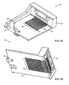
- FIG. 4A is a diagrammatic perspective top view of the electronic device module socket of FIG. 3.
- FIG. 4B is a diagrammatic perspective bottom view of the electronic device module socket of FIG. 3.
- FIG. 5A is a diagrammatic perspective side view of the flexible circuit based electronic device module of FIG. 3 without a top housing portion.
- FIG. 5B is a diagrammatic perspective bottom view of the flexible circuit based electronic device module of FIG. 5A, and an electrical connector of the socket of FIG. 3 coupled to a contact portion of the electronic device module.
- In the following description, like reference numbers are used to identify like elements. Furthermore, the drawings are intended to illustrate major features of exemplary embodiments in a diagrammatic manner. The drawings are not intended to depict every feature of actual embodiments nor relative dimensions of the depicted elements, and are not drawn to scale.
- Referring to FIGS. 1, 2A, 2B, 2C and 2D, in one embodiment, a socket-based electrical and mechanical
circuit connection system 10 includes asocket 12 and a socketable flexible circuit basedelectronic device module 14. -
Socket 12 is constructed and arranged to electrically and mechanically connectelectronic device module 14 to an interconnect substrate (e.g., a printed circuit board). In particular,socket 12 includes asupport frame 16, a pair ofretainers electrical connectors Support frame 16 has four sidewalls that define a recess for receivingelectronic device module 14. Eachretainer respective latch portion electronic device module 14 intosocket 12 and to snap back over a respective edge ofelectronic device module 14 whenelectronic device module 14 is fully seated withinsocket 12. In this way,retainers electronic device module 14 in place with respect tosocket 12. In some embodiments,support frame 16 andretainers support frame 16 andretainers -
Electrical connectors electrical conductors 29, each of which includes aspring finger portion 31 that protrudes into the recess defined by the sidewalls ofsupport frame 16. Eachspring finger portion 31 is biased (or spring loaded) against a corresponding electrical conductor of a contact portion of electronic device module 14 (described in detail below) when the electronic device module is held in place byretainers spring finger 29 preferably contacts the corresponding electrical conductor ofelectronic device module 14 over a relatively small area so that the contact pressure exerted by the spring fingers is relatively high. As shown in FIG. 2D, in this embodiment, eachspring finger portion 31 forms an "S"-shaped curve with the distal end extending away from the recess defined by the socket sidewalls. In other embodiments, each spring finger portion may form a "C"-shaped curve with the distal end extending toward the recess defined by the socket sidewalls. Still other spring finger arrangements are possible. -
Socket 12 may be connected to an interconnect substrate by any conventional surface mount process (e.g., an infrared solder reflow process). -
Electronic device module 14 includes ahousing 30, one or moreelectronic components 32 and aflexible circuit board 34. -
Housing 30 includes atop housing portion 36 that has a pair oftabs 38, 40 (FIG. 1) that are configured to engage a pair of mating latches 42, 44 of abottom housing portion 46.Top housing portion 36 also includes a pair of slots (not shown) that are configured to receive a pair offlanges bottom housing portion 46.Top housing portion 36 andbottom housing portion 46 each may be formed from a plastic material that is molded by a conventional injection molding process. In operation,flanges top housing portion 36 and latches 42, 44 snap down overtabs top housing portion 36 andbottom housing portion 46 together. - The
electronic components 32 may be semiconductor-based devices (e.g., integrated circuits and sensors) and other active or passive devices. In the illustrated embodiment,electronic components 32 correspond to the components of an image sensor (e.g., a CMOS image sensor available from Agilent Technologies, Inc. of Palo Alto, California, USA), including an image sensor chip and a number of peripheral electrical devices. -
Electronic components 32 are coupled mechanically and electrically byflexible circuit board 34.Flexible circuit board 34 may include a pattern of elongated electrical conductors formed on a plastic (e.g., polyimide) substrate surface. The electrical conductors may be formed from any one of a wide variety of electrically conductive materials, such as the electrically conductive materials that are used commonly in the circuit board industry. In one embodiment, the electrical conductors are formed from copper with nickel and gold plating.Electronic components 32 may be connected to the electrical conductor pattern offlexible circuit board 34 by a conventional wire bonding process. In the embodiments of FIGS. 1-2D,flexible circuit board 34 includes acomponent portion 52, a pair ofcontact portions curved portions couple contact portions component portion 52.Component portion 52 is substantially planar and corresponds to the area whereelectronic components 32 are mounted toflexible circuit board 34. Contactportions electronic components 32 by a plurality of electrical conductors that extend from thecontact portions curved portions component portion 52. In this embodiment,contact portions component portion 52 and extend outside of housing 30 (as shown in FIGS. 1 and 2D) to enableelectronic component module 14 to electrically couple to theelectrical connectors socket 12. To this end, the electrical conductors ofcontact portions flexible circuit board 34 that is opposite the surface on whichelectronic components 32 are mounted. The backsides ofcontact portions top housing portion 36 to resist the contact force exerted by the socketspring finger portions 31 whenelectronic device module 14 is fully seated withinsocket 12. - Referring to FIGS. 3, 4A, 4B, 5A and 5B, in another embodiment, a socket-based electrical and mechanical
circuit connection system 70 includes asocket 72 and a socketable flexible circuit basedelectronic device module 74. In this embodiment,socket 72 is configured to electrically connect to a contact portion of a flexible circuit board that is disposed at the bottom side ofelectronic device module 74. - As shown in FIGS. 4A and 4B,
socket 72 is constructed and arranged to electrically and mechanically connectelectronic device module 74 to an interconnect substrate (e.g., a printed circuit board). In particular,socket 72 includes asupport frame 76, aretainer 78, and anelectrical connector 82.Support frame 76 has two adjacent sidewalls that, together withretainer 78, define a recess for receivingelectronic device module 74.Retainer 78 includes alatch portion 86 that is configured to yield during insertion ofelectronic device module 74 intosocket 72 and to snap back over a respective edge ofelectronic device module 74 whenelectronic device module 74 is fully seated withinsocket 72. In this way,retainer 78 operates to mechanically holdelectronic device module 74 in place with respect tosocket 72. In some embodiments,support frame 76 andretainer 78 may be incorporated into a unitary structure, which may be formed from a plastic material that is molded by a conventional injection molding process. In other embodiments,support frame 76 andretainer 78 may be formed as separate components from any of a wide variety of different materials.Electrical connector 82 includes a plurality of resilientelectrical conductors 89, each of which includes aspring finger portion 91 that protrudes into the recess defined by the sidewalls ofsupport frame 76. Eachspring finger portion 91 is biased (or spring loaded) against a corresponding electrical conductor of a contact portion of electronic device module 74 (described in detail below) when theelectronic device module 74 is held in place byretainer 78. Eachspring finger 89 preferably contacts the corresponding electrical conductor ofelectronic device module 74 over a relatively small area so that the contact pressure exerted by the spring fingers is relatively high.Socket 72 may be connected to an interconnect substrate by any conventional surface mount process (e.g., an infrared solder reflow process). - Referring to FIGS. 3, 5A and 5B,
electronic device module 74 includes ahousing 90, one or moreelectronic components 92 and aflexible circuit board 94. -
Housing 90 may include a top portion and a bottom portion that may be constructed and arranged in a way that is similar to the construction and arrangement of electronic module housing 30 (described above).Housing 90 may be formed from a plastic material that is molded by a conventional injection molding process. - The
electronic components 92 may be semiconductor-based devices (e.g., integrated circuits and sensors) and other active or passive devices. In the illustrated embodiment,electronic components 92 correspond to the components of an image sensor (e.g., a CMOS image sensor available from Agilent Technologies, Inc. of Palo Alto, California, USA), including an image sensor chip and a number of peripheral electrical devices. -
Electronic components 92 are coupled mechanically and electrically byflexible circuit board 94.Flexible circuit board 94 may include a pattern of elongated electrical conductors formed on a plastic (e.g., polyimide) substrate surface. The electrical conductors may be formed from any one of a wide variety of electrically conductive materials that are used conventionally in the circuit board industry. In one embodiment, the electrical conductors are formed from copper with nickel and gold plating.Electronic components 92 may be connected to the electrical conductor pattern offlexible circuit board 94 by a conventional wire bonding process. In the embodiments of FIGS. 3-5B,flexible circuit board 94 includes acomponent portion 112, acontact portion 114, and acurved portion 118 that physicallycouple contact portion 114 tocomponent portion 112.Component portion 112 is substantially planar and corresponds to the area whereelectronic components 92 are mounted toflexible circuit board 94.Contact portion 114 is electrically coupled to theelectronic components 92 by a plurality of electrical conductors that extend from thecontact portion 114, throughcurved portion 118, to the pattern of electrical conductors formed incomponent portion 112. In this embodiment,contact portion 114 is oriented substantially parallel tocomponent portion 112 and extends outside ofhousing 90 to enableelectronic component module 74 to electrically couple to theelectrical connector 82 ofsocket 72. To this end,flexible circuit board 94 is folded atcurved portion 118, and the electrical conductors ofcontact portion 114 andelectronic components 92 are disposed on the same surface offlexible circuit board 94. The backside ofcontact portion 114 is supported byhousing 90 to resist the contact force exerted by the socketspring finger portions 91 whenelectronic device module 74 is fully seated withinsocket 72. - In sum, the above-described socket-based electrical and mechanical circuit connection systems provide unique ways in which electronic device modules may be positioned accurately and securely on an interconnect carrier, while allowing the electronic device modules to be replaced easily without having to desolder the modules and resolder new modules in their place.
- Other embodiments are within the scope of the claims.
- For example, in some embodiments, the spring loaded electrical conductors of the socket electrical connectors may be replaced by a conventional anisotropic electrically conductive film. In these embodiments, the retaining force applied by the socket retainers would be sufficient to hold the anisotropic electrically conductive film in electrical contact with the contact portions of the electronic device modules.
Claims (10)
- An electronic device module socket (12, 72) for electrically and mechanically connecting an interconnect substrate and an electronic device module (14, 74) having one or more electronic components (32, 92) mounted on a flexible circuit board (34, 94) supporting a plurality of elongated electrical conductors, the socket (12, 72) comprising:a support frame (16, 76) constructed and arranged to receive the electronic device module (14, 74);a retainer (18, 20, 78) constructed and arranged to engage and thereby mechanically hold the electronic device module (14, 74) in place; andan electrical connector (22, 82) constructed and arranged to electrically connect the plurality of elongated flexible circuit board conductors to a corresponding plurality of electrical conductors of the interconnect substrate.
- The electronic device module socket of claim 1, wherein the electrical connector (22, 82) is constructed and arranged to be biased against the plurality of elongated flexible circuit board conductors when the electronic device module (14, 74) is mechanically held in place by the retainer (18, 20, 78).
- The electronic device module socket of claim 2, wherein the electrical connector (22, 82) comprises a plurality of electrically conductive spring fingers.
- The electronic device module socket of claim 2, wherein the electrical connector (22, 82) comprises an elastomeric anisotropic electrically conductive film.
- The electronic device module socket of claim 1, wherein the retainer (18, 20, 78) has a latch portion configured to yield during insertion of the electronic device module (14, 74) into the socket (12, 72) and to snap back over an edge of the electronic device module (14, 74) when fully inserted into the socket (12, 72).
- A socketable electronic device module (14, 74), comprising:a housing (30, 90) constructed and arranged to be inserted within an electronic device module socket (12, 72) for electrical and mechanical connection to an interconnect substrate;one or more electronic components (32, 92); anda flexible circuit board (34, 94) comprising a flexible substrate having a component portion (52, 112) supporting the one or more electronic components (32, 92) and a contact portion (54, 56, 114) supporting a plurality of elongated electrical conductors and coupled to the component portion (52, 112) through a curved portion (58, 118), wherein the component portion (52, 112) of the flexible substrate is disposed within the housing (30, 90) and the contact portion (54, 56, 114) of the flexible substrate is disposed outside of the housing (30, 90) and is exposed for electrical contact with an electrical connector of the electronic device module socket (12, 72).
- The electronic device module of claim 6, wherein the one or more electronic components (32) are supported on one surface of the flexible substrate and at least a portion of the electrical conductors are supported on an opposite surface of the flexible substrate.
- The electronic device module of claim 7, wherein the contact portion (54, 56) of the flexible substrate is substantially orthogonal to the component portion (52) of the flexible substrate.
- The electronic device module of claim 6, wherein the one or more electronic components (92) and the electrical conductors are supported on the same surface of the flexible substrate.
- The electronic device module of claim 9, wherein the contact portion (114) of the flexible substrate is substantially parallel to the component portion (112) of the flexible substrate.
Applications Claiming Priority (2)
| Application Number | Priority Date | Filing Date | Title |
|---|---|---|---|
| US09/919,562 US6435882B1 (en) | 2001-07-27 | 2001-07-27 | Socketable flexible circuit based electronic device module and a socket for the same |
| US919562 | 2001-07-27 |
Publications (3)
| Publication Number | Publication Date |
|---|---|
| EP1280240A2 true EP1280240A2 (en) | 2003-01-29 |
| EP1280240A3 EP1280240A3 (en) | 2005-12-28 |
| EP1280240B1 EP1280240B1 (en) | 2011-09-14 |
Family
ID=25442314
Family Applications (1)
| Application Number | Title | Priority Date | Filing Date |
|---|---|---|---|
| EP02013011A Expired - Lifetime EP1280240B1 (en) | 2001-07-27 | 2002-06-12 | A socketable flexible circuit based electronic device module and a socket for the same |
Country Status (4)
| Country | Link |
|---|---|
| US (1) | US6435882B1 (en) |
| EP (1) | EP1280240B1 (en) |
| JP (1) | JP4210725B2 (en) |
| TW (1) | TW530437B (en) |
Families Citing this family (27)
| Publication number | Priority date | Publication date | Assignee | Title |
|---|---|---|---|---|
| JP3712982B2 (en) * | 2002-02-06 | 2005-11-02 | 株式会社ケーヒン | Electronic circuit board housing case |
| JP2004063391A (en) * | 2002-07-31 | 2004-02-26 | Mitsumi Electric Co Ltd | Module connector |
| GB0220751D0 (en) * | 2002-09-06 | 2002-10-16 | Nokia Corp | A camera connector |
| US6919623B2 (en) * | 2003-12-12 | 2005-07-19 | The Boeing Company | Hydrogen diffusion hybrid port and method of forming |
| JP2005310651A (en) * | 2004-04-23 | 2005-11-04 | Hirose Electric Co Ltd | Socket for electronic module |
| JP2005354545A (en) * | 2004-06-14 | 2005-12-22 | Agilent Technol Inc | Socket |
| US7918671B2 (en) * | 2004-07-13 | 2011-04-05 | Research In Motion Limited | Mounting structure with springs biasing towards a latching edge |
| JP4562538B2 (en) * | 2005-01-31 | 2010-10-13 | モレックス インコーポレイテド | Module socket |
| US7029308B2 (en) | 2005-02-17 | 2006-04-18 | Hirose Electric Co., Ltd. | Socket for electronic module |
| US20060189216A1 (en) * | 2005-02-18 | 2006-08-24 | Ming-Hsun Yang | Camera module connector keying structure |
| TWM271287U (en) * | 2005-02-18 | 2005-07-21 | Molex Taiwan Ltd | Camera module connector |
| JP4541226B2 (en) * | 2005-05-12 | 2010-09-08 | 富士通株式会社 | Module test method |
| JP4188942B2 (en) * | 2005-05-12 | 2008-12-03 | 日本航空電子工業株式会社 | connector |
| JP4464878B2 (en) * | 2005-07-11 | 2010-05-19 | 矢崎総業株式会社 | Electrical junction box |
| CN100377434C (en) * | 2005-08-05 | 2008-03-26 | 富士康(昆山)电脑接插件有限公司 | Electrical Connector Assembly |
| JP2009517160A (en) * | 2005-11-30 | 2009-04-30 | コーニンクレッカ フィリップス エレクトロニクス エヌ ヴィ | Electromechanical connector for thin medical monitoring patch |
| TWM304793U (en) * | 2006-04-03 | 2007-01-11 | Hon Hai Prec Ind Co Ltd | Electrical connector assembly |
| JP4699275B2 (en) * | 2006-04-27 | 2011-06-08 | 京セラ株式会社 | Electronics |
| TWM310502U (en) * | 2006-11-17 | 2007-04-21 | Molex Taiwan Ltd | Electrical connection device |
| DE102008000889B4 (en) * | 2008-03-31 | 2022-10-27 | Robert Bosch Gmbh | Removeable sensor and method for producing a removeable sensor by means of insertion and a non-positive/positive connection |
| JP5221255B2 (en) * | 2008-08-29 | 2013-06-26 | 矢崎総業株式会社 | Electrical junction box |
| JP5272636B2 (en) * | 2008-10-10 | 2013-08-28 | ミツミ電機株式会社 | Module connector |
| CN102074864B (en) * | 2009-11-20 | 2013-01-16 | 群康科技(深圳)有限公司 | Socket and socket assembly |
| US20120126678A1 (en) * | 2010-11-22 | 2012-05-24 | Nokia Corporation | Apparatus for Retaining an Object |
| US9106027B2 (en) * | 2012-12-21 | 2015-08-11 | Avago Technologies General Ip (Singapore) Pte. Ltd. | Methods, apparatuses and systems for mid-plane mounting parallel optical communications modules on circuit boards |
| JP6258898B2 (en) * | 2015-07-09 | 2018-01-10 | 矢崎総業株式会社 | Holding member and resin member manufacturing apparatus |
| US11432424B2 (en) * | 2021-01-15 | 2022-08-30 | Red Lion Controls, Inc. | Two piece panel latch and method |
Family Cites Families (14)
| Publication number | Priority date | Publication date | Assignee | Title |
|---|---|---|---|---|
| US4489999A (en) | 1983-02-15 | 1984-12-25 | Motorola, Inc. | Socket and flexible PC board assembly and method for making |
| US4699593A (en) * | 1986-01-14 | 1987-10-13 | Amp Incorporated | Connector having contact modules for a substrate such as an IC chip carrier |
| US4832612A (en) * | 1986-10-31 | 1989-05-23 | Amp Incorporated | Protective carrier and securing means therefor |
| US5072284A (en) | 1988-11-25 | 1991-12-10 | Fuji Photo Film Co., Ltd. | Solid state image pickup device |
| US5485351A (en) | 1989-06-09 | 1996-01-16 | Labinal Components And Systems, Inc. | Socket assembly for integrated circuit chip package |
| US4954878A (en) * | 1989-06-29 | 1990-09-04 | Digital Equipment Corp. | Method of packaging and powering integrated circuit chips and the chip assembly formed thereby |
| US5026297A (en) * | 1990-06-28 | 1991-06-25 | Molex Incorporated | Electrical socket assembly for single in-line circuit package |
| JPH05206427A (en) | 1992-01-09 | 1993-08-13 | Nec Corp | Solid-state imaging device |
| US5199882A (en) * | 1992-03-19 | 1993-04-06 | Amp Incorporated | Elastomeric wire to pad connector |
| US5785535A (en) | 1996-01-17 | 1998-07-28 | International Business Machines Corporation | Computer system with surface mount socket |
| US6011294A (en) | 1996-04-08 | 2000-01-04 | Eastman Kodak Company | Low cost CCD packaging |
| JP3677756B2 (en) | 1996-08-30 | 2005-08-03 | コニカミノルタフォトイメージング株式会社 | Card connector and electronic device equipped with the same |
| JP3694165B2 (en) * | 1998-02-25 | 2005-09-14 | 株式会社エンプラス | IC socket |
| JP3343071B2 (en) | 1998-03-03 | 2002-11-11 | 富士写真フイルム株式会社 | Image sensor mounting method |
-
2001
- 2001-07-27 US US09/919,562 patent/US6435882B1/en not_active Expired - Lifetime
-
2002
- 2002-02-26 TW TW091103451A patent/TW530437B/en not_active IP Right Cessation
- 2002-06-12 EP EP02013011A patent/EP1280240B1/en not_active Expired - Lifetime
- 2002-07-29 JP JP2002219387A patent/JP4210725B2/en not_active Expired - Fee Related
Also Published As
| Publication number | Publication date |
|---|---|
| EP1280240A3 (en) | 2005-12-28 |
| JP2003133021A (en) | 2003-05-09 |
| EP1280240B1 (en) | 2011-09-14 |
| JP4210725B2 (en) | 2009-01-21 |
| US6435882B1 (en) | 2002-08-20 |
| TW530437B (en) | 2003-05-01 |
Similar Documents
| Publication | Publication Date | Title |
|---|---|---|
| US6435882B1 (en) | Socketable flexible circuit based electronic device module and a socket for the same | |
| US5953214A (en) | Dual substrate package assembly coupled to a conducting member | |
| US6721189B1 (en) | Memory module | |
| US6358064B2 (en) | Z-axis electrical interconnect | |
| US20090023330A1 (en) | Systems For Electrically Connecting Processing Devices Such As Central Processing Units And Chipsets | |
| US6804119B2 (en) | Method and edge connector providing electrostatic discharge arrest features and digital camera employing same | |
| EP0920090A2 (en) | Printed circuit connector | |
| US5035629A (en) | Electrical connector | |
| US5967831A (en) | Electrical connector assembly | |
| US20060244111A1 (en) | Electrical connecting member capable of achieving stable connection with a simple structure and connector using the same | |
| US11503732B1 (en) | Socket alignment and retention system | |
| US12424785B2 (en) | Receptacle connector | |
| US20020016094A1 (en) | Mounting electronic components on circuit boards | |
| CN116365270A (en) | Socket connector | |
| KR20080007625A (en) | Connector assembly | |
| US20100203747A1 (en) | Flexible printed circuit board having embossed contact engaging portion | |
| US4629267A (en) | Circuit terminating device | |
| EP1209764A1 (en) | Strain relief for BGA connector | |
| US20050176288A1 (en) | Module connector | |
| US20250125548A1 (en) | Receptacle connector | |
| JPH08512168A (en) | High-density electronic device connector | |
| US4702706A (en) | Electrical connecting device including socket therefor | |
| EP0871992B1 (en) | Electrical connector assembly | |
| US4580857A (en) | Circuit terminating clip | |
| US4575165A (en) | Circuit to post interconnection device |
Legal Events
| Date | Code | Title | Description |
|---|---|---|---|
| PUAI | Public reference made under article 153(3) epc to a published international application that has entered the european phase |
Free format text: ORIGINAL CODE: 0009012 |
|
| AK | Designated contracting states |
Designated state(s): AT BE CH CY DE DK ES FI FR GB GR IE IT LI LU MC NL PT SE TR |
|
| AX | Request for extension of the european patent |
Extension state: AL LT LV MK RO SI |
|
| PUAL | Search report despatched |
Free format text: ORIGINAL CODE: 0009013 |
|
| AK | Designated contracting states |
Kind code of ref document: A3 Designated state(s): AT BE CH CY DE DK ES FI FR GB GR IE IT LI LU MC NL PT SE TR |
|
| AX | Request for extension of the european patent |
Extension state: AL LT LV MK RO SI |
|
| 17P | Request for examination filed |
Effective date: 20060626 |
|
| AKX | Designation fees paid |
Designated state(s): DE FI GB SE |
|
| 17Q | First examination report despatched |
Effective date: 20061010 |
|
| RAP1 | Party data changed (applicant data changed or rights of an application transferred) |
Owner name: AGILENT TECHNOLOGIES, INC. |
|
| RAP1 | Party data changed (applicant data changed or rights of an application transferred) |
Owner name: MICRON TECHNOLOGY, INC. |
|
| RAP1 | Party data changed (applicant data changed or rights of an application transferred) |
Owner name: APTINA IMAGING CORPORATION |
|
| REG | Reference to a national code |
Ref country code: DE Ref legal event code: R079 Ref document number: 60241005 Country of ref document: DE Free format text: PREVIOUS MAIN CLASS: H01R0012240000 Ipc: H01R0012000000 |
|
| GRAP | Despatch of communication of intention to grant a patent |
Free format text: ORIGINAL CODE: EPIDOSNIGR1 |
|
| RIC1 | Information provided on ipc code assigned before grant |
Ipc: H01R 12/00 20060101AFI20110224BHEP |
|
| GRAS | Grant fee paid |
Free format text: ORIGINAL CODE: EPIDOSNIGR3 |
|
| GRAA | (expected) grant |
Free format text: ORIGINAL CODE: 0009210 |
|
| AK | Designated contracting states |
Kind code of ref document: B1 Designated state(s): DE FI GB SE |
|
| REG | Reference to a national code |
Ref country code: GB Ref legal event code: FG4D |
|
| REG | Reference to a national code |
Ref country code: DE Ref legal event code: R096 Ref document number: 60241005 Country of ref document: DE Effective date: 20111110 |
|
| PG25 | Lapsed in a contracting state [announced via postgrant information from national office to epo] |
Ref country code: FI Free format text: LAPSE BECAUSE OF FAILURE TO SUBMIT A TRANSLATION OF THE DESCRIPTION OR TO PAY THE FEE WITHIN THE PRESCRIBED TIME-LIMIT Effective date: 20110914 Ref country code: SE Free format text: LAPSE BECAUSE OF FAILURE TO SUBMIT A TRANSLATION OF THE DESCRIPTION OR TO PAY THE FEE WITHIN THE PRESCRIBED TIME-LIMIT Effective date: 20110914 |
|
| PLBE | No opposition filed within time limit |
Free format text: ORIGINAL CODE: 0009261 |
|
| STAA | Information on the status of an ep patent application or granted ep patent |
Free format text: STATUS: NO OPPOSITION FILED WITHIN TIME LIMIT |
|
| 26N | No opposition filed |
Effective date: 20120615 |
|
| REG | Reference to a national code |
Ref country code: DE Ref legal event code: R097 Ref document number: 60241005 Country of ref document: DE Effective date: 20120615 |
|
| GBPC | Gb: european patent ceased through non-payment of renewal fee |
Effective date: 20120612 |
|
| REG | Reference to a national code |
Ref country code: GB Ref legal event code: S28 Free format text: APPLICATION FILED |
|
| REG | Reference to a national code |
Ref country code: GB Ref legal event code: S28 Free format text: RESTORATION ALLOWED Effective date: 20140129 |
|
| PGFP | Annual fee paid to national office [announced via postgrant information from national office to epo] |
Ref country code: GB Payment date: 20150526 Year of fee payment: 14 |
|
| PGFP | Annual fee paid to national office [announced via postgrant information from national office to epo] |
Ref country code: DE Payment date: 20150630 Year of fee payment: 14 |
|
| PG25 | Lapsed in a contracting state [announced via postgrant information from national office to epo] |
Ref country code: GB Free format text: THE PATENT HAS BEEN ANNULLED BY A DECISION OF A NATIONAL AUTHORITY Effective date: 20120612 |
|
| REG | Reference to a national code |
Ref country code: DE Ref legal event code: R119 Ref document number: 60241005 Country of ref document: DE |
|
| GBPC | Gb: european patent ceased through non-payment of renewal fee |
Effective date: 20160612 |
|
| PG25 | Lapsed in a contracting state [announced via postgrant information from national office to epo] |
Ref country code: DE Free format text: LAPSE BECAUSE OF NON-PAYMENT OF DUE FEES Effective date: 20170103 |
|
| PG25 | Lapsed in a contracting state [announced via postgrant information from national office to epo] |
Ref country code: GB Free format text: THE PATENT HAS BEEN ANNULLED BY A DECISION OF A NATIONAL AUTHORITY Effective date: 20160612 |