EP1280233A1 - Antenna element and portable communication terminal - Google Patents
Antenna element and portable communication terminal Download PDFInfo
- Publication number
- EP1280233A1 EP1280233A1 EP00915521A EP00915521A EP1280233A1 EP 1280233 A1 EP1280233 A1 EP 1280233A1 EP 00915521 A EP00915521 A EP 00915521A EP 00915521 A EP00915521 A EP 00915521A EP 1280233 A1 EP1280233 A1 EP 1280233A1
- Authority
- EP
- European Patent Office
- Prior art keywords
- antenna
- antenna element
- present
- plate
- monopole
- Prior art date
- Legal status (The legal status is an assumption and is not a legal conclusion. Google has not performed a legal analysis and makes no representation as to the accuracy of the status listed.)
- Withdrawn
Links
Images









Classifications
-
- H—ELECTRICITY
- H01—ELECTRIC ELEMENTS
- H01Q—ANTENNAS, i.e. RADIO AERIALS
- H01Q21/00—Antenna arrays or systems
- H01Q21/30—Combinations of separate antenna units operating in different wavebands and connected to a common feeder system
-
- H—ELECTRICITY
- H01—ELECTRIC ELEMENTS
- H01Q—ANTENNAS, i.e. RADIO AERIALS
- H01Q1/00—Details of, or arrangements associated with, antennas
- H01Q1/12—Supports; Mounting means
- H01Q1/22—Supports; Mounting means by structural association with other equipment or articles
- H01Q1/24—Supports; Mounting means by structural association with other equipment or articles with receiving set
- H01Q1/241—Supports; Mounting means by structural association with other equipment or articles with receiving set used in mobile communications, e.g. GSM
- H01Q1/242—Supports; Mounting means by structural association with other equipment or articles with receiving set used in mobile communications, e.g. GSM specially adapted for hand-held use
-
- H—ELECTRICITY
- H01—ELECTRIC ELEMENTS
- H01Q—ANTENNAS, i.e. RADIO AERIALS
- H01Q1/00—Details of, or arrangements associated with, antennas
- H01Q1/12—Supports; Mounting means
- H01Q1/22—Supports; Mounting means by structural association with other equipment or articles
- H01Q1/24—Supports; Mounting means by structural association with other equipment or articles with receiving set
- H01Q1/241—Supports; Mounting means by structural association with other equipment or articles with receiving set used in mobile communications, e.g. GSM
- H01Q1/242—Supports; Mounting means by structural association with other equipment or articles with receiving set used in mobile communications, e.g. GSM specially adapted for hand-held use
- H01Q1/243—Supports; Mounting means by structural association with other equipment or articles with receiving set used in mobile communications, e.g. GSM specially adapted for hand-held use with built-in antennas
-
- H—ELECTRICITY
- H01—ELECTRIC ELEMENTS
- H01Q—ANTENNAS, i.e. RADIO AERIALS
- H01Q1/00—Details of, or arrangements associated with, antennas
- H01Q1/12—Supports; Mounting means
- H01Q1/22—Supports; Mounting means by structural association with other equipment or articles
- H01Q1/24—Supports; Mounting means by structural association with other equipment or articles with receiving set
- H01Q1/241—Supports; Mounting means by structural association with other equipment or articles with receiving set used in mobile communications, e.g. GSM
- H01Q1/242—Supports; Mounting means by structural association with other equipment or articles with receiving set used in mobile communications, e.g. GSM specially adapted for hand-held use
- H01Q1/243—Supports; Mounting means by structural association with other equipment or articles with receiving set used in mobile communications, e.g. GSM specially adapted for hand-held use with built-in antennas
- H01Q1/244—Supports; Mounting means by structural association with other equipment or articles with receiving set used in mobile communications, e.g. GSM specially adapted for hand-held use with built-in antennas extendable from a housing along a given path
-
- H—ELECTRICITY
- H01—ELECTRIC ELEMENTS
- H01Q—ANTENNAS, i.e. RADIO AERIALS
- H01Q1/00—Details of, or arrangements associated with, antennas
- H01Q1/36—Structural form of radiating elements, e.g. cone, spiral, umbrella; Particular materials used therewith
-
- H—ELECTRICITY
- H01—ELECTRIC ELEMENTS
- H01Q—ANTENNAS, i.e. RADIO AERIALS
- H01Q21/00—Antenna arrays or systems
- H01Q21/28—Combinations of substantially independent non-interacting antenna units or systems
Definitions
- This present invention relates to an antenna element and a portable information terminal, particularly to an antenna element used in a portable telephone and a portable telephone using the antenna.
- a monopole antenna or a helical antenna set up to extend in the longitudinal direction of their case As an antenna element for transmission and reception in portable telephones, there has been hitherto known, for example, a monopole antenna or a helical antenna set up to extend in the longitudinal direction of their case.
- the impedance of such an antenna element is different from the impedance of a radio section inside the portable telephones. It is therefore necessary to match these impedances with each other.
- a matching circuit is arranged between their radio section and their antenna element.
- a portable information terminal which can achieve two functions as a portable telephone and a personal handy-phone system (PHS) has been developed.
- a portable telephone and a PHS are different from each other in the radio frequencies (band) used for transmission and reception of information.
- an antenna is generally designed in the manner that the voltage standing wave ratio (VSWR) of the antenna is set to 2 or less in the band. It is therefore necessary that in the portable information terminal which can achieve two functions as a portable telephone and a PHS, the VSWR of its antenna is set to 2 or less in plural bands or a broad band.
- the band in which the VSWR of the antennas is 2 or less is narrow. Thus, it is difficult that the conventional antennas are used as portable information terminals having the above-mentioned plural functions.
- the conventional matching circuit is composed of lumped-parameter elements such as a coil and a condenser. Therefore, when electrical signals are transmitted from a radio section to an antenna element through the matching circuit, loss is generated in the coil and condenser in the matching circuit to cause a problem that transmission efficiency of the electrical signals is lowered.
- the present invention has been made to overcome the above-mentioned problems.
- An object of the present invention is to provide an antenna element and a portable information terminal in which loss of electrical signals is small to give high efficiency.
- Another object of the present invention is to provide an antenna element and a portable information terminal having a broad usable band.
- the antenna element according to the present invention includes a first antenna part which is substantially equivalent to a series resonant circuit, and a second antenna part which is brought with contact with and connected to the first antenna part and is substantially equivalent to a parallel resonant circuit.
- the first antenna part is substantially equivalent to the series resonant circuit and the second antenna part is substantially equivalent to the parallel resonant circuit. Therefore, the first antenna part and the second antenna part have impedance characteristics reverse to each other. By jointing the two antenna parts having the reverse impedance characteristics in above-mentioned way, their reactances are mutually cancelled out. In this way, the impedance of the antenna element and that of a radio section can be matched with each other so that a usable band can be made broad without using any matching circuit.
- the antenna element of the present invention has a high efficiency.
- the first antenna part and the second antenna part are fitted in series to a feeding point.
- the first antenna part and the second antenna part are fitted in parallel to a feeding point.
- the first antenna part includes a plate antenna
- the second antenna part includes a linear antenna
- the linear antenna includes at least one selected from the group consisting of a monopole antenna and a helical antenna.
- the antenna element further includes a substrate whose surface has an electrical conductivity; the first antenna part is set up, through a dielectric, over the surface of the substrate; and the second antenna part is set up to extend from the substrate.
- the first antenna part is set up, through the dielectric, over the surface of the substrate; therefore, the wavelength of a radio wave advancing in the first antenna part can be made short.
- the length of the first antenna part can be made short so that the size of the antenna element can be made small.
- the second antenna part is set up to extend from the substrate; therefore, the second antenna part can transmit and receive the radio wave certainly without being affected by the substrate.
- the antenna element further includes a substrate whose surface has an electrical conductivity; and the first antenna part and the second antenna part are set up, through a dielectric, over the surface of the substrate.
- the first antenna part and the second antenna part are set up, through the dielectric, over the surface of the substrate; therefore, the wavelength of a radio wave advancing in the first and second antenna parts can be made short.
- the size of the first and second antenna parts can be made small so that the size of the antenna element can be made small.
- the second antenna part includes at least one selected from the group consisting of a monopole antenna, a helical antenna, a meander line antenna, and a zigzag antenna.
- the portable information terminal includes an antenna element including a first antenna part which is substantially equivalent to a series resonant circuit, and a second antenna part which is brought with contact with and connected to the first antenna part and is substantially equivalent to a parallel resonant circuit.
- the first antenna part is substantially equivalent to the series resonant circuit and the second antenna part is substantially equivalent to the parallel resonant circuit. Therefore, the first antenna part and the second antenna part have impedance characteristics reverse to each other. By jointing the two antenna parts having the reverse impedance characteristics, their reactances are mutually cancelled out. Thus, the impedance of the antenna element and that of a radio section can be matched with each other. As a result, the portable information terminal has a broad usable band.
- the portable information terminal of the present invention has a high efficiency.
- Fig. 1 is a plan view of an antenna element according to the first embodiment of the present invention.
- an antenna element 1a has a plate antenna 13 as a first antenna part which is substantially equivalent to a series resonant circuit, a monopole antenna 14a as a second antenna part which is connected to plate antenna 13 and is substantially equivalent to a parallel resonant circuit, and a metal substrate 11 as a base plate.
- Plate antenna 13 is composed of a microstrip line. The electric length of plate antenna 13 is about ⁇ /4.
- a feeding point 12 is connected to one end of plate antenna 13.
- Feeding point 12 is a point which is connected to a given radio section. The radio section and plate antenna 13 are connected to each other through feeding point 12.
- Monopole antenna 14a is connected to the other end of plate antenna 13.
- Monopole antenna 14a is formed to extend in the longitudinal direction of metal substrate 11. Monopole antenna 14a and plate antenna 13 are fitted in series to feeding point 12. The electric length of monopole antenna 14a is about 3 ⁇ /8. This monopole antenna 14a has the so-called anti-resonance characteristic. Monopole antenna 14a and plate antenna 13 fulfill functions for transmission and reception of radio waves.
- Metal substrate 11 is formed by depositing a metal layer (for example, a copper layer) on a given insulating substrate.
- the metal layer deposited on the insulating substrate has an electric conductivity which is substantially equal to that of copper.
- Metal substrate 11 is substantially rectangular. Long sides thereof are along the direction in which monopole antenna 14a extends.
- Fig. 2 is a side view of the antenna element, as is viewed from the direction shown by an arrow II in Fig. 1.
- antenna element 1a has metal substrate 11, plate antenna 13 and monopole antenna 14a.
- Metal substrate 11 is in the form of a thin plate and is formed so as to extend in one direction.
- the radio section (not illustrated) is fitted up onto metal substrate 11. This radio section is connected to plate antenna 13 through feeding point 12.
- Plate antenna 13 is in an L-shaped member. One end of plate antenna 13 is connected to feeding point 12. The other end thereof is connected to monopole antenna 14a.
- a dielectric 15 is inserted between plate antenna 13 and metal substrate 11.
- Dielectric 15 is made of Teflon (relative dielectric constant: 2.1).
- Plate antenna 13 is made of copper.
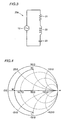
- Fig. 3 is an equivalent circuit diagram of the plate antenna.
- Fig. 4 is a Smith chart for explaining the property of the plate antenna.
- plate antenna 13 is substantially equivalent to a series resonant circuit 20a wherein a resistance 21, a coil 22 and a condenser 23 are connected in series to feeding point 12.
- the imaginary part of the impedance of the plate antenna is positive as shown at a point H since this antenna is substantially equivalent to the series resonant circuit as illustrated in Fig. 3.
- the imaginary part of the impedance is negative as shown at a point L .
- Fig. 5 is an equivalent circuit diagram of the monopole antenna.
- Fig. 6 is a Smith chart for explaining the property of the monopole antenna.
- the monopole antenna is substantially equivalent to a parallel resonant circuit 20b wherein a resistance 21, a coil 22 and a condenser 23 are connected in parallel to feeding point 12.
- the imaginary part of the impedance of monopole antenna 14a is negative.
- the imaginary part of the impedance is positive as shown at a point L .
- Fig. 7 is an equivalent circuit diagram of the antenna element illustrated in Figs. 1 and 2.
- antenna element 1a is equivalent to a circuit wherein series resonant circuit 20a and parallel resonant circuit 20b are jointed to each other.
- Fig. 8 is a Smith chart for explaining the property of the antenna illustrated in Figs. 1 and 2.
- the Smith chart of the antenna according to the present invention is a synthesis of the Smith chart of the plate antenna, shown in Fig. 4, and the Smith chart of the monopole antenna, shown in Fig. 6. That is, the imaginary part of the impedance is negative to the radio wave having the highest frequency, shown at a point H .
- the reflection coefficient (the distance from the center of the Smith chart to point H ) to the radio wave shown at point H in Fig. 8 is smaller than the reflection coefficient at point H in Figs. 4 and 6.
- the frequency becomes smaller, the track of the impedance is nearer to the central point.
- the imaginary part of the impedance is zero.
- the track of the impedance is shifted to be away from the central point.
- the track reaches a point L having the smallest frequency.
- the reflection coefficient at point L in Fig. 8 is smaller than that at points L shown in Figs. 4 and 6.
- the electric length of monopole antenna 14a can be made to an electric length represented by 3 ⁇ /8 + ( ⁇ /2) ⁇ N, wherein N is an integer, and having anti-resonance characteristic.
- the electric length of plate antenna 13 can be made to an electric length represented by ⁇ /4 + ( ⁇ /2) ⁇ N, wherein N is an integer, and having resonance characteristic.
- plate antenna 13 and monopole antenna 14a are set up over one surface of metal substrate 11, but plate antennas 13 and monopole antennas 14a may be set up over both surfaces of metal substrate 11.
- Fig. 9 is a plan view of an antenna element according to the second embodiment of the present invention.
- an antenna element 1b according to the second embodiment is different from antenna element 1a illustrated in Figs. 1 and 2 in that antenna element 1b has a helical antenna 14b as the second antenna part.
- Helical antenna 14b generally has a narrow usable band. According to the present invention, even if helical antenna 14b is used, an antenna element having a broad usable band can be produced.
- the physical length of the antenna element can be made small.
- Fig. 10 is a plan view of an antenna element according to the third embodiment of the present invention.
- an antenna element 1c according to the third embodiment is different from antenna element 1a illustrated in Figs. 1 and 2, wherein only monopole antenna 14a is set up as the first antenna part, in that a monopole antenna 14a and a helical antenna 14b are set up as the first antenna part.
- Antenna element 1c having the above-mentioned structure also has the same advantages as the antenna element illustrated in Fig. 1. Furthermore, by combining monopole antenna 14a with helical antenna 14b, properties dependently on use or purposes can be exhibited.
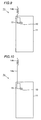
- Fig. 11 is a plan view of an antenna element according to the fourth embodiment of the present invention.
- an antenna element 1d according to the fourth embodiment is different from antenna element 1a illustrated in Figs. 1 and 2, wherein monopole antenna 14a is set up to extend from metal substrate 11, in that a meander line antenna 14d is used as the first antenna part and this meander line antenna 14d is set up on metal substrate 11.
- Meander line antenna 14d is set up to interpose air between antenna 14d and metal substrate 11. One end of antenna 14d is connected to a plate antenna 13.
- Antenna element 1d having the above-mentioned structure also has the same advantages as antenna element 1a illustrated in Figs. 1 and 2. Furthermore, an antenna, such as monopole antenna 14a illustrated in Figs. 1 and 2, does not project from metal substrate 11 since meander line antenna 14d is made on metal substrate 11. As a result, the whole of antenna element 1d can be made thin and small.
- Fig. 12 is a plan view of an antenna element according to the fifth embodiment of the present invention.
- an antenna element 1e according to the fifth embodiment is different from antenna element 1d illustrated in Fig. 11, which has meander line antenna 14d as the second antenna part, in that antenna element 1e has a helical antenna 14e as the second antenna part.
- Antenna element 1e having the above-mentioned structure also has the same advantages as antenna element 1d illustrated in Fig. 11.
- Fig. 13 is a plan view of an antenna element according to the sixth embodiment of the present invention.
- an antenna element 1f according to the sixth embodiment is different from antenna element 1d illustrated in Fig. 11, which has meander line antenna 14d as the second antenna part, in that antenna element if has a zigzag antenna 14f as the second antenna part.
- Antenna element 1f having the above-mentioned structure also has the same advantages as antenna element 1d illustrated in Fig. 11.
- Fig. 14 is a plan view of an antenna element according to the seventh embodiment of the present invention.
- an antenna element 1g according to the seventh embodiment is different from antenna element 1d illustrated in Fig. 11, which has meander line antenna 14d as the second antenna, in that antenna element 1g has a monopole antenna 14g as the second antenna.
- Antenna element 1g having the above-mentioned structure also has the same advantages as antenna element 1d illustrated in Fig. 11.
- Fig. 15 is a plan view of an antenna element according to the eighth embodiment of the present invention.
- an antenna element 1h according to the eighth embodiment is different from antenna element 1d illustrated in Fig. 11, which has no dielectric 18, in that a dielectric 18 is formed on a metal substrate 11 and a plate antenna 13 and a meander line antenna 14d are formed on dielectric 18.
- Dielectric 18 is made of a material having a small dielectric tangent tan ⁇ and a high relative dielectric constant, for example, a ceramic material(relative dielectric constant ⁇ 7-100), Teflon (relative dielectric constant ⁇ 2.1) or a resin material (relative dielectric constant ⁇ 3.3) such as Vectra.
- Antenna element 1h having the above-mentioned structure has the same advantages as antenna element 1d illustrated in Fig. 11. Since plate antenna 13 and meander line antenna 14d are put on dielectric 18 having a high relative dielectric constant, the wavelength of a radio wave advancing in plate antenna 13 and meander line antenna 14d can be made short. As a result, the size of plate antenna 13 and meander line antenna 14d can be made small. The size of metal substrate 11 can also be made small.
- Fig. 16 is a plan view of an antenna element according to the ninth embodiment of the present invention.
- an antenna element 1i according to the ninth embodiment is different from antenna element 1h illustrated in Fig. 15 in that antenna element 1i has a helical antenna 14e as the second antenna part.
- Antenna element 1i having the above-mentioned structure has the same advantages as antenna element 1h illustrated in Fig. 15.
- Fig. 17 is a plan view of an antenna element according to the tenth embodiment of the present invention.
- an antenna element 1j according to the tenth embodiment is different from antenna element 1h illustrated in Fig. 15 in that antenna element 1j has a zigzag antenna 14f as the second antenna part.
- Antenna element 1j having the above-mentioned structure has the same advantages as antenna element 1h illustrated in Fig. 15.
- Fig. 18 is a plan view of an antenna element according to the eleventh embodiment of the present invention.
- an antenna element 1k according to the eleventh embodiment is different from antenna element 1h illustrated in Fig. 15 in that antenna element 1k has a monopole antenna 14g as the second antenna.
- Antenna element 1k having the above-mentioned structure also has the same advantages as antenna element 1h illustrated in Fig. 15.
- Fig. 19 is a perspective view of an antenna element according to the twelfth embodiment of the present invention.
- an antenna element 1m according to the twelfth embodiment has a metal substrate 11, a plate member 19, a plate antenna 13, and a meander line antenna 14d.
- Plate member 19 is fixed to metal substrate 11.
- Plate member 19 has a structure wherein a dielectric and a metal plate overlap with each other. Plate member 19 is fitted perpendicularly to metal substrate 11. Therefore, metal substrate 11 and plate member 19 are jointed to each other to form an L-shaped base plate. Plate member 19 is set up on the top face of metal substrate 11.
- Plate antenna 13 and meander line antenna 14d are made on plate member 19. Plate antenna 13 is connected to a feeding point 12. Plate antenna 13 and meander line antenna 14d spread to extend in the direction perpendicular to the main face of metal substrate 11.
- Antenna element 1m having the above-mentioned structure has the same advantages as antenna element 1a illustrated in Figs. 1 and 2.
- the length of the longitudinal direction of metal substrate 11 can be made short since plate antenna 13 and meander line antenna 14d are put on plate member 19 set up perpendicularly to metal substrate 11. For this reason, the size of metal substrate 11 can be made small and the area for mounting the antenna element can be made small.
- Fig. 20 is a perspective view of an antenna element according to the thirteenth embodiment of the present invention and a portable telephone using this antenna element.
- a portable telephone 50a according to the present invention has an antenna element 1n and a rear case 32 for storing this antenna element.
- Antenna element 1n has a plate antenna 13 as a first antenna part, a monopole antenna 14a as a second antenna part, and a metal substrate 11 as a base plate.
- Plate antenna 13 and monopole antenna 14a are fixed to rear case 32.
- Plate antenna 13 is set in rear case 32, and monopole antenna 14a is set to project from rear case 32.
- Plate antenna 13 and monopole antenna 14a are connected to each other.
- a feeding point 12 is set on metal substrate 11. Feeding point 12 is connected to one end of plate antenna 13 through a metal pin 31.
- Metal substrate 11 is also stored in rear case 32.
- a non-illustrated radio section is made on metal substrate 11.
- Antenna element 1n having the above-mentioned structure has the same constitution as antenna element 1a illustrated in Figs. 1 and 2, so as to have the same advantages as antenna element 1a illustrated in Figs. 1 and 2.
- portable telephone 50a has a broad usable band since it has antenna element 1h.
- telephone 50a makes it possible to transmit and receive radio waves having broad frequencies.
- two functions of PHS and a portable telephone can be fulfilled.
- this antenna element Since this antenna element has no matching circuit, loss of electric signals by a matching circuit is not generated.
- Fig. 21 is a perspective view of an antenna element according to the fourteenth embodiment of the present invention and a portable telephone using this antenna element.
- a portable telephone 50b according to the present invention has an antenna element 1p and a rear case 32.
- Antenna element 1p is different from antenna element 1n illustrated in Fig. 20, which has no contact spring, in that antenna element 1p has a contact spring 34 which also functions as an antenna at one end of a plate antenna 13.
- Contact spring 34 is connected to a feeding point 12.
- Antenna element 1p having the above-mentioned structure has the same advantages as antenna element 1n illustrated in Fig. 20.
- portable telephone 50b using this antenna element 1p has a broad usable band and gives a small loss in the same way as portable telephone 50a illustrated in Fig. 20.
- Fig. 22 is a plan view of an antenna element according to the fifteenth embodiment of the present invention.
- an antenna element 1q has a monopole antenna 14a as a first antenna part, a plate antenna 13 as a second antenna part, and a metal substrate 11.
- Monopole antenna 14a is set up to extend from metal substrate 11.
- Monopole antenna 14a and plate antenna 13 are connected in parallel to a feeding point 12.
- monopole antenna 14a may be substituted with the above-mentioned helical antenna 14b or 14e, zigzag antenna 14f, meander line antenna 14d, monopole antenna 14g or the like.
- Monopole antenna 14a may be put on metal substrate 11.
- a material having a high dielectric constant may be interposed between monopole antenna 14a, plate antenna 13 and metal substrate 11.
- Fig. 23 is an equivalent circuit diagram of the antenna element illustrated in Fig. 22.
- plate antenna 13 is substantially equivalent to a series resonant circuit 20a wherein a resistance 21, a coil 22 and a condenser 23 are connected in series to each other.
- Monopole antenna 14a is substantially equivalent to a parallel resonant circuit 20b wherein a resistance 21, a coil 22 and a condenser 23 are connected in parallel to each other. The two circuits are jointed to each other.
- Fig. 24 is a Smith chart for explaining the impedance property of the antenna element illustrated in Fig. 22.
- the imaginary part of the impedance of antenna element 1q is positive as shown at a point H .
- the imaginary part of the impedance approaches zero.
- the track of the impedance moves to surround the central point of the Smith chart.
- the imaginary part of the impedance becomes negative.
- the imaginary part of the impedance is most negative so that the track is apart from the central point of the Smith chart.
- the Smith chart shown in Fig. 24 is compared with the Smith charts of the plate antenna and the monopole antenna shown in Figs. 4 and 6.
- the distance between points H & L and the center of the chart is shorter than the distance between points H & L of in the Smith chart shown in Figs. 4 and 6 and the center of this chart.
- series resonant circuit 20a and parallel resonant circuit 20b have different properties and the circuits are jointed to each other so that their properties are mutually cancelled out. In this manner, impedance-matching is attained.
- antenna element 1q has a small reflection coefficient over a broad band so that element 1q can be used in the broad band.
- Impedance-matching can be attained without using any matching circuit. Therefore, loss of electrical signals in a matching circuit, as is conventionally seen, is not generated.
- Fig. 25 is a circuit diagram of a conventional antenna element.
- the antenna element was composed of an antenna 114, a coil 122, a stub 124 and a condenser 123.
- Coil 122 has an inductance of 6.8 nH.
- Condenser 123 has a capacity of 4 pF.
- Antenna 114 is composed of a monopole antenna and has a length of 55 mm (electric length: 3 ⁇ /8).
- a radio wave having frequencies of 1.5 GHz to 2.5 GHz was inputted to the antenna element having the above-mentioned matching circuit, and then the impedance, the Smith chart and the VSWR of the antenna element were examined.
- Table 1 Point Frequency (GHz) Impedance of the antenna element having the matching circuit( ⁇ ) VSWR Real part( ⁇ ) Imaginary part( ⁇ ) 201 1.92 58 0 1.2 202 1.98 44 3 1.3 203 2.11 48 14 1.4 204 2.17 48 -10 1.4
- the smith chart is shown in Fig. 26.
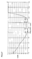
- a relationship between the frequency and the VSWR is shown in Fig. 27.
- the Smith chart shown in Fig. 26 demonstrates that the reflection coefficient of the conventional antenna element was large in a band having high frequencies and a band having low frequencies. On the other hand, as shown at points 201-204, the reflection coefficient was small in the frequency range of 1.9 GHz to 2.2 GHz.
- Fig. 27 demonstrates that the band in which a VSWR of 2 or less was given was a band having a frequency of 1.84 GHz to 2.20 GHz.
- the relative band width was 18%.
- the "relative band width” means a relative band width about the band in which a VSWR of 2 or less is given.
- the conventional antenna element was an antenna element having a narrow relative band width even if the antenna element had the matching circuit.
- the antenna element 1a illustrated in Figs. 1 and 2 was prepared.
- lengths W 1 and W 2 of sides of plate antenna 13 were set to 0.03 ⁇ and 0.04 ⁇ .
- Thickness (electric length) H of dielectric 15 made of Teflon (relative dielectric constant: 2.1) was set to 0.015 ⁇ .
- the length of monopole antenna 14a was set to 50 mm (electric length: 3 ⁇ /8).
- a radio wave having frequencies of 1.5 GHZ to 2.5 GHz was introduced from feeding point 12 to antenna element 1a, and then the impedance, the Smith chart and the VSWR of the antenna element 1a were obtained. About specified points, the impedance and the VSWR thereof are shown in Table 2.
- Table 2 Point Frequency (GHz) Impedance of the antenna element ( ⁇ ) VSWR Real part( ⁇ ) Imaginary part( ⁇ ) 211 1.92 38.881 -7.9688 1.3617 212 1.98 43.418 0.7422 1.1525 213 2.11 49.703 -12.436 1.282 214 2.17 43.465 -16.473 1.4583
- the smith chart is shown in Fig. 28.
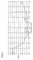
- a relationship between the frequency and the VSWR is shown in Fig. 29.
- Fig. 28 demonstrates that the track of the impedance of the antenna element according to the present invention concentrates near the central point of the Smith chart.
- the reflection coefficient of the antenna element is small. Since points 211-214 are positioned near the central point of the Smith chart, the reflection coefficient is particularly small in this band.
- antenna element 1a according to the present invention has a small reflection coefficient over a broad band.
- a broad band having frequencies of 1.57 GHz to 2.50 GHz a VSWR of 2 or less is given.
- the relative band width was obtained from Fig. 29, it was 46.5%.
- the antenna element according to the present invention had a VSWR of 2 or less in a broader band, as compared with the conventional antenna element. Therefore, the antenna element according to the present invention can be used in a broad band.
- a sample according to the present invention was prepared, in which a length of monopole antenna 14a was set to 115 mm (electric length: 7/8 ⁇ ) and the other structures had the same as the antenna element about which the data shown in Figs. 28 and 29 were collected.
- a radio wave having frequencies of 1.5 GHZ to 2.5 GHz was also introduced from feeding point 12 to this sample, and then the impedance, the Smith chart and the VSWR of the antenna element were obtained.
- Table 3 Point Frequency (GHz) Impedance of the antenna element ( ⁇ ) VSWR Real part( ⁇ ) Imaginary part( ⁇ ) 221 1.92 39.492 1.6641 1.2695 222 1.98 35.598 4.9961 1.4321 223 2.11 36.408 -3.5723 1.3871 224 2.17 28.409 -1.3828 1.7606
- the smith chart is shown in Fig. 30.
- a relationship between the frequency and the VSWR is shown in Fig. 31.
- Fig. 30 demonstrates that the track of the impedance of the product according to the present invention concentrates near the central point of the Smith chart. Since points 221-224 are positioned near the central point of the Smith chart, the reflection coefficient is particularly small in this band.
- the present invention product in a band having small frequencies the VSWR of the present invention product rose.
- the present invention product has a VSWR of 2 or less in a broader band, as compared with the conventional product.
- a VSWR of 2 or less is given.
- the relative band width was obtained from Fig. 31, it was 20%. It can be understood from the above that even if the length of monopole antenna 14a is changed, the present invention product has a broad usable band than the conventional product.
- a sample wherein antenna 114 illustrated in Fig. 25 was composed of a helical antenna was prepared as a conventional product.
- the pitch of the helical antenna was set to 3 mm.
- the electric length of the helical antenna was set to 3 ⁇ /8.
- Other circuit structures were made to the same as illustrated in Fig. 25.
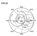
- the smith chart is shown in Fig. 32.
- a relationship between the frequency and the VSWR is shown in Fig. 33.
- Fig. 32 demonstrates that about the conventional product using the helical antenna, the track of the impedance thereof is largely out of the central point of the Smith chart even if the product has the matching circuit. About points 231-234 of middle frequencies as well as a point L of the smallest frequency and a point H of the largest frequency, the reflection coefficients thereof are large.
- a VSWR of 2 or less is given in the frequency range of 1.89 GHz to 1.97 GHz and in the frequency range of 2.12 GHz to 2.17 GHz. It can be understood that the band in which a VSWR of 2 or less is given is narrow. When the relative band width was obtained from Fig. 33, it was 6.5%.
- the conventional product in which the helical antenna is used has a narrow usable band.
- the conventional product is an antenna element which could be used as a high-efficiency antenna only in a small band.
- a product of the present invention having helical antenna 14b illustrated in Fig. 9 was prepared.
- the size of plate antenna 13 was made to the same size as the sample about which the data shown in Figs. 28 and 29 were collected.
- helical antenna 14b was made to the same as in the sample about which the data shown in Figs. 32 and 33 were collected.
- the smith chart is shown in Fig. 34.
- a relationship between the frequency and the VSWR is shown in Fig. 35.
- Fig. 34 demonstrates that the present invention product has large reflection coefficients at a point H of a high frequency and at a point L of a low frequency, as compared with the conventional product. However, points 241-244 of middle frequencies are near the central point of the Smith chart and thus the reflection coefficients are low.
- a VSWR of 2 or less is given in a broader band, as compared with the conventional product. Specifically, it can be understood that a VSWR of 2 or less is given in the frequency range of 1.66 GHz to 2.25 GHz. When the relative band width was obtained from Fig. 35, it was 31%.
- the antenna element according to the present invention can be used in the fields of, for example, a portable information terminal such as a portable telephone, an ordinary radio, a special radio, and a primary radiator of an aperture antenna such as a parabolic antenna.
Landscapes
- Engineering & Computer Science (AREA)
- Computer Networks & Wireless Communication (AREA)
- Details Of Aerials (AREA)
Abstract
Description
- This present invention relates to an antenna element and a portable information terminal, particularly to an antenna element used in a portable telephone and a portable telephone using the antenna.
- As an antenna element for transmission and reception in portable telephones, there has been hitherto known, for example, a monopole antenna or a helical antenna set up to extend in the longitudinal direction of their case.
- The impedance of such an antenna element is different from the impedance of a radio section inside the portable telephones. It is therefore necessary to match these impedances with each other. For this purpose, in conventional portable telephones, a matching circuit is arranged between their radio section and their antenna element.
- In recent years, a portable information terminal which can achieve two functions as a portable telephone and a personal handy-phone system (PHS) has been developed. A portable telephone and a PHS are different from each other in the radio frequencies (band) used for transmission and reception of information. In the case that information communication is carried out in any one band, an antenna is generally designed in the manner that the voltage standing wave ratio (VSWR) of the antenna is set to 2 or less in the band. It is therefore necessary that in the portable information terminal which can achieve two functions as a portable telephone and a PHS, the VSWR of its antenna is set to 2 or less in plural bands or a broad band. However, in conventional antennas having such a matching circuit as described above, the band in which the VSWR of the antennas is 2 or less is narrow. Thus, it is difficult that the conventional antennas are used as portable information terminals having the above-mentioned plural functions.
- The conventional matching circuit is composed of lumped-parameter elements such as a coil and a condenser. Therefore, when electrical signals are transmitted from a radio section to an antenna element through the matching circuit, loss is generated in the coil and condenser in the matching circuit to cause a problem that transmission efficiency of the electrical signals is lowered.
- Thus, the present invention has been made to overcome the above-mentioned problems.
- An object of the present invention is to provide an antenna element and a portable information terminal in which loss of electrical signals is small to give high efficiency.
- Another object of the present invention is to provide an antenna element and a portable information terminal having a broad usable band.
- The antenna element according to the present invention includes a first antenna part which is substantially equivalent to a series resonant circuit, and a second antenna part which is brought with contact with and connected to the first antenna part and is substantially equivalent to a parallel resonant circuit.
- In the antenna element having this structure, the first antenna part is substantially equivalent to the series resonant circuit and the second antenna part is substantially equivalent to the parallel resonant circuit. Therefore, the first antenna part and the second antenna part have impedance characteristics reverse to each other. By jointing the two antenna parts having the reverse impedance characteristics in above-mentioned way, their reactances are mutually cancelled out. In this way, the impedance of the antenna element and that of a radio section can be matched with each other so that a usable band can be made broad without using any matching circuit.
- Since the impedances can be matched with each other by jointing the two antenna parts, it is unnecessary to set a matching circuit as seen in the prior art. As a result, loss of electrical signals in the matching circuit can be prevented. Thus, the antenna element of the present invention has a high efficiency.
- Preferably, the first antenna part and the second antenna part are fitted in series to a feeding point.
- Preferably, the first antenna part and the second antenna part are fitted in parallel to a feeding point.
- Preferably, the first antenna part includes a plate antenna, and the second antenna part includes a linear antenna.
- Preferably, the linear antenna includes at least one selected from the group consisting of a monopole antenna and a helical antenna.
- Preferably, the antenna element further includes a substrate whose surface has an electrical conductivity; the first antenna part is set up, through a dielectric, over the surface of the substrate; and the second antenna part is set up to extend from the substrate.
- In this case, the first antenna part is set up, through the dielectric, over the surface of the substrate; therefore, the wavelength of a radio wave advancing in the first antenna part can be made short. As a result, the length of the first antenna part can be made short so that the size of the antenna element can be made small. The second antenna part is set up to extend from the substrate; therefore, the second antenna part can transmit and receive the radio wave certainly without being affected by the substrate.
- Preferably, the antenna element further includes a substrate whose surface has an electrical conductivity; and the first antenna part and the second antenna part are set up, through a dielectric, over the surface of the substrate. In this case, the first antenna part and the second antenna part are set up, through the dielectric, over the surface of the substrate; therefore, the wavelength of a radio wave advancing in the first and second antenna parts can be made short. As a result, the size of the first and second antenna parts can be made small so that the size of the antenna element can be made small.
- Preferably, the second antenna part includes at least one selected from the group consisting of a monopole antenna, a helical antenna, a meander line antenna, and a zigzag antenna.
- The portable information terminal according to the present invention includes an antenna element including a first antenna part which is substantially equivalent to a series resonant circuit, and a second antenna part which is brought with contact with and connected to the first antenna part and is substantially equivalent to a parallel resonant circuit.
- In the portable information terminal having this structure, the first antenna part is substantially equivalent to the series resonant circuit and the second antenna part is substantially equivalent to the parallel resonant circuit. Therefore, the first antenna part and the second antenna part have impedance characteristics reverse to each other. By jointing the two antenna parts having the reverse impedance characteristics, their reactances are mutually cancelled out. Thus, the impedance of the antenna element and that of a radio section can be matched with each other. As a result, the portable information terminal has a broad usable band.
- Since the impedances can be matched without using a matching circuit as seen in the prior art, loss of electrical signals in the matching circuit is not generated. Thus, the portable information terminal of the present invention has a high efficiency.
-
- Fig. 1 is a plan view of an antenna element according to a first embodiment of the present invention.
- Fig. 2 is a side view of the antenna element, as is viewed from the direction shown by an
arrow 11 in Fig. 1. - Fig. 3 is an equivalent circuit diagram of a plate antenna.
- Fig. 4 is a Smith chart for explaining the property of the plate antenna.
- Fig. 5 is an equivalent circuit diagram of a monopole antenna.
- Fig. 6 is a Smith chart for explaining the property of the monopole antenna.
- Fig. 7 is an equivalent circuit diagram of the antenna element illustrated in Figs. 1 and 2.
- Fig. 8 is a Smith chart for explaining the property of the antenna illustrated in Figs. 1 and 2.
- Fig. 9 is a plan view of an antenna element according to a second embodiment of the present invention.
- Fig. 10 is a plan view of an antenna element according to a third embodiment of the present invention.
- Fig. 11 is a plan view of an antenna element according to a fourth embodiment of the present invention.
- Fig. 12 is a plan view of an antenna element according to a fifth embodiment of the present invention.
- Fig. 13 is a plan view of an antenna element according to a sixth embodiment of the present invention.
- Fig. 14 is a plan view of an antenna element according to a seventh embodiment of the present invention.
- Fig. 15 is a plan view of an antenna element according to an eighth embodiment of the present invention.
- Fig. 16 is a plan view of an antenna element according to a ninth embodiment of the present invention.
- Fig. 17 is a plan view of an antenna element according to a tenth embodiment of the present invention.
- Fig. 18 is a plan view of an antenna element according to an eleventh embodiment of the present invention.
- Fig. 19 is a perspective view of an antenna element according to a twelfth embodiment of the present invention.
- Fig. 20 is a perspective view of an antenna element according to a thirteenth embodiment of the present invention and a portable telephone using this antenna element.
- Fig. 21 is a perspective view of an antenna element according to a fourteenth embodiment of the present invention and a portable telephone using this antenna element.
- Fig. 22 is a plan view of an antenna element according to a fifteenth embodiment of the present invention.
- Fig. 23 is an equivalent circuit diagram of the antenna element illustrated in Fig. 22.
- Fig. 24 is a Smith chart for explaining the property of the antenna element illustrated in Fig. 22.
- Fig. 25 is a circuit diagram of a conventional antenna element.
- Fig. 26 is a Smith chart for explaining the property of the conventional antenna element.
- Fig. 27 is a graph showing a relationship between frequency and VSWR in the conventional antenna element.
- Fig. 28 is a Smith chart for explaining the property of an antenna element of the present invention.
- Fig. 29 is a graph showing a relationship between frequency and VSWR in the antenna element of the present invention.
- Fig. 30 is a Smith chart for explaining the property of an antenna element of the present invention.
- Fig. 31 is a graph showing a relationship between frequency and VSWR in the antenna element of the present invention.
- Fig. 32 is a Smith chart for explaining the property of a conventional antenna element.
- Fig. 33 is a graph showing a relationship between frequency and VSWR in the conventional antenna element.
- Fig. 34 is a Smith chart for explaining the property of an antenna element of the present invention.
- Fig. 35 is a graph showing a relationship between frequency and VSWR in the antenna element of the present invention.
- Referring to the drawings, embodiments of the present invention will be described hereinafter.
- Fig. 1 is a plan view of an antenna element according to the first embodiment of the present invention. Referring to Fig. 1, an
antenna element 1a has aplate antenna 13 as a first antenna part which is substantially equivalent to a series resonant circuit, amonopole antenna 14a as a second antenna part which is connected to plateantenna 13 and is substantially equivalent to a parallel resonant circuit, and ametal substrate 11 as a base plate. -
Plate antenna 13 is composed of a microstrip line. The electric length ofplate antenna 13 is about λ/4. Afeeding point 12 is connected to one end ofplate antenna 13.Feeding point 12 is a point which is connected to a given radio section. The radio section andplate antenna 13 are connected to each other throughfeeding point 12.Monopole antenna 14a is connected to the other end ofplate antenna 13. -
Monopole antenna 14a is formed to extend in the longitudinal direction ofmetal substrate 11.Monopole antenna 14a andplate antenna 13 are fitted in series tofeeding point 12. The electric length ofmonopole antenna 14a is about 3λ/8. Thismonopole antenna 14a has the so-called anti-resonance characteristic.Monopole antenna 14a andplate antenna 13 fulfill functions for transmission and reception of radio waves. -
Metal substrate 11 is formed by depositing a metal layer (for example, a copper layer) on a given insulating substrate. The metal layer deposited on the insulating substrate has an electric conductivity which is substantially equal to that of copper.Metal substrate 11 is substantially rectangular. Long sides thereof are along the direction in whichmonopole antenna 14a extends. - Fig. 2 is a side view of the antenna element, as is viewed from the direction shown by an arrow II in Fig. 1. Referring to Fig. 2,
antenna element 1a hasmetal substrate 11,plate antenna 13 andmonopole antenna 14a.Metal substrate 11 is in the form of a thin plate and is formed so as to extend in one direction. The radio section (not illustrated) is fitted up ontometal substrate 11. This radio section is connected to plateantenna 13 throughfeeding point 12.Plate antenna 13 is in an L-shaped member. One end ofplate antenna 13 is connected to feedingpoint 12. The other end thereof is connected tomonopole antenna 14a. A dielectric 15 is inserted betweenplate antenna 13 andmetal substrate 11.Dielectric 15 is made of Teflon (relative dielectric constant: 2.1).Plate antenna 13 is made of copper. - Fig. 3 is an equivalent circuit diagram of the plate antenna. Fig. 4 is a Smith chart for explaining the property of the plate antenna. Referring to Fig. 3,
plate antenna 13 is substantially equivalent to a seriesresonant circuit 20a wherein aresistance 21, acoil 22 and acondenser 23 are connected in series tofeeding point 12. - Referring to Fig. 4, about frequencies higher than frequencies near a resonance point, the imaginary part of the impedance of the plate antenna is positive as shown at a point H since this antenna is substantially equivalent to the series resonant circuit as illustrated in Fig. 3. On the other hand, about frequencies lower than the frequencies near the resonance point, the imaginary part of the impedance is negative as shown at a point L.
- Fig. 5 is an equivalent circuit diagram of the monopole antenna. Fig. 6 is a Smith chart for explaining the property of the monopole antenna. Referring to Fig. 5, the monopole antenna is substantially equivalent to a parallel
resonant circuit 20b wherein aresistance 21, acoil 22 and acondenser 23 are connected in parallel to feedingpoint 12. Referring to Fig. 6, about frequencies higher than frequencies near a resonance point, the imaginary part of the impedance ofmonopole antenna 14a is negative. On the other hand, about frequencies lower than the frequencies near the resonance point, the imaginary part of the impedance is positive as shown at a point L. - Fig. 7 is an equivalent circuit diagram of the antenna element illustrated in Figs. 1 and 2. Referring to Fig. 7,
antenna element 1a is equivalent to a circuit wherein seriesresonant circuit 20a and parallelresonant circuit 20b are jointed to each other. Fig. 8 is a Smith chart for explaining the property of the antenna illustrated in Figs. 1 and 2. Referring to Fig. 8, the Smith chart of the antenna according to the present invention is a synthesis of the Smith chart of the plate antenna, shown in Fig. 4, and the Smith chart of the monopole antenna, shown in Fig. 6. That is, the imaginary part of the impedance is negative to the radio wave having the highest frequency, shown at a point H. However, the reflection coefficient (the distance from the center of the Smith chart to point H) to the radio wave shown at point H in Fig. 8 is smaller than the reflection coefficient at point H in Figs. 4 and 6. As the frequency becomes smaller, the track of the impedance is nearer to the central point. Thus, at an intermediate point M of the frequency, the imaginary part of the impedance is zero. When the frequency is made smaller, the track of the impedance is shifted to be away from the central point. Thus, the track reaches a point L having the smallest frequency. The reflection coefficient at point L in Fig. 8 is smaller than that at points L shown in Figs. 4 and 6. - In Fig. 8, series
resonant circuit 20a and parallelresonant circuit 20b are connected to each other. Therefore, each of the two circuits cancels the property of the opponent circuit. As a result, the reflection coefficient is small over a broad band. In other words, the track of the impedance of the present invention concentrates nearer to the central point, as compared with conventional monopole antennas and plate antennas, so that an antenna having a broad usable band can be produced. Since the impedance approaches 50 Ω, the impedance of the antenna and that of the radio section can be matched with each other without setting up any conventional matching circuit. As a result, a matching element can be omitted so that loss of electric signals based on the matching element can be prevented. - The electric length of
monopole antenna 14a can be made to an electric length represented by 3λ/8 + (λ/2) × N, wherein N is an integer, and having anti-resonance characteristic. The electric length ofplate antenna 13 can be made to an electric length represented by λ/4 + (λ/2) × N, wherein N is an integer, and having resonance characteristic. In the above-mentioned example,plate antenna 13 andmonopole antenna 14a are set up over one surface ofmetal substrate 11, butplate antennas 13 andmonopole antennas 14a may be set up over both surfaces ofmetal substrate 11. - Fig. 9 is a plan view of an antenna element according to the second embodiment of the present invention. Referring to Fig. 9, an
antenna element 1b according to the second embodiment is different fromantenna element 1a illustrated in Figs. 1 and 2 in thatantenna element 1b has ahelical antenna 14b as the second antenna part. -
Helical antenna 14b generally has a narrow usable band. According to the present invention, even ifhelical antenna 14b is used, an antenna element having a broad usable band can be produced. - By using
helical antenna 14b, the physical length of the antenna element can be made small. - Fig. 10 is a plan view of an antenna element according to the third embodiment of the present invention. Referring to Fig. 10, an
antenna element 1c according to the third embodiment is different fromantenna element 1a illustrated in Figs. 1 and 2, wherein onlymonopole antenna 14a is set up as the first antenna part, in that amonopole antenna 14a and ahelical antenna 14b are set up as the first antenna part. -
Antenna element 1c having the above-mentioned structure also has the same advantages as the antenna element illustrated in Fig. 1. Furthermore, by combiningmonopole antenna 14a withhelical antenna 14b, properties dependently on use or purposes can be exhibited. - Fig. 11 is a plan view of an antenna element according to the fourth embodiment of the present invention. Referring to Fig. 11, an
antenna element 1d according to the fourth embodiment is different fromantenna element 1a illustrated in Figs. 1 and 2, whereinmonopole antenna 14a is set up to extend frommetal substrate 11, in that ameander line antenna 14d is used as the first antenna part and thismeander line antenna 14d is set up onmetal substrate 11. -
Meander line antenna 14d is set up to interpose air betweenantenna 14d andmetal substrate 11. One end ofantenna 14d is connected to aplate antenna 13. -
Antenna element 1d having the above-mentioned structure also has the same advantages asantenna element 1a illustrated in Figs. 1 and 2. Furthermore, an antenna, such asmonopole antenna 14a illustrated in Figs. 1 and 2, does not project frommetal substrate 11 sincemeander line antenna 14d is made onmetal substrate 11. As a result, the whole ofantenna element 1d can be made thin and small. - Fig. 12 is a plan view of an antenna element according to the fifth embodiment of the present invention. Referring to Fig. 12, an
antenna element 1e according to the fifth embodiment is different fromantenna element 1d illustrated in Fig. 11, which hasmeander line antenna 14d as the second antenna part, in thatantenna element 1e has ahelical antenna 14e as the second antenna part. -
Antenna element 1e having the above-mentioned structure also has the same advantages asantenna element 1d illustrated in Fig. 11. - Fig. 13 is a plan view of an antenna element according to the sixth embodiment of the present invention. Referring to Fig. 13, an
antenna element 1f according to the sixth embodiment is different fromantenna element 1d illustrated in Fig. 11, which hasmeander line antenna 14d as the second antenna part, in that antenna element if has azigzag antenna 14f as the second antenna part. -
Antenna element 1f having the above-mentioned structure also has the same advantages asantenna element 1d illustrated in Fig. 11. - Fig. 14 is a plan view of an antenna element according to the seventh embodiment of the present invention. Referring to Fig. 14, an
antenna element 1g according to the seventh embodiment is different fromantenna element 1d illustrated in Fig. 11, which hasmeander line antenna 14d as the second antenna, in thatantenna element 1g has amonopole antenna 14g as the second antenna. -
Antenna element 1g having the above-mentioned structure also has the same advantages asantenna element 1d illustrated in Fig. 11. - Fig. 15 is a plan view of an antenna element according to the eighth embodiment of the present invention. Referring to Fig. 15, an
antenna element 1h according to the eighth embodiment is different fromantenna element 1d illustrated in Fig. 11, which has no dielectric 18, in that a dielectric 18 is formed on ametal substrate 11 and aplate antenna 13 and ameander line antenna 14d are formed ondielectric 18. -
Dielectric 18 is made of a material having a small dielectric tangent tan δ and a high relative dielectric constant, for example, a ceramic material(relative dielectric constant ≒ 7-100), Teflon (relative dielectric constant ≒ 2.1) or a resin material (relative dielectric constant ≒ 3.3) such as Vectra. -
Antenna element 1h having the above-mentioned structure has the same advantages asantenna element 1d illustrated in Fig. 11. Sinceplate antenna 13 andmeander line antenna 14d are put on dielectric 18 having a high relative dielectric constant, the wavelength of a radio wave advancing inplate antenna 13 andmeander line antenna 14d can be made short. As a result, the size ofplate antenna 13 andmeander line antenna 14d can be made small. The size ofmetal substrate 11 can also be made small. - Fig. 16 is a plan view of an antenna element according to the ninth embodiment of the present invention. Referring to Fig. 16, an
antenna element 1i according to the ninth embodiment is different fromantenna element 1h illustrated in Fig. 15 in thatantenna element 1i has ahelical antenna 14e as the second antenna part. -
Antenna element 1i having the above-mentioned structure has the same advantages asantenna element 1h illustrated in Fig. 15. - Fig. 17 is a plan view of an antenna element according to the tenth embodiment of the present invention. Referring to Fig. 17, an
antenna element 1j according to the tenth embodiment is different fromantenna element 1h illustrated in Fig. 15 in thatantenna element 1j has azigzag antenna 14f as the second antenna part. -
Antenna element 1j having the above-mentioned structure has the same advantages asantenna element 1h illustrated in Fig. 15. - Fig. 18 is a plan view of an antenna element according to the eleventh embodiment of the present invention. Referring to Fig. 18, an
antenna element 1k according to the eleventh embodiment is different fromantenna element 1h illustrated in Fig. 15 in thatantenna element 1k has amonopole antenna 14g as the second antenna. -
Antenna element 1k having the above-mentioned structure also has the same advantages asantenna element 1h illustrated in Fig. 15. - Fig. 19 is a perspective view of an antenna element according to the twelfth embodiment of the present invention. Referring to Fig. 19, an
antenna element 1m according to the twelfth embodiment has ametal substrate 11, aplate member 19, aplate antenna 13, and ameander line antenna 14d.Plate member 19 is fixed tometal substrate 11.Plate member 19 has a structure wherein a dielectric and a metal plate overlap with each other.Plate member 19 is fitted perpendicularly tometal substrate 11. Therefore,metal substrate 11 andplate member 19 are jointed to each other to form an L-shaped base plate.Plate member 19 is set up on the top face ofmetal substrate 11. -
Plate antenna 13 andmeander line antenna 14d are made onplate member 19.Plate antenna 13 is connected to afeeding point 12.Plate antenna 13 andmeander line antenna 14d spread to extend in the direction perpendicular to the main face ofmetal substrate 11. -
Antenna element 1m having the above-mentioned structure has the same advantages asantenna element 1a illustrated in Figs. 1 and 2. - Furthermore, the length of the longitudinal direction of
metal substrate 11 can be made short sinceplate antenna 13 andmeander line antenna 14d are put onplate member 19 set up perpendicularly tometal substrate 11. For this reason, the size ofmetal substrate 11 can be made small and the area for mounting the antenna element can be made small. - Fig. 20 is a perspective view of an antenna element according to the thirteenth embodiment of the present invention and a portable telephone using this antenna element. Referring to Fig. 20, a
portable telephone 50a according to the present invention has anantenna element 1n and arear case 32 for storing this antenna element. -
Antenna element 1n has aplate antenna 13 as a first antenna part, amonopole antenna 14a as a second antenna part, and ametal substrate 11 as a base plate.Plate antenna 13 andmonopole antenna 14a are fixed torear case 32.Plate antenna 13 is set inrear case 32, andmonopole antenna 14a is set to project fromrear case 32.Plate antenna 13 andmonopole antenna 14a are connected to each other. Afeeding point 12 is set onmetal substrate 11.Feeding point 12 is connected to one end ofplate antenna 13 through ametal pin 31.Metal substrate 11 is also stored inrear case 32. A non-illustrated radio section is made onmetal substrate 11. -
Antenna element 1n having the above-mentioned structure has the same constitution asantenna element 1a illustrated in Figs. 1 and 2, so as to have the same advantages asantenna element 1a illustrated in Figs. 1 and 2. - Furthermore,
portable telephone 50a according to the present invention has a broad usable band since it hasantenna element 1h. Thus,telephone 50a makes it possible to transmit and receive radio waves having broad frequencies. As a result, for example, two functions of PHS and a portable telephone can be fulfilled. - Since this antenna element has no matching circuit, loss of electric signals by a matching circuit is not generated.
- At the time of production, precision can be made high.
- Fig. 21 is a perspective view of an antenna element according to the fourteenth embodiment of the present invention and a portable telephone using this antenna element. Referring to Fig. 21, a
portable telephone 50b according to the present invention has anantenna element 1p and arear case 32.Antenna element 1p is different fromantenna element 1n illustrated in Fig. 20, which has no contact spring, in thatantenna element 1p has a contact spring 34 which also functions as an antenna at one end of aplate antenna 13. Contact spring 34 is connected to afeeding point 12. -
Antenna element 1p having the above-mentioned structure has the same advantages asantenna element 1n illustrated in Fig. 20. - Furthermore,
portable telephone 50b using thisantenna element 1p has a broad usable band and gives a small loss in the same way asportable telephone 50a illustrated in Fig. 20. - The number of the parts also becomes small.
- Fig. 22 is a plan view of an antenna element according to the fifteenth embodiment of the present invention. Referring to Fig. 22, an
antenna element 1q has amonopole antenna 14a as a first antenna part, aplate antenna 13 as a second antenna part, and ametal substrate 11. -
Plate antenna 13 is put onmetal substrate 11.Monopole antenna 14a is set up to extend frommetal substrate 11.Monopole antenna 14a andplate antenna 13 are connected in parallel to afeeding point 12. As described about the above-mentioned embodiment,monopole antenna 14a may be substituted with the above-mentionedhelical antenna zigzag antenna 14f,meander line antenna 14d,monopole antenna 14g or the like.Monopole antenna 14a may be put onmetal substrate 11. A material having a high dielectric constant may be interposed betweenmonopole antenna 14a,plate antenna 13 andmetal substrate 11. - Fig. 23 is an equivalent circuit diagram of the antenna element illustrated in Fig. 22. Referring to Fig. 23,
plate antenna 13 is substantially equivalent to a seriesresonant circuit 20a wherein aresistance 21, acoil 22 and acondenser 23 are connected in series to each other.Monopole antenna 14a is substantially equivalent to a parallelresonant circuit 20b wherein aresistance 21, acoil 22 and acondenser 23 are connected in parallel to each other. The two circuits are jointed to each other. - Fig. 24 is a Smith chart for explaining the impedance property of the antenna element illustrated in Fig. 22. Referring to Fig. 24, about radio waves having a high frequency, the imaginary part of the impedance of
antenna element 1q is positive as shown at a point H. As its frequency becomes lower, the imaginary part of the impedance approaches zero. Furthermore, the track of the impedance moves to surround the central point of the Smith chart. As the frequency is made lower, the imaginary part of the impedance becomes negative. As shown at a point L, when the frequency is smallest, the imaginary part of the impedance is most negative so that the track is apart from the central point of the Smith chart. - The Smith chart shown in Fig. 24 is compared with the Smith charts of the plate antenna and the monopole antenna shown in Figs. 4 and 6. In the Smith chart shown in Fig. 24, the distance between points H & L and the center of the chart is shorter than the distance between points H & L of in the Smith chart shown in Figs. 4 and 6 and the center of this chart. This is because series
resonant circuit 20a and parallelresonant circuit 20b have different properties and the circuits are jointed to each other so that their properties are mutually cancelled out. In this manner, impedance-matching is attained. - It can be understood that most of the track of the impedance is present near the center of the Smith chart so that the reflection coefficient of
antenna element 1q is small. As a result,antenna element 1q has a small reflection coefficient over a broad band so thatelement 1q can be used in the broad band. - Impedance-matching can be attained without using any matching circuit. Therefore, loss of electrical signals in a matching circuit, as is conventionally seen, is not generated.
- Specific examples of the present invention will be described hereinafter.
- Fig. 25 is a circuit diagram of a conventional antenna element. Referring to Fig. 25, the antenna element was composed of an
antenna 114, acoil 122, astub 124 and acondenser 123.Coil 122 has an inductance of 6.8 nH.Condenser 123 has a capacity of 4 pF.Antenna 114 is composed of a monopole antenna and has a length of 55 mm (electric length: 3λ/8). A radio wave having frequencies of 1.5 GHz to 2.5 GHz was inputted to the antenna element having the above-mentioned matching circuit, and then the impedance, the Smith chart and the VSWR of the antenna element were examined. About specified points, the impedance and the VSWR thereof are shown in Table 1.Table 1 Point Frequency
(GHz)Impedance of the antenna element
having the matching circuit(Ω)VSWR Real part(Ω) Imaginary part(Ω) 201 1.92 58 0 1.2 202 1.98 44 3 1.3 203 2.11 48 14 1.4 204 2.17 48 -10 1.4 - The smith chart is shown in Fig. 26. A relationship between the frequency and the VSWR is shown in Fig. 27.
- The Smith chart shown in Fig. 26 demonstrates that the reflection coefficient of the conventional antenna element was large in a band having high frequencies and a band having low frequencies. On the other hand, as shown at points 201-204, the reflection coefficient was small in the frequency range of 1.9 GHz to 2.2 GHz.
- Fig. 27 demonstrates that the band in which a VSWR of 2 or less was given was a band having a frequency of 1.84 GHz to 2.20 GHz. The relative band width was 18%. In the specification, the "relative band width" means a relative band width about the band in which a VSWR of 2 or less is given. The relative band width can be obtained by the following equation:

- From the above, it can be understood that the conventional antenna element was an antenna element having a narrow relative band width even if the antenna element had the matching circuit.
- As a product of the present invention, the
antenna element 1a illustrated in Figs. 1 and 2 was prepared. In thisantenna element 1a, lengths W1 and W2 of sides ofplate antenna 13 were set to 0.03λ and 0.04λ. Thickness (electric length) H of dielectric 15 made of Teflon (relative dielectric constant: 2.1) was set to 0.015λ. The length ofmonopole antenna 14a was set to 50 mm (electric length: 3λ/8). - A radio wave having frequencies of 1.5 GHZ to 2.5 GHz was introduced from feeding
point 12 toantenna element 1a, and then the impedance, the Smith chart and the VSWR of theantenna element 1a were obtained. About specified points, the impedance and the VSWR thereof are shown in Table 2.Table 2 Point Frequency
(GHz)Impedance of the antenna element (Ω) VSWR Real part(Ω) Imaginary part(Ω) 211 1.92 38.881 -7.9688 1.3617 212 1.98 43.418 0.7422 1.1525 213 2.11 49.703 -12.436 1.282 214 2.17 43.465 -16.473 1.4583 - The smith chart is shown in Fig. 28. A relationship between the frequency and the VSWR is shown in Fig. 29.
- Fig. 28 demonstrates that the track of the impedance of the antenna element according to the present invention concentrates near the central point of the Smith chart. Thus, the reflection coefficient of the antenna element is small. Since points 211-214 are positioned near the central point of the Smith chart, the reflection coefficient is particularly small in this band.
- It can be understood from the above-mentioned results that
antenna element 1a according to the present invention has a small reflection coefficient over a broad band. As shown in Fig. 29, in a broad band having frequencies of 1.57 GHz to 2.50 GHz a VSWR of 2 or less is given. When the relative band width was obtained from Fig. 29, it was 46.5%. - From the above, it can be understood that the antenna element according to the present invention had a VSWR of 2 or less in a broader band, as compared with the conventional antenna element. Therefore, the antenna element according to the present invention can be used in a broad band.
- Next, a sample according to the present invention was prepared, in which a length of
monopole antenna 14a was set to 115 mm (electric length: 7/8λ) and the other structures had the same as the antenna element about which the data shown in Figs. 28 and 29 were collected. A radio wave having frequencies of 1.5 GHZ to 2.5 GHz was also introduced from feedingpoint 12 to this sample, and then the impedance, the Smith chart and the VSWR of the antenna element were obtained. - About specified points, the impedance and the VSWR thereof are shown in Table 3.
Table 3 Point Frequency
(GHz)Impedance of the antenna element (Ω) VSWR Real part(Ω) Imaginary part(Ω) 221 1.92 39.492 1.6641 1.2695 222 1.98 35.598 4.9961 1.4321 223 2.11 36.408 -3.5723 1.3871 224 2.17 28.409 -1.3828 1.7606 - The smith chart is shown in Fig. 30. A relationship between the frequency and the VSWR is shown in Fig. 31.
- Fig. 30 demonstrates that the track of the impedance of the product according to the present invention concentrates near the central point of the Smith chart. Since points 221-224 are positioned near the central point of the Smith chart, the reflection coefficient is particularly small in this band.
- Referring to Fig. 31, in a band having small frequencies the VSWR of the present invention product rose. However, the present invention product has a VSWR of 2 or less in a broader band, as compared with the conventional product. As shown in Fig. 31, in a band having frequencies of 1.83 GHz to 2.22 GHz a VSWR of 2 or less is given. When the relative band width was obtained from Fig. 31, it was 20%. It can be understood from the above that even if the length of
monopole antenna 14a is changed, the present invention product has a broad usable band than the conventional product. - The following will describe an example in which a helical antenna is used. First, a sample wherein
antenna 114 illustrated in Fig. 25 was composed of a helical antenna was prepared as a conventional product. The pitch of the helical antenna was set to 3 mm. The electric length of the helical antenna was set to 3λ/8. Other circuit structures were made to the same as illustrated in Fig. 25. - A radio wave having frequencies of 1.5 GHZ to 2.5 GHz was also introduced to this sample, and then the impedance, the Smith chart and the VSWR of the antenna element were obtained. About specified points, the impedance and the VSWR thereof are shown in Table 4.
Table 4 Point Frequency
(GHz)Impedance of the antenna element
having the matching circuit(Ω)VSWR Real part(Ω) Imaginary part(Ω) 231 1.92 58 -30 1.8 232 1.98 24 -3 2.1 233 2.11 60 30 2.1 234 2.17 48 -28 2.0 - The smith chart is shown in Fig. 32. A relationship between the frequency and the VSWR is shown in Fig. 33.
- Fig. 32 demonstrates that about the conventional product using the helical antenna, the track of the impedance thereof is largely out of the central point of the Smith chart even if the product has the matching circuit. About points 231-234 of middle frequencies as well as a point L of the smallest frequency and a point H of the largest frequency, the reflection coefficients thereof are large.
- Referring to Fig. 33, a VSWR of 2 or less is given in the frequency range of 1.89 GHz to 1.97 GHz and in the frequency range of 2.12 GHz to 2.17 GHz. It can be understood that the band in which a VSWR of 2 or less is given is narrow. When the relative band width was obtained from Fig. 33, it was 6.5%.
- As described above, the conventional product in which the helical antenna is used has a narrow usable band. Thus, it can be understood that the conventional product is an antenna element which could be used as a high-efficiency antenna only in a small band.
- Next, a product of the present invention having
helical antenna 14b illustrated in Fig. 9 was prepared. The size ofplate antenna 13 was made to the same size as the sample about which the data shown in Figs. 28 and 29 were collected. Furthermore,helical antenna 14b was made to the same as in the sample about which the data shown in Figs. 32 and 33 were collected. - A radio wave having frequencies of 1.5 GHZ to 2.5 GHz was also introduced to this sample, and then the impedance, the Smith chart and the VSWR were obtained. About specified points, the impedance and the VSWR thereof are shown in Table 5.
Table 5 Point Frequency
(GHz)Impedance of the antenna element (Ω) VSWR Real part(Ω) Imaginary part(Ω) 241 1.92 33.908 -3.2734 1.4857 242 1.98 32.09 4.4355 1.5784 243 2.11 32.586 12.148 1.6805 244 2.17 33.92 17.066 1.7524 - The smith chart is shown in Fig. 34. A relationship between the frequency and the VSWR is shown in Fig. 35.
- Fig. 34 demonstrates that the present invention product has large reflection coefficients at a point H of a high frequency and at a point L of a low frequency, as compared with the conventional product. However, points 241-244 of middle frequencies are near the central point of the Smith chart and thus the reflection coefficients are low.
- Referring to Fig. 35, in the present invention product a VSWR of 2 or less is given in a broader band, as compared with the conventional product. Specifically, it can be understood that a VSWR of 2 or less is given in the frequency range of 1.66 GHz to 2.25 GHz. When the relative band width was obtained from Fig. 35, it was 31%.
- As described above, according to the present invention, it is possible to obtain an antenna element and a portable information terminal having a broad usable band and giving a small loss.
- The antenna element according to the present invention can be used in the fields of, for example, a portable information terminal such as a portable telephone, an ordinary radio, a special radio, and a primary radiator of an aperture antenna such as a parabolic antenna.
Claims (9)
- An antenna element, comprising a first antenna part (13) which is substantially equivalent to a series resonant circuit (20a), and a second antenna part (14a, 14b, 14d, 14e, 14f, 14g) which is brought with contact with and connected to said first antenna part (13) and is substantially equivalent to a parallel resonant circuit (20b).
- The antenna element according to claim 1, wherein said first antenna part (13) and said second antenna part (14a, 14b, 14d, 14e, 14f, 14g) are fitted in series to a feeding point (12).
- The antenna element according to claim 1, wherein said first antenna part (13) and said second antenna part (14a, 14b, 14d, 14e, 14f, 14g) are fitted in parallel to a feeding point (12).
- The antenna element according to claim 1, wherein the first antenna part comprises a plate antenna (13), and said second antenna part comprises a linear antenna (14a, 14b).
- The antenna element according to claim 4, wherein said linear antenna comprises at least one selected from the group consisting of a monopole antenna (14a) and a helical antenna (14b).
- The antenna element according to claim 1, which further comprises a substrate (11) whose surface has an electrical conductivity,
said first antenna part (13) being set up, through a dielectric (15), over the surface of said substrate (11), and
said second antenna part (14a, 14b) being set up to extend from said substrate (11). - The antenna element according to claim 1, which further comprises a substrate (11) whose surface has an electrical conductivity,
said first antenna part and second antenna part (13, 14d, 14e, 14f, 14g) being set up, through a dielectric (18), over the surface of said substrate (11). - The antenna element according to claim 7, wherein said second antenna part comprises at least one selected from the group consisting of a monopole antenna (14g), a helical antenna (14e), a meander line antenna (14d), and a zigzag antenna (14f).
- A portable information terminal, comprising an antenna element (1a, 1b, 1c, 1d, 1e, 1f, 1g, 1h, 1i, 1j, 1k, 1m, 1n, 1p, 1q) comprising a first antenna part (13) which is substantially equivalent to a series resonant circuit (20a), and a second antenna part (14a, 14b, 14d, 14e, 14f, 14g) which is connected to said first antenna part (13) and is substantially equivalent to a parallel resonant circuit (20b).
Applications Claiming Priority (1)
| Application Number | Priority Date | Filing Date | Title |
|---|---|---|---|
| PCT/JP2000/002428 WO2001080367A1 (en) | 2000-04-13 | 2000-04-13 | Antenna element and portable communication terminal |
Publications (2)
| Publication Number | Publication Date |
|---|---|
| EP1280233A1 true EP1280233A1 (en) | 2003-01-29 |
| EP1280233A4 EP1280233A4 (en) | 2004-12-22 |
Family
ID=11735919
Family Applications (1)
| Application Number | Title | Priority Date | Filing Date |
|---|---|---|---|
| EP00915521A Withdrawn EP1280233A4 (en) | 2000-04-13 | 2000-04-13 | ANTENNA ELEMENT AND PORTABLE COMMUNICATION TERMINAL |
Country Status (4)
| Country | Link |
|---|---|
| US (1) | US6670924B1 (en) |
| EP (1) | EP1280233A4 (en) |
| CN (1) | CN1370342A (en) |
| WO (1) | WO2001080367A1 (en) |
Cited By (2)
| Publication number | Priority date | Publication date | Assignee | Title |
|---|---|---|---|---|
| EP1643591A4 (en) * | 2003-07-04 | 2006-08-02 | Mitsubishi Electric Corp | ANTENNA ELEMENT AND MOBILE TELEPHONE |
| EP2306589A1 (en) * | 2009-10-05 | 2011-04-06 | Research In Motion Limited | Mobile communication device with a matched dual band antenna |
Families Citing this family (6)
| Publication number | Priority date | Publication date | Assignee | Title |
|---|---|---|---|---|
| GB2383470B (en) * | 2001-11-12 | 2004-04-28 | Transense Technologies Plc | Self contained radio apparatus for transmission of data |
| KR20040067906A (en) * | 2003-01-21 | 2004-07-30 | 소니 가부시끼 가이샤 | Flat antenna, antenna unit and broadcast reception terminal apparatus |
| JP4734383B2 (en) * | 2008-07-31 | 2011-07-27 | 株式会社東芝 | Broadband antenna |
| TWI404264B (en) * | 2009-09-02 | 2013-08-01 | Mstar Semiconductor Inc | Multi-band antenna apparatus |
| WO2014181569A1 (en) * | 2013-05-10 | 2014-11-13 | 株式会社村田製作所 | Antenna apparatus |
| CN114447574B (en) * | 2020-11-04 | 2025-02-25 | 富泰京精密电子(烟台)有限公司 | Antenna structure and wireless communication device having the same |
Family Cites Families (24)
| Publication number | Priority date | Publication date | Assignee | Title |
|---|---|---|---|---|
| GB929871A (en) * | 1958-08-06 | 1963-06-26 | Emi Ltd | Improvements relating to aerials |
| SE435435B (en) * | 1983-02-16 | 1984-09-24 | Ericsson Telefon Ab L M | ANTENNA SYSTEM ATTENTION |
| JPS6187434A (en) * | 1984-10-04 | 1986-05-02 | Nec Corp | Portable radio equipment |
| JPS6234407A (en) * | 1985-08-07 | 1987-02-14 | Fujitsu Ltd | Antenna for radio equipment |
| US5262792A (en) * | 1991-09-11 | 1993-11-16 | Harada Kogyo Kabushiki Kaisha | Shortened non-grounded type ultrashort-wave antenna |
| JP3223479B2 (en) | 1993-09-24 | 2001-10-29 | 三省電機株式会社 | Retractable antenna device for mobile communication equipment |
| JPH0878929A (en) | 1994-08-30 | 1996-03-22 | Sansei Denki Kk | Method for connecting antenna for mobile communication equipment and structure therefor |
| JPH09181512A (en) | 1995-12-25 | 1997-07-11 | Sansei Denki Kk | Method for connecting antenna for mobile communication equipment and its connection structure |
| JP3344688B2 (en) | 1996-09-02 | 2002-11-11 | 三省電機株式会社 | Method of connecting antenna to portable radio, and connection mechanism of antenna for portable radio |
| JP3441316B2 (en) * | 1996-10-31 | 2003-09-02 | 京セラ株式会社 | Common antenna device |
| JP3763032B2 (en) | 1997-04-23 | 2006-04-05 | 三省電機株式会社 | Extendable and fully retractable antenna support / connection method and apparatus |
| SE511501C2 (en) * | 1997-07-09 | 1999-10-11 | Allgon Ab | Compact antenna device |
| JPH11177331A (en) | 1997-12-15 | 1999-07-02 | Sansei Denki Kk | Dual band store type antenna and its construction method |
| JP3438016B2 (en) * | 1998-03-03 | 2003-08-18 | 株式会社ケンウッド | Multi-frequency resonant inverted-F antenna |
| JPH11261318A (en) | 1998-03-12 | 1999-09-24 | Sansei Denki Kk | Method for switching and using two antenna elements and switching type antenna system |
| US6288680B1 (en) * | 1998-03-18 | 2001-09-11 | Murata Manufacturing Co., Ltd. | Antenna apparatus and mobile communication apparatus using the same |
| SE518868C2 (en) * | 1998-03-19 | 2002-12-03 | Smarteq Wireless Ab | Antenna device with magnetic attachment device and earth connection means for operation at multiple frequencies |
| SE9801381D0 (en) * | 1998-04-20 | 1998-04-20 | Allgon Ab | Ground extension arrangement for coupling to ground means in an antenna system, and an antenna system and a mobile radio device having such ground arrangement |
| JPH11308038A (en) * | 1998-04-20 | 1999-11-05 | Yokowo Co Ltd | Antenna and antenna device |
| US6326924B1 (en) * | 1998-05-19 | 2001-12-04 | Kokusai Electric Co., Ltd. | Polarization diversity antenna system for cellular telephone |
| US6211830B1 (en) * | 1998-06-10 | 2001-04-03 | Matsushita Electric Industrial Co., Ltd. | Radio antenna device |
| JP2000151244A (en) | 1998-11-11 | 2000-05-30 | Sansei Denki Kk | Method for constructing collinear antenna for portable radio equipment and supporting device |
| US6137446A (en) * | 1999-02-17 | 2000-10-24 | Msx, Inc. | Method and apparatus for modulating voltage to an antenna reflector heater |
| US6198442B1 (en) * | 1999-07-22 | 2001-03-06 | Ericsson Inc. | Multiple frequency band branch antennas for wireless communicators |
-
2000
- 2000-04-13 US US10/009,495 patent/US6670924B1/en not_active Expired - Fee Related
- 2000-04-13 CN CN00811681.4A patent/CN1370342A/en active Pending
- 2000-04-13 EP EP00915521A patent/EP1280233A4/en not_active Withdrawn
- 2000-04-13 WO PCT/JP2000/002428 patent/WO2001080367A1/en not_active Ceased
Cited By (2)
| Publication number | Priority date | Publication date | Assignee | Title |
|---|---|---|---|---|
| EP1643591A4 (en) * | 2003-07-04 | 2006-08-02 | Mitsubishi Electric Corp | ANTENNA ELEMENT AND MOBILE TELEPHONE |
| EP2306589A1 (en) * | 2009-10-05 | 2011-04-06 | Research In Motion Limited | Mobile communication device with a matched dual band antenna |
Also Published As
| Publication number | Publication date |
|---|---|
| CN1370342A (en) | 2002-09-18 |
| EP1280233A4 (en) | 2004-12-22 |
| WO2001080367A1 (en) | 2001-10-25 |
| US6670924B1 (en) | 2003-12-30 |
Similar Documents
| Publication | Publication Date | Title |
|---|---|---|
| KR100893738B1 (en) | Surface-mounted antenna and communications apparatus comprising same | |
| US6218992B1 (en) | Compact, broadband inverted-F antennas with conductive elements and wireless communicators incorporating same | |
| US6268831B1 (en) | Inverted-f antennas with multiple planar radiating elements and wireless communicators incorporating same | |
| US6204826B1 (en) | Flat dual frequency band antennas for wireless communicators | |
| CN101919114B (en) | Single-layer metallization and via-free metamaterial structure | |
| US6198442B1 (en) | Multiple frequency band branch antennas for wireless communicators | |
| US4571595A (en) | Dual band transceiver antenna | |
| US7411556B2 (en) | Multi-band monopole antenna for a mobile communications device | |
| CN101953022B (en) | Compact antenna | |
| US6229487B1 (en) | Inverted-F antennas having non-linear conductive elements and wireless communicators incorporating the same | |
| EP1978595A2 (en) | Antenna device and communication apparatus | |
| US6225951B1 (en) | Antenna systems having capacitively coupled internal and retractable antennas and wireless communicators incorporating same | |
| US20040155823A1 (en) | Compact multiband antenna | |
| US6184836B1 (en) | Dual band antenna having mirror image meandering segments and wireless communicators incorporating same | |
| JP2005510927A (en) | Dual band antenna device | |
| WO2002063713A2 (en) | Notch antennas and wireless communicators incorporating same | |
| US6653986B2 (en) | Meander antenna and method for tuning resonance frequency of the same | |
| KR20090096914A (en) | Planar folded monopole antenna | |
| EP1280233A1 (en) | Antenna element and portable communication terminal | |
| US6795027B2 (en) | Antenna arrangement | |
| JPH11340726A (en) | Antenna device | |
| JPH1168453A (en) | Composite antenna | |
| JP3952385B2 (en) | Surface mount antenna and communication device equipped with the same | |
| JPH05299929A (en) | Antenna | |
| JPWO2001080367A1 (en) | Antenna element and mobile information terminal |
Legal Events
| Date | Code | Title | Description |
|---|---|---|---|
| PUAI | Public reference made under article 153(3) epc to a published international application that has entered the european phase |
Free format text: ORIGINAL CODE: 0009012 |
|
| 17P | Request for examination filed |
Effective date: 20020107 |
|
| AK | Designated contracting states |
Designated state(s): AT BE CH CY DE DK ES FI FR GB GR IE IT LI LU MC NL PT SE |
|
| RBV | Designated contracting states (corrected) |
Designated state(s): DE FI FR GB IT SE |
|
| A4 | Supplementary search report drawn up and despatched |
Effective date: 20041108 |
|
| RIC1 | Information provided on ipc code assigned before grant |
Ipc: 7H 01Q 1/36 B Ipc: 7H 01Q 21/30 A Ipc: 7H 01Q 5/00 B Ipc: 7H 01Q 5/01 B Ipc: 7H 01Q 1/24 B |
|
| 17Q | First examination report despatched |
Effective date: 20050330 |
|
| RAP1 | Party data changed (applicant data changed or rights of an application transferred) |
Owner name: MITSUBISHI DENKI KABUSHIKI KAISHA |
|
| STAA | Information on the status of an ep patent application or granted ep patent |
Free format text: STATUS: THE APPLICATION HAS BEEN WITHDRAWN |
|
| 18W | Application withdrawn |
Effective date: 20060612 |