EP1280197A1 - Process for forming a dual damascene structure - Google Patents
Process for forming a dual damascene structure Download PDFInfo
- Publication number
- EP1280197A1 EP1280197A1 EP02100794A EP02100794A EP1280197A1 EP 1280197 A1 EP1280197 A1 EP 1280197A1 EP 02100794 A EP02100794 A EP 02100794A EP 02100794 A EP02100794 A EP 02100794A EP 1280197 A1 EP1280197 A1 EP 1280197A1
- Authority
- EP
- European Patent Office
- Prior art keywords
- dielectric layer
- trench
- layer
- forming
- depth
- Prior art date
- Legal status (The legal status is an assumption and is not a legal conclusion. Google has not performed a legal analysis and makes no representation as to the accuracy of the status listed.)
- Granted
Links
Images

Classifications
-
- H—ELECTRICITY
- H10—SEMICONDUCTOR DEVICES; ELECTRIC SOLID-STATE DEVICES NOT OTHERWISE PROVIDED FOR
- H10P—GENERIC PROCESSES OR APPARATUS FOR THE MANUFACTURE OR TREATMENT OF DEVICES COVERED BY CLASS H10
- H10P76/00—Manufacture or treatment of masks on semiconductor bodies, e.g. by lithography or photolithography
- H10P76/20—Manufacture or treatment of masks on semiconductor bodies, e.g. by lithography or photolithography of masks comprising organic materials
- H10P76/204—Manufacture or treatment of masks on semiconductor bodies, e.g. by lithography or photolithography of masks comprising organic materials of organic photoresist masks
- H10P76/2041—Photolithographic processes
- H10P76/2043—Photolithographic processes using an anti-reflective coating
-
- H—ELECTRICITY
- H10—SEMICONDUCTOR DEVICES; ELECTRIC SOLID-STATE DEVICES NOT OTHERWISE PROVIDED FOR
- H10W—GENERIC PACKAGES, INTERCONNECTIONS, CONNECTORS OR OTHER CONSTRUCTIONAL DETAILS OF DEVICES COVERED BY CLASS H10
- H10W20/00—Interconnections in chips, wafers or substrates
- H10W20/01—Manufacture or treatment
- H10W20/071—Manufacture or treatment of dielectric parts thereof
- H10W20/081—Manufacture or treatment of dielectric parts thereof by forming openings in the dielectric parts
- H10W20/084—Manufacture or treatment of dielectric parts thereof by forming openings in the dielectric parts for dual-damascene structures
- H10W20/088—Manufacture or treatment of dielectric parts thereof by forming openings in the dielectric parts for dual-damascene structures involving partial etching of via holes
Definitions
- the invention is generally related to the field of semiconductor devices and fabrication and more specifically to a method for forming a dual damascene structure.
- FIG. 1(a) - 1(c) A typical dual damascene process is illustrated in Figures 1(a) - 1(c).
- a first etch stop layer is formed over a dielectric layer 10 and a copper line 20.
- a first dielectric layer 40, a second etch stop layer 50, and a second dielectric layer 55 are formed over the first etch stop layer.
- a patterned layer of photoresist is then formed and used to pattern the etching of the first trench 57.
- a backside anti-reflective coating (BARC) layer 60 is formed.
- BARC backside anti-reflective coating
- additional BARC material 65 is formed in the trench 57.
- the additional BARC material 65 is necessary to protect the bottom surface of the trench during the etching of the second trench 58. This is illustrated in Figure 1(b).
- a portion of the additional BARC 65 is removed during the etching process.
- trench liner material is formed 80 and copper 90 is used to fill both trenches as illustrated in Figure 1(c).
- the present invention describes a process for forming dual damascene structures.
- a first dielectric layer is formed over a silicon substrate containing one or more electronic devices.
- a first etch stop layer is then formed over this first dielectric layer and a second dielectric layer is then formed over the first etch stop layer.
- a silicon oxynitride anti-reflective coating layer is then formed over the second dielectric layer and a first trench is etched to a first depth in the second dielectric layer and the first dielectric layer.
- a second trench is etched in the second dielectric layer while simultaneously etching the first trench in the first dielectric layer.
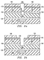
- a first etch stop layer 130 is formed over a copper layer 120 and a dielectric layer 100 as shown in Figure 2(a).
- the dielectric layer 100 is formed over a silicon substrate which contains one or more electronic devices such as transistors, diodes, etc. These electronic devices will typically be part on an integrated circuit.
- the dielectric layer 100 may formed over various portions of an integrated circuit.
- the copper layer 120 represents a portion of the copper interconnect of the integrated circuit.
- the first etch stop layer 130 may comprise silicon nitride (SiN), silicon carbide (SiC), or any suitable material.
- a first dielectric film 140 is formed over the etch stop layer 130.
- this first dielectric layer 140 comprises florosilicate glass (FSG). Any suitable dielectric material may be used to form the first dielectric layer 140.
- a second etch stop layer 150 may or may not be formed.
- This second etch stop layer 150 comprises a material selected from the group consisting of silicon nitride (SiN), silicon carbide (SiC), or any combination of layers of these or other suitable materials.
- a second dielectric layer is formed. In an embodiment of the instant invention this second etch stop layer comprises FSG, OSG or any suitable dielectric material.
- a layer of anti-reflective coating (ARC) 170 is formed as shown in Figure 2(a). In an embodiment of the instant invention this ARC layer 170 comprises silicon oxynitride. An important property of the ARC layer 170 is that no light be reflected during the photolithographic process.
- Such an ARC film can be formed using silicon oxynitride with the following atomic percentages, silicon (30% - 55%), oxygen (20% - 50%), nitrogen (2% - 17%), and hydrogen (7% - 35%).
- a photoresist layer is formed and patterned 180.
- the ARC layer 170, the second dielectric layer 160 and the second etch stop layer 150 are etched using a multi-step etch process to form a first trench 185 as illustrated in Figure 2(a).
- the silicon oxynitride layer can be etched using a CF 4 based plasma etch process.
- a 300A to 2000A silicon oxynitride film can be etched using CF 4 with flow rates of 50sccm - 120sccm, oxygen with flow rates of 1sccm - 9sccm, argon with flow rates of 200sccm - 500sccm, and power of about 1000W to 2000W.
- One advantage of using the silicon oxynitride film is that thinner layers of photoresist (i.e. less than 3000A) can be used. This leads to improved resolution over the thicker resist films necessary in current processes.
- an argon (200sccm - 400sccm), CH 2 F 2 (10sccm - 35sccm), and oxygen (9sccm - 34sccm) based plasma etch process can be used with power levels of approximately 1000W.
- a C 5 F 8 (5sccm - 13sccm), argon (300sccm - 650sccm), and oxygen (4sccm - 13sccm) etch process with a power level of approximately 1500W can be used.
- the depth of the first trench 187 is variable.
- the embodiment represented in Figure 2(a) shows the bottom surface of the trench below the second etch stop layer. In general the required depth of the first trench depends on the thickness of the dielectric layers 140 and 160 and the required depth of the second trench.
- the remaining photoresist film 180 is removed and another patterned photoresist film is formed 190 which will be used to define the width of the second trench. This is illustrated in Figure 2(b).
- the photoresist film as an etch mask, the exposed regions of the ARC layer 170 is etched.
- the layer can be etched using a CF 4 based plasma etch process.
- a 300A to 2000A silicon oxynitride film can be etched using CF 4 with flow rates of 50sccm - 120sccm, oxygen with flow rates of 1sccm - 9sccm, argon with flow rates of 200sccm - 500sccm, and power of about 1000W to 2000W.
- the ARC layer will serve as a hardmask.
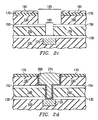
- Dielectric layers 160 and 140 are then etched simultaneously with a second trench 195 being formed in the second dielectric layer 160 and the first trench 185 etched in the first dielectric layer 140 as shown in Figure 2(c). The etching of the second trench 195 will stop on the second etch stop layer 150 (if present), and the etching of the first trench 185 in the first dielectric layer 140 will stop on the first etch stop layer 130.
- the etching of the first trench 185 is completed in the first dielectric layer.
- the first etch stop layer 130 beneath the first dielectric layer 140 is therefore not exposed to the entire second trench etching processes. This eliminates the need for the BARC protective layer currently used in the art.
- the exposed region of the first etch stop layer 130 is removed and a liner film 200 is formed as shown in Figure 2(d).
- the formation of the liner film is followed by a copper deposition and chemical mechanical polishing process which results in the copper layer 210 shown in Figure 2(d).
- the copper layer 210 is formed by first forming a thick layer of copper followed CMP processes to remove the excess copper.
Landscapes
- Internal Circuitry In Semiconductor Integrated Circuit Devices (AREA)
Abstract
Description
- The invention is generally related to the field of semiconductor devices and fabrication and more specifically to a method for forming a dual damascene structure.
- To increase the operating speed, high performance integrated circuits use copper interconnect technology along with low dielectric constant dielectrics. Currently the dual damascene method is the most widely used method for forming copper interconnects. A typical dual damascene process is illustrated in Figures 1(a) - 1(c). As shown in Figure 1(a), a first etch stop layer is formed over a
dielectric layer 10 and acopper line 20. A firstdielectric layer 40, a secondetch stop layer 50, and a seconddielectric layer 55 are formed over the first etch stop layer. A patterned layer of photoresist is then formed and used to pattern the etching of thefirst trench 57. Following the etching of thefirst trench 57, a backside anti-reflective coating (BARC)layer 60 is formed. During the formation of the BARClayer 60,additional BARC material 65 is formed in thetrench 57. Theadditional BARC material 65 is necessary to protect the bottom surface of the trench during the etching of thesecond trench 58. This is illustrated in Figure 1(b). A portion of theadditional BARC 65 is removed during the etching process. Following the etching of thesecond trench 58, trench liner material is formed 80 andcopper 90 is used to fill both trenches as illustrated in Figure 1(c). - There are a number of important issues concerning the use of the additional BARC 65 to mask the trench. Some of the more important of these are non-uniformity in dense and isolated structures, punching through the first
etch stop layer 30 during the etching process, defects caused by the BRAC material etc. These is therefore a need for an improved process that overcomes the issues associated with the use of the BARCtrench masking material 65. - The present invention describes a process for forming dual damascene structures. In particular, a first dielectric layer is formed over a silicon substrate containing one or more electronic devices. A first etch stop layer is then formed over this first dielectric layer and a second dielectric layer is then formed over the first etch stop layer. A silicon oxynitride anti-reflective coating layer is then formed over the second dielectric layer and a first trench is etched to a first depth in the second dielectric layer and the first dielectric layer. A second trench is etched in the second dielectric layer while simultaneously etching the first trench in the first dielectric layer.
- In the drawings:
- FIGURES 1(a) - 1(c) are cross-sectional diagrams illustrating the prior art.
- FIGURES 2(a) - 2(d) are cross-sectional diagrams illustrating an embodiment of the instant invention.
- The invention will now be described with reference to Figures 2(a) - 2(d). It will be apparent to those of ordinary skill in the art that the benefits of the invention can be applied to other structures where a dual damascene process is utilized.
- The requirement of higher clock rates has lead to the use of copper to form the metal interconnect lines in integrated circuits. In addition to the use of copper, dielectric layers such as organosilicate glass (OSG) (dielectric constant ∼2.6) and florosilicate glass (FSG) are currently being used to take advantage of the lower dielectric constant of such materials compared to silicon dioxide. In an embodiment of the instant invention, a first
etch stop layer 130 is formed over acopper layer 120 and adielectric layer 100 as shown in Figure 2(a). Thedielectric layer 100 is formed over a silicon substrate which contains one or more electronic devices such as transistors, diodes, etc. These electronic devices will typically be part on an integrated circuit. Thedielectric layer 100 may formed over various portions of an integrated circuit. Thecopper layer 120 represents a portion of the copper interconnect of the integrated circuit. The firstetch stop layer 130 may comprise silicon nitride (SiN), silicon carbide (SiC), or any suitable material. Following formation of the firstetch stop layer 130, a firstdielectric film 140 is formed over theetch stop layer 130. In an embodiment of the instant invention this firstdielectric layer 140 comprises florosilicate glass (FSG). Any suitable dielectric material may be used to form the firstdielectric layer 140. Following the formation of the firstdielectric layer 140, a secondetch stop layer 150 may or may not be formed. This secondetch stop layer 150 comprises a material selected from the group consisting of silicon nitride (SiN), silicon carbide (SiC), or any combination of layers of these or other suitable materials. Following the formation of the secondetch stop layer 150, a second dielectric layer is formed. In an embodiment of the instant invention this second etch stop layer comprises FSG, OSG or any suitable dielectric material. Following the formation of the seconddielectric layer 160, a layer of anti-reflective coating (ARC) 170 is formed as shown in Figure 2(a). In an embodiment of the instant invention thisARC layer 170 comprises silicon oxynitride. An important property of theARC layer 170 is that no light be reflected during the photolithographic process. Such an ARC film can be formed using silicon oxynitride with the following atomic percentages, silicon (30% - 55%), oxygen (20% - 50%), nitrogen (2% - 17%), and hydrogen (7% - 35%). Following the formation of theARC layer 170, a photoresist layer is formed and patterned 180. TheARC layer 170, the seconddielectric layer 160 and the secondetch stop layer 150 are etched using a multi-step etch process to form afirst trench 185 as illustrated in Figure 2(a). In an embodiment of the instant invention the silicon oxynitride layer can be etched using a CF4 based plasma etch process. In particular a 300A to 2000A silicon oxynitride film can be etched using CF4 with flow rates of 50sccm - 120sccm, oxygen with flow rates of 1sccm - 9sccm, argon with flow rates of 200sccm - 500sccm, and power of about 1000W to 2000W. One advantage of using the silicon oxynitride film is that thinner layers of photoresist (i.e. less than 3000A) can be used. This leads to improved resolution over the thicker resist films necessary in current processes. For cases where FSG is used to form the seconddielectric layer 160, an argon (200sccm - 400sccm), CH2F2 (10sccm - 35sccm), and oxygen (9sccm - 34sccm) based plasma etch process can be used with power levels of approximately 1000W. Finally to etch through the secondetch stop layer 150, a C5F8 (5sccm - 13sccm), argon (300sccm - 650sccm), and oxygen (4sccm - 13sccm) etch process with a power level of approximately 1500W can be used. The depth of thefirst trench 187 is variable. The embodiment represented in Figure 2(a) shows the bottom surface of the trench below the second etch stop layer. In general the required depth of the first trench depends on the thickness of thedielectric layers - Following the formation of the
first trench 185, the remainingphotoresist film 180 is removed and another patterned photoresist film is formed 190 which will be used to define the width of the second trench. This is illustrated in Figure 2(b). Using the photoresist film as an etch mask, the exposed regions of theARC layer 170 is etched. For the case where a silicon oxynitride ARC layer is used the layer can be etched using a CF4 based plasma etch process. In particular a 300A to 2000A silicon oxynitride film can be etched using CF4 with flow rates of 50sccm - 120sccm, oxygen with flow rates of 1sccm - 9sccm, argon with flow rates of 200sccm - 500sccm, and power of about 1000W to 2000W. During the subsequent etching of thedielectric layers Dielectric layers second trench 195 being formed in thesecond dielectric layer 160 and thefirst trench 185 etched in thefirst dielectric layer 140 as shown in Figure 2(c). The etching of thesecond trench 195 will stop on the second etch stop layer 150 (if present), and the etching of thefirst trench 185 in thefirst dielectric layer 140 will stop on the firstetch stop layer 130. - During the formation of the
second trench 195 in thesecond dielectric layer 160, the etching of thefirst trench 185 is completed in the first dielectric layer. The firstetch stop layer 130 beneath thefirst dielectric layer 140 is therefore not exposed to the entire second trench etching processes. This eliminates the need for the BARC protective layer currently used in the art. - Following the formation of both trenches (185 and 195) the exposed region of the first
etch stop layer 130 is removed and aliner film 200 is formed as shown in Figure 2(d). The formation of the liner film is followed by a copper deposition and chemical mechanical polishing process which results in thecopper layer 210 shown in Figure 2(d). Typically thecopper layer 210 is formed by first forming a thick layer of copper followed CMP processes to remove the excess copper. - While this invention has been described with reference to illustrative embodiments, this description is not intended to be construed in a limiting sense. Various modifications and combinations of the illustrative embodiments, as well as other embodiments of the invention will be apparent to persons skilled in the art upon reference to the description. It is therefore intended that the appended claims encompass any such modifications or embodiments.
Claims (10)
- A method for forming a dual damascene structure, comprising:providing a silicon substrate containing one or more electronic devices;forming a first dielectric layer of a first thickness over said silicon substrate;forming a first etch stop layer over said first dielectric layer;forming a second dielectric layer of a second thickness over said first dielectric layer;forming an anti-reflective coating layer over said second dielectric layer;etching a first trench to a first depth in said second dielectric layer wherein the first depth is greater than the thickness of said second dielectric layer; andsimultaneously etching a second trench to a second depth in said second dielectric layer and etching said first trench in said first dielectric layer wherein the second depth is approximately equal to the second thickness and the first depth is approximately equal to the first thickness.
- The method of claim 1 wherein said anti-reflective coating layer comprises silicon oxynitride.
- The method of claim 1 or claim 2, wherein first and second etch stop layers are formed with material selected from the group consisting of silicon carbide and silicon nitride.
- The method of any preceding claim, wherein said first dielectric layer is FSG.
- The method of any preceding claim, wherein said second dielectric layer is FSG.
- The method of any preceding claim, further comprising:forming a liner film in said first trench and said second trench; andforming a contiguous copper layer in said first trench and said second trench.
- A method for forming a copper filled dual damascene structure, comprising:providing a silicon substrate containing one or more electronic devices;forming a first dielectric layer of a first thickness over said silicon substrate;forming a first etch stop layer over said first dielectric layer;forming a second dielectric layer of a second thickness over said first dielectric layer;forming a silicon oxynitride anti-reflective coating layer over said second dielectric layer;etching a first trench to a first depth in said second dielectric layer and said first dielectric layer wherein the first depth is greater than the thickness of said second dielectric layer; andsimultaneously etching a second trench to a second depth in said second dielectric layer and etching said first trench in said first dielectric layer wherein the second depth is approximately equal to the second thickness and the first depth is approximately equal to the first thickness.
- The method of claim 7 wherein said silicon nitride anti-reflective coating layer comprises 30 to 50 atomic percent of silicon, 20 to 50 atomic percent of oxygen, 2 to 17 atomic percent of nitrogen, and 7 to 35 atomic percent of hydrogen.
- The method of claim 7 or claim 8, wherein first and second etch stop layers are formed with material selected from the group consisting of silicon carbide and silicon nitride.
- The method of claim 7, claim 8 or claim 9, wherein said first dielectric layer is FSG.
Applications Claiming Priority (2)
| Application Number | Priority Date | Filing Date | Title |
|---|---|---|---|
| US901331 | 2001-07-09 | ||
| US09/901,331 US6605540B2 (en) | 2001-07-09 | 2001-07-09 | Process for forming a dual damascene structure |
Publications (2)
| Publication Number | Publication Date |
|---|---|
| EP1280197A1 true EP1280197A1 (en) | 2003-01-29 |
| EP1280197B1 EP1280197B1 (en) | 2010-02-17 |
Family
ID=25413959
Family Applications (1)
| Application Number | Title | Priority Date | Filing Date |
|---|---|---|---|
| EP02100794A Expired - Lifetime EP1280197B1 (en) | 2001-07-09 | 2002-07-09 | Process for forming a dual damascene structure |
Country Status (4)
| Country | Link |
|---|---|
| US (2) | US6605540B2 (en) |
| EP (1) | EP1280197B1 (en) |
| JP (1) | JP2003100864A (en) |
| DE (1) | DE60235338D1 (en) |
Families Citing this family (29)
| Publication number | Priority date | Publication date | Assignee | Title |
|---|---|---|---|---|
| WO2002017374A1 (en) * | 2000-08-18 | 2002-02-28 | Tokyo Electron Limited | Low-dielectric silicon nitride film and method of forming the same, semiconductor device and fabrication process thereof |
| US6605540B2 (en) * | 2001-07-09 | 2003-08-12 | Texas Instruments Incorporated | Process for forming a dual damascene structure |
| US7183201B2 (en) * | 2001-07-23 | 2007-02-27 | Applied Materials, Inc. | Selective etching of organosilicate films over silicon oxide stop etch layers |
| JP2003209166A (en) * | 2002-01-17 | 2003-07-25 | Seiko Epson Corp | Semiconductor device and manufacturing method thereof |
| DE10219398B4 (en) * | 2002-04-30 | 2007-06-06 | Infineon Technologies Ag | Manufacturing method for a trench arrangement with trenches of different depths in a semiconductor substrate |
| JP4571785B2 (en) | 2003-05-30 | 2010-10-27 | ルネサスエレクトロニクス株式会社 | Manufacturing method of semiconductor device |
| US20050059233A1 (en) * | 2003-09-12 | 2005-03-17 | Ming-Tsong Wang | Process for forming metal damascene structure to prevent dielectric layer peeling |
| CN1299348C (en) * | 2003-09-28 | 2007-02-07 | 中芯国际集成电路制造(上海)有限公司 | Forming method of oblique inlaid inner connection structure of integrated circuit |
| US6949460B2 (en) * | 2003-11-12 | 2005-09-27 | Lam Research Corporation | Line edge roughness reduction for trench etch |
| KR101016340B1 (en) | 2003-12-15 | 2011-02-22 | 매그나칩 반도체 유한회사 | Inductor manufacturing method of high frequency semiconductor device |
| US7504727B2 (en) * | 2004-05-14 | 2009-03-17 | International Business Machines Corporation | Semiconductor interconnect structure utilizing a porous dielectric material as an etch stop layer between adjacent non-porous dielectric materials |
| US7235489B2 (en) * | 2004-05-21 | 2007-06-26 | Agere Systems Inc. | Device and method to eliminate shorting induced by via to metal misalignment |
| US7067435B2 (en) * | 2004-09-29 | 2006-06-27 | Texas Instruments Incorporated | Method for etch-stop layer etching during damascene dielectric etching with low polymerization |
| KR100641485B1 (en) * | 2004-12-28 | 2006-11-01 | 동부일렉트로닉스 주식회사 | Semiconductor device manufacturing method |
| JP4550678B2 (en) * | 2005-07-07 | 2010-09-22 | 株式会社東芝 | Semiconductor device |
| US7394154B2 (en) * | 2005-09-13 | 2008-07-01 | International Business Machines Corporation | Embedded barrier for dielectric encapsulation |
| US7416953B2 (en) * | 2005-10-31 | 2008-08-26 | Taiwan Semiconductor Manufacturing Co., Ltd. | Vertical MIM capacitors and method of fabricating the same |
| US20070290347A1 (en) * | 2006-06-19 | 2007-12-20 | Texas Instruments Incorporated | Semiconductive device having resist poison aluminum oxide barrier and method of manufacture |
| JP5128851B2 (en) * | 2007-05-30 | 2013-01-23 | ルネサスエレクトロニクス株式会社 | Semiconductor device and manufacturing method thereof |
| US7994639B2 (en) * | 2007-07-31 | 2011-08-09 | International Business Machines Corporation | Microelectronic structure including dual damascene structure and high contrast alignment mark |
| DE102008063430B4 (en) * | 2008-12-31 | 2016-11-24 | Advanced Micro Devices, Inc. | Method for producing a metallization system of a semiconductor device with additionally tapered junction contacts |
| CN101905854B (en) * | 2009-06-04 | 2012-08-22 | 台湾积体电路制造股份有限公司 | Electronic components and their production methods, electronic systems |
| US10586689B2 (en) * | 2009-07-31 | 2020-03-10 | Guardian Europe S.A.R.L. | Sputtering apparatus including cathode with rotatable targets, and related methods |
| US8227339B2 (en) | 2009-11-02 | 2012-07-24 | International Business Machines Corporation | Creation of vias and trenches with different depths |
| US20130288474A1 (en) * | 2012-04-27 | 2013-10-31 | Applied Materials, Inc. | Methods for fabricating dual damascene interconnect structures |
| US8986921B2 (en) * | 2013-01-15 | 2015-03-24 | International Business Machines Corporation | Lithographic material stack including a metal-compound hard mask |
| US9390964B2 (en) | 2013-03-15 | 2016-07-12 | Applied Materials, Inc. | Methods for fabricating dual damascene structures in low temperature dielectric materials |
| US9917027B2 (en) * | 2015-12-30 | 2018-03-13 | Globalfoundries Singapore Pte. Ltd. | Integrated circuits with aluminum via structures and methods for fabricating the same |
| KR102285787B1 (en) | 2017-03-03 | 2021-08-04 | 삼성전자 주식회사 | three dimensional semiconductor device |
Citations (4)
| Publication number | Priority date | Publication date | Assignee | Title |
|---|---|---|---|---|
| EP0975010A1 (en) * | 1998-07-22 | 2000-01-26 | Siemens Aktiengesellschaft | Prevention of photoresist poisoning from dielectric antireflective coating in semiconductor fabrication |
| US6060380A (en) | 1998-11-06 | 2000-05-09 | Advanced Micro Devices, Inc. | Antireflective siliconoxynitride hardmask layer used during etching processes in integrated circuit fabrication |
| WO2001015219A2 (en) * | 1999-08-25 | 2001-03-01 | Infineon Technologies Ag | Method for producing an integrated circuit having at least one metalicized surface |
| US6235653B1 (en) * | 1999-06-04 | 2001-05-22 | Taiwan Semiconductor Manufacturing Company | Ar-based si-rich oxynitride film for dual damascene and/or contact etch stop layer |
Family Cites Families (15)
| Publication number | Priority date | Publication date | Assignee | Title |
|---|---|---|---|---|
| US6303523B2 (en) * | 1998-02-11 | 2001-10-16 | Applied Materials, Inc. | Plasma processes for depositing low dielectric constant films |
| US6380096B2 (en) * | 1998-07-09 | 2002-04-30 | Applied Materials, Inc. | In-situ integrated oxide etch process particularly useful for copper dual damascene |
| KR20000013397A (en) * | 1998-08-07 | 2000-03-06 | 윤종용 | Manufacturing method of trench isolation |
| KR100300628B1 (en) * | 1999-02-08 | 2001-09-26 | 윤종용 | Semiconductor device having silicon oxynitride passivation layer and method for manufacturing the same |
| US6228760B1 (en) * | 1999-03-08 | 2001-05-08 | Taiwan Semiconductor Manufacturing Company | Use of PE-SiON or PE-OXIDE for contact or via photo and for defect reduction with oxide and W chemical-mechanical polish |
| US6326301B1 (en) * | 1999-07-13 | 2001-12-04 | Motorola, Inc. | Method for forming a dual inlaid copper interconnect structure |
| US6391761B1 (en) * | 1999-09-20 | 2002-05-21 | Taiwan Semiconductor Manufacturing Company | Method to form dual damascene structures using a linear passivation |
| US6429119B1 (en) * | 1999-09-27 | 2002-08-06 | Taiwan Semiconductor Manufacturing Company | Dual damascene process to reduce etch barrier thickness |
| US6222241B1 (en) * | 1999-10-29 | 2001-04-24 | Advanced Micro Devices, Inc. | Method and system for reducing ARC layer removal by providing a capping layer for the ARC layer |
| US6329281B1 (en) * | 1999-12-03 | 2001-12-11 | Agere Systems Guardian Corp. | Methods for fabricating a multilevel interconnection for an integrated circuit device utilizing a selective overlayer |
| US6342448B1 (en) * | 2000-05-31 | 2002-01-29 | Taiwan Semiconductor Manufacturing Company | Method of fabricating barrier adhesion to low-k dielectric layers in a copper damascene process |
| US6410437B1 (en) * | 2000-06-30 | 2002-06-25 | Lam Research Corporation | Method for etching dual damascene structures in organosilicate glass |
| US6475929B1 (en) * | 2001-02-01 | 2002-11-05 | Advanced Micro Devices, Inc. | Method of manufacturing a semiconductor structure with treatment to sacrificial stop layer producing diffusion to an adjacent low-k dielectric layer lowering the constant |
| US6511922B2 (en) * | 2001-03-26 | 2003-01-28 | Applied Materials, Inc. | Methods and apparatus for producing stable low k FSG film for HDP-CVD |
| US6605540B2 (en) * | 2001-07-09 | 2003-08-12 | Texas Instruments Incorporated | Process for forming a dual damascene structure |
-
2001
- 2001-07-09 US US09/901,331 patent/US6605540B2/en not_active Expired - Lifetime
-
2002
- 2002-07-09 DE DE60235338T patent/DE60235338D1/de not_active Expired - Lifetime
- 2002-07-09 JP JP2002199839A patent/JP2003100864A/en active Pending
- 2002-07-09 EP EP02100794A patent/EP1280197B1/en not_active Expired - Lifetime
-
2003
- 2003-06-27 US US10/608,286 patent/US7112532B2/en not_active Expired - Lifetime
Patent Citations (4)
| Publication number | Priority date | Publication date | Assignee | Title |
|---|---|---|---|---|
| EP0975010A1 (en) * | 1998-07-22 | 2000-01-26 | Siemens Aktiengesellschaft | Prevention of photoresist poisoning from dielectric antireflective coating in semiconductor fabrication |
| US6060380A (en) | 1998-11-06 | 2000-05-09 | Advanced Micro Devices, Inc. | Antireflective siliconoxynitride hardmask layer used during etching processes in integrated circuit fabrication |
| US6235653B1 (en) * | 1999-06-04 | 2001-05-22 | Taiwan Semiconductor Manufacturing Company | Ar-based si-rich oxynitride film for dual damascene and/or contact etch stop layer |
| WO2001015219A2 (en) * | 1999-08-25 | 2001-03-01 | Infineon Technologies Ag | Method for producing an integrated circuit having at least one metalicized surface |
Also Published As
| Publication number | Publication date |
|---|---|
| EP1280197B1 (en) | 2010-02-17 |
| US7112532B2 (en) | 2006-09-26 |
| DE60235338D1 (en) | 2010-04-01 |
| US6605540B2 (en) | 2003-08-12 |
| US20030008512A1 (en) | 2003-01-09 |
| US20040092113A1 (en) | 2004-05-13 |
| JP2003100864A (en) | 2003-04-04 |
Similar Documents
| Publication | Publication Date | Title |
|---|---|---|
| US6605540B2 (en) | Process for forming a dual damascene structure | |
| KR100531561B1 (en) | Copper interconnect structure and method of formation | |
| EP1276147A2 (en) | Dual hardmask process for the formation of copper/low-K interconnects | |
| US6184128B1 (en) | Method using a thin resist mask for dual damascene stop layer etch | |
| US6228760B1 (en) | Use of PE-SiON or PE-OXIDE for contact or via photo and for defect reduction with oxide and W chemical-mechanical polish | |
| US6605545B2 (en) | Method for forming hybrid low-K film stack to avoid thermal stress effect | |
| US6458705B1 (en) | Method for forming via-first dual damascene interconnect structure | |
| US6410426B1 (en) | Damascene cap layer process for integrated circuit interconnects | |
| US6060380A (en) | Antireflective siliconoxynitride hardmask layer used during etching processes in integrated circuit fabrication | |
| US7285853B2 (en) | Multilayer anti-reflective coating for semiconductor lithography and the method for forming the same | |
| US7323408B2 (en) | Metal barrier cap fabrication by polymer lift-off | |
| CN100437971C (en) | Method of forming a capping layer with anti-reflection properties on a low-k dielectric | |
| US6774031B2 (en) | Method of forming dual-damascene structure | |
| US6313025B1 (en) | Process for manufacturing an integrated circuit including a dual-damascene structure and an integrated circuit | |
| JP2006128542A (en) | Manufacturing method of electronic device | |
| KR100614782B1 (en) | A process for manufacturing an integrated circuit including a dual- damascene structure and an integrated circuit | |
| US20070232048A1 (en) | Damascene interconnection having a SiCOH low k layer | |
| JP2004289155A (en) | BARC etching with highly polymerizable gas for selective etching chemistry and CD control | |
| EP1286387A9 (en) | Method to reduce photoresist contamination from silicon carbide films | |
| KR20030077455A (en) | Method for manufacturing semiconductor device using dual-damascene techniques | |
| EP1282164A2 (en) | Method to improve the adhesion of dielectric layers to copper | |
| KR20040101008A (en) | Manufacturing method for semiconductor apparatus | |
| US20030044726A1 (en) | Method for reducing light reflectance in a photolithographic process | |
| JP2005005697A (en) | Manufacturing method of semiconductor device | |
| US6057246A (en) | Method for etching a metal layer with dimensional control |
Legal Events
| Date | Code | Title | Description |
|---|---|---|---|
| PUAI | Public reference made under article 153(3) epc to a published international application that has entered the european phase |
Free format text: ORIGINAL CODE: 0009012 |
|
| AK | Designated contracting states |
Designated state(s): AT BE BG CH CY CZ DE DK EE ES FI FR GB GR IE IT LI LU MC NL PT SE SK TR |
|
| AX | Request for extension of the european patent |
Extension state: AL LT LV MK RO SI |
|
| 17P | Request for examination filed |
Effective date: 20030729 |
|
| AKX | Designation fees paid |
Designated state(s): DE FR GB |
|
| 17Q | First examination report despatched |
Effective date: 20090114 |
|
| GRAP | Despatch of communication of intention to grant a patent |
Free format text: ORIGINAL CODE: EPIDOSNIGR1 |
|
| GRAS | Grant fee paid |
Free format text: ORIGINAL CODE: EPIDOSNIGR3 |
|
| GRAA | (expected) grant |
Free format text: ORIGINAL CODE: 0009210 |
|
| AK | Designated contracting states |
Kind code of ref document: B1 Designated state(s): DE FR GB |
|
| REG | Reference to a national code |
Ref country code: GB Ref legal event code: FG4D |
|
| REF | Corresponds to: |
Ref document number: 60235338 Country of ref document: DE Date of ref document: 20100401 Kind code of ref document: P |
|
| PLBE | No opposition filed within time limit |
Free format text: ORIGINAL CODE: 0009261 |
|
| STAA | Information on the status of an ep patent application or granted ep patent |
Free format text: STATUS: NO OPPOSITION FILED WITHIN TIME LIMIT |
|
| 26N | No opposition filed |
Effective date: 20101118 |
|
| REG | Reference to a national code |
Ref country code: FR Ref legal event code: PLFP Year of fee payment: 15 |
|
| REG | Reference to a national code |
Ref country code: FR Ref legal event code: PLFP Year of fee payment: 16 |
|
| PGFP | Annual fee paid to national office [announced via postgrant information from national office to epo] |
Ref country code: FR Payment date: 20170621 Year of fee payment: 16 Ref country code: GB Payment date: 20170626 Year of fee payment: 16 |
|
| PGFP | Annual fee paid to national office [announced via postgrant information from national office to epo] |
Ref country code: DE Payment date: 20170726 Year of fee payment: 16 |
|
| REG | Reference to a national code |
Ref country code: DE Ref legal event code: R119 Ref document number: 60235338 Country of ref document: DE |
|
| GBPC | Gb: european patent ceased through non-payment of renewal fee |
Effective date: 20180709 |
|
| PG25 | Lapsed in a contracting state [announced via postgrant information from national office to epo] |
Ref country code: GB Free format text: LAPSE BECAUSE OF NON-PAYMENT OF DUE FEES Effective date: 20180709 Ref country code: DE Free format text: LAPSE BECAUSE OF NON-PAYMENT OF DUE FEES Effective date: 20190201 Ref country code: FR Free format text: LAPSE BECAUSE OF NON-PAYMENT OF DUE FEES Effective date: 20180731 |