EP1280033A1 - EMC immune low drop regulator - Google Patents
EMC immune low drop regulator Download PDFInfo
- Publication number
- EP1280033A1 EP1280033A1 EP01402035A EP01402035A EP1280033A1 EP 1280033 A1 EP1280033 A1 EP 1280033A1 EP 01402035 A EP01402035 A EP 01402035A EP 01402035 A EP01402035 A EP 01402035A EP 1280033 A1 EP1280033 A1 EP 1280033A1
- Authority
- EP
- European Patent Office
- Prior art keywords
- mosfet
- emc
- stabilising
- voltage
- circuit
- Prior art date
- Legal status (The legal status is an assumption and is not a legal conclusion. Google has not performed a legal analysis and makes no representation as to the accuracy of the status listed.)
- Granted
Links
- 230000003019 stabilising effect Effects 0.000 claims abstract description 31
- 239000000758 substrate Substances 0.000 claims abstract description 13
- 230000001105 regulatory effect Effects 0.000 claims abstract description 9
- 238000000034 method Methods 0.000 claims description 4
- 230000036039 immunity Effects 0.000 description 3
- 239000003990 capacitor Substances 0.000 description 2
- 230000003071 parasitic effect Effects 0.000 description 2
- 238000007599 discharging Methods 0.000 description 1
- 238000004870 electrical engineering Methods 0.000 description 1
- 238000001914 filtration Methods 0.000 description 1
- 239000002184 metal Substances 0.000 description 1
- 230000000087 stabilizing effect Effects 0.000 description 1
Images


Classifications
-
- G—PHYSICS
- G05—CONTROLLING; REGULATING
- G05F—SYSTEMS FOR REGULATING ELECTRIC OR MAGNETIC VARIABLES
- G05F3/00—Non-retroactive systems for regulating electric variables by using an uncontrolled element, or an uncontrolled combination of elements, such element or such combination having self-regulating properties
- G05F3/02—Regulating voltage or current
- G05F3/08—Regulating voltage or current wherein the variable is DC
- G05F3/10—Regulating voltage or current wherein the variable is DC using uncontrolled devices with non-linear characteristics
- G05F3/16—Regulating voltage or current wherein the variable is DC using uncontrolled devices with non-linear characteristics being semiconductor devices
- G05F3/20—Regulating voltage or current wherein the variable is DC using uncontrolled devices with non-linear characteristics being semiconductor devices using diode- transistor combinations
- G05F3/26—Current mirrors
- G05F3/262—Current mirrors using field-effect transistors only
Definitions
- the present invention is related to supply regulators. More particularly, the present invention is related to electromagnetic compliant supply regulators.
- EMC electromagnetic compatibility
- the present invention aims to provide EMC immunity to transconductance regulators with a p-type active component.
- the present invention is a voltage regulator circuit for providing a regulated output voltage at an output terminal, said regulator circuit comprising
- the gate of the EMC stabilising MOSFET is coupled to the gate of the follower MOSFET, and the drain of the EMC stabilizing MOSFET is coupled to the source of the follower MOSFET.
- the source of the EMC stabilising MOSFET is coupled to the drain of the follower MOSFET.
- the gate of the EMC stabilising MOSFET is kept at a predetermined voltage (V bias ). Said predetermined voltage should preferably be external and independent from the input voltage.
- the drain of the EMC stabilising MOSFET is connected to the source of the driver MOSFET.
- the voltage regulator circuit of the invention further comprises a second EMC stabilising MOSFET having its drain connected to its substrate and placed in series with the driver or follower MOSFET.
- this second EMC stabilising MOSFET is placed in series with the MOSFET of the current mirror that wasn't already stabilised by the first EMC stabilising MOSFET.
- the source of the EMC stabilising MOSFET is connected to the drain of the follower MOSFET and the source of the second EMC stabilising MOSFET is connected to the drain of the driver MOSFET, both gates of said EMC stabilising MOSFET and said second EMC stabilising MOSFET being connected.
- the gates of the EMC stabilising MOSFET and the second EMC stabilising MOSFET are kept at a predetermined voltage (V bias ), which should preferably be external and independent from the input voltage.
- Another aspect of the present invention concerns a method for improving EMC stability of an electronic circuit comprising at least one circuit MOSFET, characterised by the step of providing an EMC stabilising MOSFET placed in series with said circuit MOSFET.
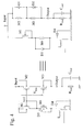
- Fig. 1 represents the basic load regulator output structure and its EMC equivalent circuit (preceded by an "equivalent sign”.
- Figs. 2 and 3 represent embodiments of the present invention and their equivalent EMC circuits.
- Fig. 4 represents a preferred embodiment of the present invention and its EMC equivalent circuit.
- the present invention comprises the use of a PMOS with its bulk or substrate connected to the drain as an EMC protection between the device to be protected and the node with the EMC disturbance. Any diode between the input supply and the regulated supply is thereby eliminated by means of an additional diode in an anti-series connection.
- the drain of the EMC protecting pMOS transistor is connected with its substrate or bulk, which in most CMOS processes concerns the n-well. This is opposite the transistors used in most active circuitry, such as for instance the current mirror circuitry of the voltage regulator, which have their sources connected to their substrate.
- the drain contact of the EMC stabilising PMOS is thus for instance connected via a metal line to the n-well contact.
- other variant methods for realising this connection can be envisaged.
- a regulated supply according to the present invention will stay regulated and constant even under strong EMC conditions on the input supply rail as will be explained in the next paragraphs.
- the EMC equivalent of this prior art topology is shown at the right hand side of Fig. 1
- an additional gate (M 3 ) is connected to net1. This can lead to stability problems. This problem can be solved by using the circuit as provided in fig. 3. On the right is provided its EMC equivalent circuit.
- V bias is an external voltage source. Such a biasing voltage source can be easily made from a current source and a resistor and will therefore not be further described.
- the current source device I control It is usually built from an n-type device and has a parasitic diode (D 4 ) to the substrate. If an additional circuit is not added, D 4 will cause a dc level shift (up) of V(netl) and as a consequence, R on of M 2 will increase and C Load will be discharged.
- D 4 parasitic diode
Landscapes
- Engineering & Computer Science (AREA)
- Microelectronics & Electronic Packaging (AREA)
- Physics & Mathematics (AREA)
- Radar, Positioning & Navigation (AREA)
- Electromagnetism (AREA)
- General Physics & Mathematics (AREA)
- Nonlinear Science (AREA)
- Automation & Control Theory (AREA)
- Control Of Electrical Variables (AREA)
- Amplifiers (AREA)
- Logic Circuits (AREA)
- Metal-Oxide And Bipolar Metal-Oxide Semiconductor Integrated Circuits (AREA)
- Semiconductor Integrated Circuits (AREA)
Abstract
- a current source (Icontrol), comprising a current source MOSFET,
- a current mirror circuit, comprising a driver MOSFET (M1) and a follower MOSFET (M2) interposed between said current source and said output terminal,
characterised in that the circuit further comprises an EMC stabilising MOSFET having its drain connected to its substrate and placed in series with any of said driver or follower MOSFETs.
Description
- The present invention is related to supply regulators. More particularly, the present invention is related to electromagnetic compliant supply regulators.
- Electrical noise has been recognised as a problem for electrical and electronic devices as from the start of electrical engineering itself. Electrical interference and the frequencies at which it occurs are growing with the rapid spread of electrical and electronic devices.
- Today, one must recognise that almost any device which operates on the principle of moving an electron from one point to another can be either a source or receiver of Electromagnetic interference (EMI).
- When two electrical or electronic devices must operate together in the same environment or in the same system, the potential for conflict between these unintended transmitters and receivers can present significant, and challenging problems. Some problems are obvious in the first prototype of a new device if it tends to 'self interfere'. This can happen when the design results in a strong emitter and a sensitive receiver in the same package.
- However, if a circuit is only a strong transmitter, or only a sensitive receiver, the potential for later problems is there, but may not be discovered until the design has left the engineering development laboratory, unless the device is tested for electromagnetic compatibility (EMC).
- Traditional transconductance regulators are not EMC safe. They can usually be considered as sensitive receivers. Electromagnetic interference will therefore usually lead to instability of the output. Traditional solutions consist of adding filters in the input line for filtering out the EMC noise on this input signal. Such filters are very expensive and require external components.
- The present invention aims to provide EMC immunity to transconductance regulators with a p-type active component.
- The present invention is a voltage regulator circuit for providing a regulated output voltage at an output terminal, said regulator circuit comprising
- a current source, comprising a current source MOSFET,
- a current mirror circuit, comprising a driver MOSFET and a follower MOSFET both having the source connected to the substrate, interposed between said current source and said output terminal,
- In an embodiment of the present invention, the gate of the EMC stabilising MOSFET is coupled to the gate of the follower MOSFET, and the drain of the EMC stabilizing MOSFET is coupled to the source of the follower MOSFET.
- In another embodiment, the source of the EMC stabilising MOSFET is coupled to the drain of the follower MOSFET. Preferably, the gate of the EMC stabilising MOSFET is kept at a predetermined voltage (Vbias). Said predetermined voltage should preferably be external and independent from the input voltage.
- In another embodiment, the drain of the EMC stabilising MOSFET is connected to the source of the driver MOSFET.
- In a preferred embodiment, the voltage regulator circuit of the invention further comprises a second EMC stabilising MOSFET having its drain connected to its substrate and placed in series with the driver or follower MOSFET. Evidently, this second EMC stabilising MOSFET is placed in series with the MOSFET of the current mirror that wasn't already stabilised by the first EMC stabilising MOSFET.
- Preferably, the source of the EMC stabilising MOSFET is connected to the drain of the follower MOSFET and the source of the second EMC stabilising MOSFET is connected to the drain of the driver MOSFET, both gates of said EMC stabilising MOSFET and said second EMC stabilising MOSFET being connected.
- Advantageously, the gates of the EMC stabilising MOSFET and the second EMC stabilising MOSFET are kept at a predetermined voltage (Vbias), which should preferably be external and independent from the input voltage.
- Another aspect of the present invention concerns a method for improving EMC stability of an electronic circuit comprising at least one circuit MOSFET, characterised by the step of providing an EMC stabilising MOSFET placed in series with said circuit MOSFET.
- Fig. 1 represents the basic load regulator output structure and its EMC equivalent circuit (preceded by an "equivalent sign".
- Figs. 2 and 3 represent embodiments of the present invention and their equivalent EMC circuits.
- Fig. 4 represents a preferred embodiment of the present invention and its EMC equivalent circuit.
- EMC immunity becomes more and more important. The solution presented in this application is simple and low-cost. The present invention comprises the use of a PMOS with its bulk or substrate connected to the drain as an EMC protection between the device to be protected and the node with the EMC disturbance. Any diode between the input supply and the regulated supply is thereby eliminated by means of an additional diode in an anti-series connection.
- In the output driver structure: one transistor (M3) is added with its substrate connected to its drain, and possibly biased by a fixed bias source (see examples 1 and 2).
- In the control structure: transistor M4, also with bulk connected to drain, and biased by the same fixed bias as M3, is used as a shield to N1 (see example 3).
- The drain of the EMC protecting pMOS transistor is connected with its substrate or bulk, which in most CMOS processes concerns the n-well. This is opposite the transistors used in most active circuitry, such as for instance the current mirror circuitry of the voltage regulator, which have their sources connected to their substrate. The drain contact of the EMC stabilising PMOS is thus for instance connected via a metal line to the n-well contact. However other variant methods for realising this connection can be envisaged.
- A regulated supply according to the present invention will stay regulated and constant even under strong EMC conditions on the input supply rail as will be explained in the next paragraphs.
- A basic LD regulator output structure with current mirror, as in the prior art, is shown in fig 1. It has no EMC immunity. Indeed, when the input voltage is lower than the output voltage, load capacitor CLoad is discharged rapidly via parasitic diode D1. This capacitor is charged only via limited current from M2 when the input voltage is higher than the output voltage. In the case of electromagnetic interference, CLoad is thus more discharged than charged and output voltage drops down, which may lead to instability problems. The EMC equivalent of this prior art topology is shown at the right hand side of Fig. 1
- The invention will now be further clarified by means of several non-limiting examples and figures.
- An improved circuit can be seen in fig.2 (left), together with its EMC equivalent circuit (right). When the input voltage is lower than the output voltage, CLoad is discharged via D1 and M3 in series; when the input voltage is higher than the output voltage, CLoad is charged via D2 and M2 in series. Due to the symmetrical structure, CLoad keeps its dc charge, making the circuit more EMC stable.
- In the embodiment of example 1 an additional gate (M3) is connected to net1. This can lead to stability problems. This problem can be solved by using the circuit as provided in fig. 3. On the right is provided its EMC equivalent circuit.
- Again, discharging of CLoad via D1 and M3 in series occurs when the input voltage is lower than the output voltage and when the input voltage is higher than the output voltage, CLoad is charged via D2 and M2 in series.
- Vbias is an external voltage source. Such a biasing voltage source can be easily made from a current source and a resistor and will therefore not be further described.
- The last problem to be avoided to make the circuit fully EMC compliant is the current source device Icontrol. It is usually built from an n-type device and has a parasitic diode (D4) to the substrate. If an additional circuit is not added, D4 will cause a dc level shift (up) of V(netl) and as a consequence, Ron of M2 will increase and CLoad will be discharged.
- To avoid this, a transistor M4 is added, as can be seen on the left in fig.4. D4 is uncoupled from net1: there is no more n-junction on net1. Even if net1 went negative relative to substrate during an EMI event, this would not influence the output voltage significantly. Also shown on fig. 4 is the EMC equivalent circuit (right).
characterised in that the circuit further comprises an EMC stabilising MOSFET having its drain connected to its substrate and placed in series with any of said driver or follower MOSFETs.
Claims (11)
- A voltage regulator circuit for providing a regulated output voltage at an output terminal, said regulator circuit comprising• a current source (Icontrol), comprising a current source MOSFET,• a current mirror circuit, comprising a driver MOSFET (M1) and a follower MOSFET (M2) both having the source connected to the substrate, interposed between said current source and said output terminal,operatively linked as to regulate an input voltage Vin to said regulated output voltage,
characterised in that the circuit further comprises an EMC stabilising MOSFET having its drain connected to its substrate and placed in series with any of said driver or follower MOSFETs. - The voltage regulator circuit as in claim 1, wherein the drain of the EMC stabilising MOSFET is coupled to the source of the follower MOSFET.
- The voltage regulator circuit as in claim 2, wherein the gate of the EMC stabilising MOSFET is coupled to the gate of the follower MOSFET.
- The voltage regulator circuit as in claim 1, wherein the source of the EMC stabilising MOSFET is coupled to the drain of the follower MOSFET.
- The voltage regulator circuit as in claim 4, wherein the gate of the EMC stabilising MOSFET is kept at a predetermined voltage (Vbias).
- The voltage regulator as in claim 5, wherein the predetermined voltage is external to and independent from the input voltage.
- Voltage regulator circuit as in claim 1, wherein the drain of the EMC stabilising MOSFET is coupled to the source of the driver MOSFET.
- Voltage regulator circuit as in claim 1, further comprising a second EMC stabilising MOSFET having its drain connected to its substrate and placed in series with any of the driver or follower MOSFET.
- The voltage regulator circuit as in claim 8, wherein the source of the EMC stabilising MOSFET is coupled to the drain of the follower MOSFET and the source of the second EMC stabilising MOSFET is connected to the drain of the driver MOSFET, both gates of said EMC stabilising MOSFET and said second EMC stabilising MOSFET being connected.
- The voltage regulator circuit as in claim 9, wherein the gate of the EMC stabilising MOSFET and the second EMC stabilising MOSFET are kept at a predetermined voltage (Vbias) which is external to and independent from the input voltage.
- A method for improving EMC stability of an electronic circuit comprising at least one circuit MOSFET, characterised by the step of providing an EMC stabilising MOSFET placed in series with and in opposite sense to said circuit MOSFET.
Priority Applications (4)
| Application Number | Priority Date | Filing Date | Title |
|---|---|---|---|
| DE60120150T DE60120150T2 (en) | 2001-07-26 | 2001-07-26 | EMC-compliant voltage regulator with low loss voltage |
| EP01402035A EP1280033B1 (en) | 2001-07-26 | 2001-07-26 | EMC immune low drop regulator |
| JP2002202234A JP2003157120A (en) | 2001-07-26 | 2002-07-11 | EMC resistant low drop regulator |
| US10/195,556 US6670842B2 (en) | 2001-07-26 | 2002-07-16 | Electromagnetic compatible regulator |
Applications Claiming Priority (1)
| Application Number | Priority Date | Filing Date | Title |
|---|---|---|---|
| EP01402035A EP1280033B1 (en) | 2001-07-26 | 2001-07-26 | EMC immune low drop regulator |
Publications (2)
| Publication Number | Publication Date |
|---|---|
| EP1280033A1 true EP1280033A1 (en) | 2003-01-29 |
| EP1280033B1 EP1280033B1 (en) | 2006-05-31 |
Family
ID=8182828
Family Applications (1)
| Application Number | Title | Priority Date | Filing Date |
|---|---|---|---|
| EP01402035A Expired - Lifetime EP1280033B1 (en) | 2001-07-26 | 2001-07-26 | EMC immune low drop regulator |
Country Status (4)
| Country | Link |
|---|---|
| US (1) | US6670842B2 (en) |
| EP (1) | EP1280033B1 (en) |
| JP (1) | JP2003157120A (en) |
| DE (1) | DE60120150T2 (en) |
Cited By (1)
| Publication number | Priority date | Publication date | Assignee | Title |
|---|---|---|---|---|
| EP2028760A1 (en) * | 2007-08-22 | 2009-02-25 | AMI Semiconductor Belgium BVBA | A low side driver |
Families Citing this family (5)
| Publication number | Priority date | Publication date | Assignee | Title |
|---|---|---|---|---|
| TW200525867A (en) * | 2004-01-21 | 2005-08-01 | Renesas Tech Corp | Voltage clamp circuit, switching power supply apparatus, semiconductor IC device, and voltage level converting circuit |
| US8253394B2 (en) | 2004-02-17 | 2012-08-28 | Hewlett-Packard Development Company, L.P. | Snubber circuit |
| US20050162870A1 (en) * | 2004-01-23 | 2005-07-28 | Hirst B. M. | Power converter |
| US8717004B2 (en) * | 2011-06-30 | 2014-05-06 | Taiwan Semiconductor Manufacturing Company, Ltd. | Circuit comprising transistors that have different threshold voltage values |
| DE102021121474A1 (en) | 2021-08-18 | 2023-02-23 | Brose Schließsysteme GmbH & Co. Kommanditgesellschaft | motor vehicle lock assembly |
Citations (2)
| Publication number | Priority date | Publication date | Assignee | Title |
|---|---|---|---|---|
| US5436552A (en) * | 1992-09-22 | 1995-07-25 | Mitsubishi Denki Kabushiki Kaisha | Clamping circuit for clamping a reference voltage at a predetermined level |
| US5510699A (en) * | 1994-05-31 | 1996-04-23 | Deutsche Itt Industries Gmbh | Voltage regulator |
Family Cites Families (4)
| Publication number | Priority date | Publication date | Assignee | Title |
|---|---|---|---|---|
| DE4400872A1 (en) * | 1994-01-14 | 1995-07-20 | Philips Patentverwaltung | Output driver circuit |
| EP0878752A1 (en) | 1997-05-12 | 1998-11-18 | EM Microelectronic-Marin SA | Voltage regulation circuit for suppressing the "latch-up" effect |
| EA200100030A1 (en) * | 1998-06-12 | 2001-06-25 | Саут Айлэнд Дискритс Лимитед | EXCITATION OF THE SHUTTER FOR POWERFUL SEMICONDUCTOR DEVICES WITH ISOLATED SHUTTER |
| DE19836577C1 (en) * | 1998-08-12 | 2000-04-20 | Siemens Ag | Power circuit with reduced interference |
-
2001
- 2001-07-26 EP EP01402035A patent/EP1280033B1/en not_active Expired - Lifetime
- 2001-07-26 DE DE60120150T patent/DE60120150T2/en not_active Expired - Lifetime
-
2002
- 2002-07-11 JP JP2002202234A patent/JP2003157120A/en not_active Withdrawn
- 2002-07-16 US US10/195,556 patent/US6670842B2/en not_active Expired - Lifetime
Patent Citations (2)
| Publication number | Priority date | Publication date | Assignee | Title |
|---|---|---|---|---|
| US5436552A (en) * | 1992-09-22 | 1995-07-25 | Mitsubishi Denki Kabushiki Kaisha | Clamping circuit for clamping a reference voltage at a predetermined level |
| US5510699A (en) * | 1994-05-31 | 1996-04-23 | Deutsche Itt Industries Gmbh | Voltage regulator |
Cited By (2)
| Publication number | Priority date | Publication date | Assignee | Title |
|---|---|---|---|---|
| EP2028760A1 (en) * | 2007-08-22 | 2009-02-25 | AMI Semiconductor Belgium BVBA | A low side driver |
| US8093924B2 (en) | 2007-08-22 | 2012-01-10 | Semiconductor Components Industries, Llc | Low side driver |
Also Published As
| Publication number | Publication date |
|---|---|
| JP2003157120A (en) | 2003-05-30 |
| DE60120150T2 (en) | 2007-05-10 |
| US6670842B2 (en) | 2003-12-30 |
| EP1280033B1 (en) | 2006-05-31 |
| DE60120150D1 (en) | 2006-07-06 |
| US20030020445A1 (en) | 2003-01-30 |
Similar Documents
| Publication | Publication Date | Title |
|---|---|---|
| US7233196B2 (en) | Bandgap reference voltage generator | |
| US20060220727A1 (en) | Electronic switch and operational method for transistor | |
| US11456743B2 (en) | Differential signal transmission circuit | |
| US6066971A (en) | Integrated circuit having buffering circuitry with slew rate control | |
| US9531372B1 (en) | Driver with transformer feedback | |
| US11290059B2 (en) | Crystal oscillator interconnect architecture with noise immunity | |
| US6670842B2 (en) | Electromagnetic compatible regulator | |
| US6281731B1 (en) | Control of hysteresis characteristic within a CMOS differential receiver | |
| US6600350B2 (en) | Power-on/off reset circuit | |
| US8810218B2 (en) | Stabilized voltage regulator | |
| US6380792B1 (en) | Semiconductor integrated circuit | |
| US7402985B2 (en) | Dual path linear voltage regulator | |
| US20050280464A1 (en) | Constant voltage outputting circuit | |
| US20260012138A1 (en) | Push-pull source follower circuit using biasing technique to program bias current and output mean voltage independently | |
| US20120193518A1 (en) | Photoreceptor circuit and photocoupler | |
| JPH0637553A (en) | Dynamic limiting circuit for amplifier | |
| JP4280672B2 (en) | Semiconductor integrated circuit | |
| US10310531B2 (en) | Current and voltage regulation method to improve electromagnetice compatibility performance | |
| US11936375B2 (en) | Buffer apparatus, chip and electronic device | |
| JPH08161066A (en) | Voltage regulator | |
| US20230161364A1 (en) | Linear regulator | |
| US20090160562A1 (en) | Oscillating device | |
| KR100846880B1 (en) | Gate driver output stage with bias circuit for high and wide operating voltage range | |
| US20090027820A1 (en) | Semiconductor Integrated Circuit Device | |
| US10719097B1 (en) | Voltage regulation circuit suitable to provide output voltage to core circuit |
Legal Events
| Date | Code | Title | Description |
|---|---|---|---|
| PUAI | Public reference made under article 153(3) epc to a published international application that has entered the european phase |
Free format text: ORIGINAL CODE: 0009012 |
|
| AK | Designated contracting states |
Designated state(s): AT BE CH CY DE DK ES FI FR GB GR IE IT LI LU MC NL PT SE TR |
|
| AX | Request for extension of the european patent |
Extension state: AL LT LV MK RO SI |
|
| RAP1 | Party data changed (applicant data changed or rights of an application transferred) |
Owner name: AMI SEMICONDUCTOR BELGIUM BVBA |
|
| 17P | Request for examination filed |
Effective date: 20030708 |
|
| 17Q | First examination report despatched |
Effective date: 20030806 |
|
| AKX | Designation fees paid |
Designated state(s): DE FR |
|
| GRAP | Despatch of communication of intention to grant a patent |
Free format text: ORIGINAL CODE: EPIDOSNIGR1 |
|
| GRAS | Grant fee paid |
Free format text: ORIGINAL CODE: EPIDOSNIGR3 |
|
| GRAA | (expected) grant |
Free format text: ORIGINAL CODE: 0009210 |
|
| AK | Designated contracting states |
Kind code of ref document: B1 Designated state(s): DE FR |
|
| REF | Corresponds to: |
Ref document number: 60120150 Country of ref document: DE Date of ref document: 20060706 Kind code of ref document: P |
|
| ET | Fr: translation filed | ||
| PLBE | No opposition filed within time limit |
Free format text: ORIGINAL CODE: 0009261 |
|
| STAA | Information on the status of an ep patent application or granted ep patent |
Free format text: STATUS: NO OPPOSITION FILED WITHIN TIME LIMIT |
|
| 26N | No opposition filed |
Effective date: 20070301 |
|
| REG | Reference to a national code |
Ref country code: DE Ref legal event code: R082 Ref document number: 60120150 Country of ref document: DE Representative=s name: BIRD, WILLIAM EDWARD, MA. CENG. MIEE, DE |
|
| REG | Reference to a national code |
Ref country code: DE Ref legal event code: R082 Ref document number: 60120150 Country of ref document: DE Representative=s name: BIRD, WILLIAM EDWARD, MA. CENG. MIEE, DE |
|
| REG | Reference to a national code |
Ref country code: DE Ref legal event code: R081 Ref document number: 60120150 Country of ref document: DE Owner name: SEMICONDUCTOR COMPONENTS INDUSTRIES, LLC, US Free format text: FORMER OWNER: ON SEMICONDUCTOR BELGIUM BVBA, OUDENAARDE, BE Effective date: 20130515 Ref country code: DE Ref legal event code: R082 Ref document number: 60120150 Country of ref document: DE Representative=s name: BIRD, WILLIAM EDWARD, MA. CENG. MIEE, DE Effective date: 20130514 Ref country code: DE Ref legal event code: R081 Ref document number: 60120150 Country of ref document: DE Owner name: SEMICONDUCTOR COMPONENTS INDUSTRIES, LLC, US Free format text: FORMER OWNER: AMI SEMICONDUCTOR BELGIUM BVBA, OUDENAARDE, BE Effective date: 20130514 Ref country code: DE Ref legal event code: R082 Ref document number: 60120150 Country of ref document: DE Representative=s name: BIRD, WILLIAM EDWARD, MA. CENG. MIEE, DE Effective date: 20130515 Ref country code: DE Ref legal event code: R081 Ref document number: 60120150 Country of ref document: DE Owner name: SEMICONDUCTOR COMPONENTS INDUSTRIES, LLC, PHOE, US Free format text: FORMER OWNER: AMI SEMICONDUCTOR BELGIUM BVBA, OUDENAARDE, BE Effective date: 20130514 Ref country code: DE Ref legal event code: R081 Ref document number: 60120150 Country of ref document: DE Owner name: SEMICONDUCTOR COMPONENTS INDUSTRIES, LLC, PHOE, US Free format text: FORMER OWNER: ON SEMICONDUCTOR BELGIUM BVBA, OUDENAARDE, BE Effective date: 20130515 |
|
| REG | Reference to a national code |
Ref country code: FR Ref legal event code: CD Owner name: SEMICONDUCTOR COMPONENTS INDUSTRIES, LLC, US Effective date: 20130617 Ref country code: FR Ref legal event code: TP Owner name: SEMICONDUCTOR COMPONENTS INDUSTRIES, LLC, US Effective date: 20130617 |
|
| REG | Reference to a national code |
Ref country code: FR Ref legal event code: PLFP Year of fee payment: 16 |
|
| PGFP | Annual fee paid to national office [announced via postgrant information from national office to epo] |
Ref country code: FR Payment date: 20160621 Year of fee payment: 16 |
|
| REG | Reference to a national code |
Ref country code: FR Ref legal event code: ST Effective date: 20180330 |
|
| PG25 | Lapsed in a contracting state [announced via postgrant information from national office to epo] |
Ref country code: FR Free format text: LAPSE BECAUSE OF NON-PAYMENT OF DUE FEES Effective date: 20170731 |
|
| PGFP | Annual fee paid to national office [announced via postgrant information from national office to epo] |
Ref country code: DE Payment date: 20200622 Year of fee payment: 20 |
|
| REG | Reference to a national code |
Ref country code: DE Ref legal event code: R071 Ref document number: 60120150 Country of ref document: DE |