EP1280032A1 - Low drop voltage regulator - Google Patents
Low drop voltage regulator Download PDFInfo
- Publication number
- EP1280032A1 EP1280032A1 EP01402036A EP01402036A EP1280032A1 EP 1280032 A1 EP1280032 A1 EP 1280032A1 EP 01402036 A EP01402036 A EP 01402036A EP 01402036 A EP01402036 A EP 01402036A EP 1280032 A1 EP1280032 A1 EP 1280032A1
- Authority
- EP
- European Patent Office
- Prior art keywords
- voltage
- transistor
- circuit
- current source
- regulator
- Prior art date
- Legal status (The legal status is an assumption and is not a legal conclusion. Google has not performed a legal analysis and makes no representation as to the accuracy of the status listed.)
- Withdrawn
Links
- 230000001105 regulatory effect Effects 0.000 claims abstract description 13
- 230000007423 decrease Effects 0.000 description 3
- 238000000034 method Methods 0.000 description 3
- 230000033228 biological regulation Effects 0.000 description 1
Images


Classifications
-
- G—PHYSICS
- G05—CONTROLLING; REGULATING
- G05F—SYSTEMS FOR REGULATING ELECTRIC OR MAGNETIC VARIABLES
- G05F1/00—Automatic systems in which deviations of an electric quantity from one or more predetermined values are detected at the output of the system and fed back to a device within the system to restore the detected quantity to its predetermined value or values, i.e. retroactive systems
- G05F1/10—Regulating voltage or current
- G05F1/46—Regulating voltage or current wherein the variable actually regulated by the final control device is DC
- G05F1/56—Regulating voltage or current wherein the variable actually regulated by the final control device is DC using semiconductor devices in series with the load as final control devices
- G05F1/575—Regulating voltage or current wherein the variable actually regulated by the final control device is DC using semiconductor devices in series with the load as final control devices characterised by the feedback circuit
Definitions
- the present invention is related to supply regulators, more particularly to voltage regulator circuits of the low drop type.
- Supply regulators are commonly used throughout electric and electronic equipment to provide a stable voltage or current supply from an input that may vary in time and over different load conditions.
- Low drop regulators are known to perform well and are in high demand due to their high stability and low energy losses.
- Current low-drop regulators (see fig. 1) have a standard basic output circuit consisting of a p-type current mirror (T 4 , T 5 ) wherein the driving circuit (T 4 ) is in saturation.
- the voltage drop across T 5 can only be reduced by having a small on-resistance R on , thus by a combination of a high V GS , and by a large W/L ratio.
- V GS very high V GS is difficult due to the quadratic I/V relationship of the current through T 4 (the gain in V GS is very small compared to the current increase that is needed). So a very large PMOS for T 5 and/or a very big current through T 4 is needed to obtain a satisfying result.
- the regulator device is a regulator transistor
- said regulator transistor has a fixed gate voltage
- said first current source is directly coupled to the gate of said follower transistor.
- the voltage regulator circuit further comprises a biasing transistor and a second current source arranged to provide the fixed gate voltage of the regulator transistor.
- the fixed gate voltage is preferably selected such that for a certain maximal current I max through the driver transistor, the driver transistor is in linear mode of operation.
- a voltage regulator circuit can further comprise an input terminal for applying a reference voltage.
- the comparator circuit is an error amplifier arranged to generate an output voltage at an output node based upon a voltage difference between said regulated output voltage and said reference voltage.
- a voltage regulator circuit has preferably said driver transistor and said follower transistor interconnected at their gate, both transistors being connected with their source to said input terminal, the output terminal being the drain of the follower transistor.
- Said first current source is preferably interposed between said output node of said error amplifier and the drain of said driver transistor.
- the current mirror circuit is of the p-type.
- Fig. 1 represents the standard basic low-drop regulator circuit from the prior art. bipolar transistors. The latter therefore requires the availability of an expensive BICMOS process.
- the present invention aims to provide a new low drop regulator which is low-cost, can be realised using CMOS processing, which is stable, modest in power consumption and which performs well.
- the present invention concerns a voltage regulator circuit for providing a regulated output voltage (V out ) at an output terminal, said regulator circuit comprising
- circuit operatively linked as to regulate an input voltage V in to said regulated output voltage by comparing said output voltage with a reference voltage and adjusting said first current source to maintain said regulated output voltage at said output terminal, characterised in that the circuit further comprises a regulator device interposed between said first current source and said driver transistor.
- Said regulator device is preferably selected from the group consisting of a regulator resistor and regulator transistor.
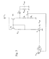
- Fig. 2 represents a preferred embodiment of the new regulator circuit according to the present invention.
- Fig. 3 represents another embodiment of the new regulator circuit according to the present invention.
- the present invention provides a low-cost pure CMOS alternative to the solutions known in the art.
- One of the prior art low-drop regulators is,by means of reference, shown in Fig. 1.
- Such a low-drop regulator provides a regulated output voltage V out at a same named output terminal, from an input voltage Vin, which is an input signal to this voltage regulator circuit at a same named input terminal, by comparing said output voltage with a reference voltage V ref , provided to the voltage regulator at a same named input terminal, and by adjusting a first current source, denoted I2, to maintain the regulated output voltage at the output terminal.
- a first current source denoted I2
- the voltage regulator circuit further comprises a current mirror circuit, comprising a driver transistor (T 4 ) and a follower transistor (T 5 ), interposed between said first current source and said output terminal.
- the main feature of the present invention consists in the addition to this prior art circuit, of a regulator device for creating a more suitable current/voltage characteristic for driving the follower transistor T 5
- This current/voltage characteristic is preferably an s-type voltage/current characteristic.
- Said regulator device can e.g. be a resistor or, more preferably, a transistor circuit.
- an additional transistor (T sol ) is added in series with T 4 , whereby this additional transistor is driven by a fixed gate voltage denoted V G .
- This gate voltage V G is such that for a certain maximum current I max through T 4 , T 4 will be driven in its linear mode of operation such that the current source I 2 will force the voltage on the gate of T 5 low.
- V GS of T 5 will thus increase substantially more compared to the saturation region. This thus allows T 5 to conduct much larger currents compared to the prior art case, such that T 5 can accordingly be made much smaller for having the same output current as in the prior art.
- the fixed V G can be obtained by a transistor T bias biased from a fixed current source I 1 .
- the stability of the loop for currents through the first current source, I 2 larger than I max is achieved mainly by following factors:
- the present invention provides a very simple solution to the low drop regulator problem: only 2 extra transistors and a current source are needed.
- a low drop regulator according to the present invention also shows smaller current consumption, as the drain current for T 4 is limited to I max .
- resistor As the regulator device. This can be seen in figure 3.
- An additional resistor (R sol ) is added between the driver transistor T 4 and the current source.
- resistor and transistor Both embodiments (resistor and transistor) will result in an s-shape characteristic of T5.
- the resistor embodiment will provide an s-shape that is not as steep as in case the transistor embodiment is used, and I max is not process independent anymore.
Landscapes
- Engineering & Computer Science (AREA)
- Physics & Mathematics (AREA)
- Electromagnetism (AREA)
- General Physics & Mathematics (AREA)
- Radar, Positioning & Navigation (AREA)
- Automation & Control Theory (AREA)
- Continuous-Control Power Sources That Use Transistors (AREA)
- Control Of Electrical Variables (AREA)
Abstract
The present invention is related to a voltage regulator circuit for providing a regulated output voltage (Vout) at an output terminal, said regulator circuit comprising
- a first current source (I2),
- a comparator circuit and
- a current mirror circuit, comprising a driver transistor (T4) and a follower transistor (T5), interposed between said first current source and said output terminal,
the circuit further comprises a regulator device interposed between said first current source and said driver transistor.
Description
- The present invention is related to supply regulators, more particularly to voltage regulator circuits of the low drop type.
- Supply regulators are commonly used throughout electric and electronic equipment to provide a stable voltage or current supply from an input that may vary in time and over different load conditions. Low drop regulators are known to perform well and are in high demand due to their high stability and low energy losses. Current low-drop regulators (see fig. 1) have a standard basic output circuit consisting of a p-type current mirror (T4, T5) wherein the driving circuit (T4) is in saturation. The voltage drop across T5 can only be reduced by having a small on-resistance Ron, thus by a combination of a high VGS, and by a large W/L ratio.
- Obtaining a very high VGS is difficult due to the quadratic I/V relationship of the current through T4 (the gain in VGS is very small compared to the current increase that is needed). So a very large PMOS for T5 and/or a very big current through T4 is needed to obtain a satisfying result.
- Another solution known in the art is described in US 6,188,211. The solution proposed in this document however is relatively complicated since it contains a lot of transistors and since it makes use of
- In case said regulator device is a regulator transistor , said regulator transistor has a fixed gate voltage, and said first current source is directly coupled to the gate of said follower transistor. Advantageously, the voltage regulator circuit further comprises a biasing transistor and a second current source arranged to provide the fixed gate voltage of the regulator transistor. The fixed gate voltage is preferably selected such that for a certain maximal current Imax through the driver transistor, the driver transistor is in linear mode of operation.
- A voltage regulator circuit according to the invention can further comprise an input terminal for applying a reference voltage. Preferably, the comparator circuit is an error amplifier arranged to generate an output voltage at an output node based upon a voltage difference between said regulated output voltage and said reference voltage.
- A voltage regulator circuit according to the present invention has preferably said driver transistor and said follower transistor interconnected at their gate, both transistors being connected with their source to said input terminal, the output terminal being the drain of the follower transistor. Said first current source is preferably interposed between said output node of said error amplifier and the drain of said driver transistor. Advantageously, the current mirror circuit is of the p-type.
- Fig. 1 represents the standard basic low-drop regulator circuit from the prior art. bipolar transistors. The latter therefore requires the availability of an expensive BICMOS process.
- The present invention aims to provide a new low drop regulator which is low-cost, can be realised using CMOS processing, which is stable, modest in power consumption and which performs well.
- The present invention concerns a voltage regulator circuit for providing a regulated output voltage (Vout) at an output terminal, said regulator circuit comprising
- a first current source,
- a comparator circuit and
- a current mirror circuit, comprising a driver transistor and a follower transistor, interposed between said first current source and said output terminal,
- operatively linked as to regulate an input voltage Vin to said regulated output voltage by comparing said output voltage with a reference voltage and adjusting said first current source to maintain said regulated output voltage at said output terminal, characterised in that the circuit further comprises a regulator device interposed between said first current source and said driver transistor.
- Said regulator device is preferably selected from the group consisting of a regulator resistor and regulator transistor.
- Fig. 2 represents a preferred embodiment of the new regulator circuit according to the present invention.
- Fig. 3 represents another embodiment of the new regulator circuit according to the present invention.
- The present invention provides a low-cost pure CMOS alternative to the solutions known in the art. One of the prior art low-drop regulators is,by means of reference, shown in Fig. 1. Such a low-drop regulator provides a regulated output voltage Vout at a same named output terminal, from an input voltage Vin, which is an input signal to this voltage regulator circuit at a same named input terminal, by comparing said output voltage with a reference voltage Vref, provided to the voltage regulator at a same named input terminal, and by adjusting a first current source, denoted I2, to maintain the regulated output voltage at the output terminal. In Fig. 1 and the other figures the operation of the first current source is schematically depicted by means of the expression gm.Vdiff, which serves as an example for this regulation, and which indicates that the current source I2 is operative based on the result of the comparator, which is denoted as circuit gm. Vdiff is thereby the input voltage to this comparator. A person skilled in the art is adapted to realise such comparators and current sources in voltage regulators and a detailed circuit for this current source and comparator is thereby not shown. The voltage regulator circuit further comprises a current mirror circuit, comprising a driver transistor (T4) and a follower transistor (T5), interposed between said first current source and said output terminal.
The main feature of the present invention consists in the addition to this prior art circuit, of a regulator device for creating a more suitable current/voltage characteristic for driving the follower transistor T5 This current/voltage characteristic is preferably an s-type voltage/current characteristic. Said regulator device can e.g. be a resistor or, more preferably, a transistor circuit. - As can be seen in figure 2, an additional transistor (Tsol) is added in series with T4, whereby this additional transistor is driven by a fixed gate voltage denoted VG. This gate voltage VG is such that for a certain maximum current Imax through T4, T4 will be driven in its linear mode of operation such that the current source I2 will force the voltage on the gate of T5 low. VGS of T5 will thus increase substantially more compared to the saturation region. This thus allows T5 to conduct much larger currents compared to the prior art case, such that T5 can accordingly be made much smaller for having the same output current as in the prior art. The fixed VG can be obtained by a transistor Tbias biased from a fixed current source I1.
- For this configuration, following equation applies :

- Imax denotes the maximum current through T4, being a design parameter for the voltage regulator.
- L(Tbias) denotes the length of transistor Tbias
- W(Tbias) denotes the width of transistor Tbias
- L(Tsol) denotes the length of transistor Tsol
- W(Tsol) denotes the width of transistor Tsol
- L(T4) denotes the length of transistor T4
- W(T4) denotes the width of transistor T4
- The stability of the loop for currents through the first current source, I2 larger than Imax, is achieved mainly by following factors:
- a) big VGS of T5 pushes T5 into linear mode and thus decreases the open loop gain
- b) the comparator being a differential transconductance stage (gm), can be easily designed with transconductance decrease for bigger input voltage Vdiff, if an unbalanced differential pair configuration is chosen, and thus with decrease of the open loop gain for I2 > Imax.
- c) for I2 = Imax, even the basic loop of Fig. 1, has a good phase margin.
- The present invention provides a very simple solution to the low drop regulator problem: only 2 extra transistors and a current source are needed.
- A low drop regulator according to the present invention also shows smaller current consumption, as the drain current for T4 is limited to Imax.
- One can also envisage using a resistor as the regulator device. This can be seen in figure 3. An additional resistor (Rsol) is added between the driver transistor T4 and the current source.
- Both embodiments (resistor and transistor) will result in an s-shape characteristic of T5. However, the resistor embodiment will provide an s-shape that is not as steep as in case the transistor embodiment is used, and Imax is not process independent anymore.
Claims (9)
- A voltage regulator circuit for providing a regulated output voltage (Vout) at an output terminal, said voltage regulator circuit comprising• a first current source (I2),• a comparator circuit and• a current mirror circuit, comprising a driver transistor (T4) and a follower transistor (T5), interposed between said first current source and said output terminal,
operatively linked as to regulate an input voltage Vin to said regulated output voltage by comparing said output voltage with a reference voltage (Vref) and adjusting said first current source to maintain said regulated output voltage at said output terminal, characterised in that
the circuit further comprises a regulator device (Tsol;Rsol)interposed between said first current source (I2) and said driver transistor (T4). - A voltage regulator circuit such as in claim 1, wherein said comparator circuit is an error amplifier arranged to generate an output voltage at an output node based upon a voltage difference between said regulated output voltage and said reference voltage.
- A voltage regulator circuit such as in claim 1 or 2, wherein said driver transistor (T4) and said follower transistor (T5) are interconnected at their gate, both transistors being connected with their source to said input terminal, the output terminal being the drain of the follower transistor.
- A voltage regulator circuit such as in any of the claims 1 to 3, wherein said first current source is interposed between said output node of said error amplifier and the drain of said driver transistor (T4).
- A voltage regulator circuit of any of the claims 1 to 4, characterised in that the current mirror circuit is of the p-type.
- A voltage regulator circuit such as in any of the claims 1 to 5, wherein said regulator device is a regulator resistor (Rsol).
- A voltage regulator circuit such as in any of the claims 1 to 5, wherein said regulator device is a regulator transistor (Tsol) having a fixed gate voltage (VG), and whereby said first current source is coupled with the gate of said follower transistor.
- The voltage regulator circuit of claim 7, characterised in that it further comprises a biasing transistor (Tbias) and a second current source (I1) arranged to provide the fixed gate voltage of the regulator transistor (Tsol).
- The voltage regulator circuit of claim 7 or 8, characterised in that the fixed gate voltage is selected such that for a certain maximal current Imax through the driver transistor (T4), the driver transistor (T4) is in linear mode of operation.
Priority Applications (3)
| Application Number | Priority Date | Filing Date | Title |
|---|---|---|---|
| EP01402036A EP1280032A1 (en) | 2001-07-26 | 2001-07-26 | Low drop voltage regulator |
| JP2002202235A JP2003099135A (en) | 2001-07-26 | 2002-07-11 | Low drop voltage regulator |
| US10/195,555 US20030020444A1 (en) | 2001-07-26 | 2002-07-16 | Low drop voltage regulator |
Applications Claiming Priority (1)
| Application Number | Priority Date | Filing Date | Title |
|---|---|---|---|
| EP01402036A EP1280032A1 (en) | 2001-07-26 | 2001-07-26 | Low drop voltage regulator |
Publications (1)
| Publication Number | Publication Date |
|---|---|
| EP1280032A1 true EP1280032A1 (en) | 2003-01-29 |
Family
ID=8182829
Family Applications (1)
| Application Number | Title | Priority Date | Filing Date |
|---|---|---|---|
| EP01402036A Withdrawn EP1280032A1 (en) | 2001-07-26 | 2001-07-26 | Low drop voltage regulator |
Country Status (3)
| Country | Link |
|---|---|
| US (1) | US20030020444A1 (en) |
| EP (1) | EP1280032A1 (en) |
| JP (1) | JP2003099135A (en) |
Cited By (3)
| Publication number | Priority date | Publication date | Assignee | Title |
|---|---|---|---|---|
| EP1658544A4 (en) * | 2003-08-29 | 2006-11-15 | Ricoh Kk | A constant-voltage circuit |
| WO2007020293A1 (en) * | 2005-08-18 | 2007-02-22 | Texas Instruments Deutschland Gmbh | Voltage regulator with low dropout voltage |
| CN103823499A (en) * | 2014-03-03 | 2014-05-28 | 西安华芯半导体有限公司 | Device for automatically adjusting output voltage of linear voltage regulator along with temperature |
Families Citing this family (8)
| Publication number | Priority date | Publication date | Assignee | Title |
|---|---|---|---|---|
| EP1439444A1 (en) * | 2003-01-16 | 2004-07-21 | Dialog Semiconductor GmbH | Low drop out voltage regulator having a cascode structure |
| US6867640B2 (en) * | 2003-07-01 | 2005-03-15 | Ami Semiconductor, Inc. | Double-sided extended drain field effect transistor, and integrated overvoltage and reverse voltage protection circuit that uses the same |
| WO2006067890A1 (en) * | 2004-12-22 | 2006-06-29 | Matsushita Electric Industrial Co., Ltd. | Optical transmitter circuit |
| US7382180B2 (en) * | 2006-04-19 | 2008-06-03 | Ememory Technology Inc. | Reference voltage source and current source circuits |
| TWI317056B (en) * | 2006-08-01 | 2009-11-11 | Novatek Microelectronics Corp | Voltage regulator |
| DE102008011603B4 (en) * | 2008-02-28 | 2009-12-31 | Semikron Elektronik Gmbh & Co. Kg | Circuit and method for signal voltage transmission within a driver of a power semiconductor switch |
| CN114564068B (en) * | 2022-03-02 | 2023-07-14 | 重庆吉芯科技有限公司 | Adaptive current generation circuit and method applied to high-speed ADC input buffer |
| JPWO2024018815A1 (en) * | 2022-07-22 | 2024-01-25 |
Citations (3)
| Publication number | Priority date | Publication date | Assignee | Title |
|---|---|---|---|---|
| EP0735452A2 (en) * | 1995-03-28 | 1996-10-02 | STMicroelectronics, Inc. | Current-limit circuit |
| EP0851332A2 (en) * | 1996-12-19 | 1998-07-01 | Texas Instruments Incorporated | A voltage regulator |
| US6188211B1 (en) * | 1998-05-13 | 2001-02-13 | Texas Instruments Incorporated | Current-efficient low-drop-out voltage regulator with improved load regulation and frequency response |
Family Cites Families (12)
| Publication number | Priority date | Publication date | Assignee | Title |
|---|---|---|---|---|
| US4808907A (en) * | 1988-05-17 | 1989-02-28 | Motorola, Inc. | Current regulator and method |
| US5646518A (en) * | 1994-11-18 | 1997-07-08 | Lucent Technologies Inc. | PTAT current source |
| US5850139A (en) * | 1997-02-28 | 1998-12-15 | Stmicroelectronics, Inc. | Load pole stabilized voltage regulator circuit |
| JP3323119B2 (en) * | 1997-11-28 | 2002-09-09 | 株式会社東芝 | Semiconductor integrated circuit device |
| US6285246B1 (en) * | 1998-09-15 | 2001-09-04 | California Micro Devices, Inc. | Low drop-out regulator capable of functioning in linear and saturated regions of output driver |
| US6087820A (en) * | 1999-03-09 | 2000-07-11 | Siemens Aktiengesellschaft | Current source |
| WO2001046768A1 (en) * | 1999-12-21 | 2001-06-28 | Koninklijke Philips Electronics N.V. | Voltage regulator provided with a current limiter |
| JP4697997B2 (en) * | 2000-04-13 | 2011-06-08 | エルピーダメモリ株式会社 | Internal voltage generation circuit |
| US6343024B1 (en) * | 2000-06-20 | 2002-01-29 | Stmicroelectronics, Inc. | Self-adjustable impedance line driver with hybrid |
| US6359427B1 (en) * | 2000-08-04 | 2002-03-19 | Maxim Integrated Products, Inc. | Linear regulators with low dropout and high line regulation |
| US6448750B1 (en) * | 2001-04-05 | 2002-09-10 | Saifun Semiconductor Ltd. | Voltage regulator for non-volatile memory with large power supply rejection ration and minimal current drain |
| US6426613B1 (en) * | 2001-05-04 | 2002-07-30 | Semiconductor Components Industries Llc | Reduced drop out driver and method of using |
-
2001
- 2001-07-26 EP EP01402036A patent/EP1280032A1/en not_active Withdrawn
-
2002
- 2002-07-11 JP JP2002202235A patent/JP2003099135A/en not_active Withdrawn
- 2002-07-16 US US10/195,555 patent/US20030020444A1/en not_active Abandoned
Patent Citations (3)
| Publication number | Priority date | Publication date | Assignee | Title |
|---|---|---|---|---|
| EP0735452A2 (en) * | 1995-03-28 | 1996-10-02 | STMicroelectronics, Inc. | Current-limit circuit |
| EP0851332A2 (en) * | 1996-12-19 | 1998-07-01 | Texas Instruments Incorporated | A voltage regulator |
| US6188211B1 (en) * | 1998-05-13 | 2001-02-13 | Texas Instruments Incorporated | Current-efficient low-drop-out voltage regulator with improved load regulation and frequency response |
Cited By (4)
| Publication number | Priority date | Publication date | Assignee | Title |
|---|---|---|---|---|
| EP1658544A4 (en) * | 2003-08-29 | 2006-11-15 | Ricoh Kk | A constant-voltage circuit |
| WO2007020293A1 (en) * | 2005-08-18 | 2007-02-22 | Texas Instruments Deutschland Gmbh | Voltage regulator with low dropout voltage |
| US7339416B2 (en) | 2005-08-18 | 2008-03-04 | Texas Instruments Incorporated | Voltage regulator with low dropout voltage |
| CN103823499A (en) * | 2014-03-03 | 2014-05-28 | 西安华芯半导体有限公司 | Device for automatically adjusting output voltage of linear voltage regulator along with temperature |
Also Published As
| Publication number | Publication date |
|---|---|
| US20030020444A1 (en) | 2003-01-30 |
| JP2003099135A (en) | 2003-04-04 |
Similar Documents
| Publication | Publication Date | Title |
|---|---|---|
| USRE42335E1 (en) | Single transistor-control low-dropout regulator | |
| US5867015A (en) | Low drop-out voltage regulator with PMOS pass element | |
| US6225857B1 (en) | Non-inverting driver circuit for low-dropout voltage regulator | |
| US9645594B2 (en) | Voltage regulator with dropout detector and bias current limiter and associated methods | |
| EP0715238B1 (en) | Circuit and method for regulating a voltage | |
| US7973525B2 (en) | Constant current circuit | |
| US6737908B2 (en) | Bootstrap reference circuit including a shunt bandgap regulator with external start-up current source | |
| US10579084B2 (en) | Voltage regulator apparatus offering low dropout and high power supply rejection | |
| US11487312B2 (en) | Compensation for low dropout voltage regulator | |
| US5811993A (en) | Supply voltage independent bandgap based reference generator circuit for SOI/bulk CMOS technologies | |
| CN105992981B (en) | Low difference voltage regulator circuit | |
| US6380799B1 (en) | Internal voltage generation circuit having stable operating characteristics at low external supply voltages | |
| US6642791B1 (en) | Self-biased amplifier circuit and method for self-basing amplifier circuit | |
| CN115777089B (en) | Low dropout regulators for low-voltage applications | |
| EP1280032A1 (en) | Low drop voltage regulator | |
| KR20160115947A (en) | Buffer circuits and methods | |
| US20070139030A1 (en) | Bandgap voltage generating circuit and relevant device using the same | |
| CN111488028A (en) | Method of forming semiconductor device | |
| US10558232B2 (en) | Regulator circuit and control method | |
| US7564299B2 (en) | Voltage regulator | |
| US6686795B2 (en) | Compact self-biasing reference current generator | |
| US5349521A (en) | Full wave rectifier using a current mirror bridge | |
| US6753724B2 (en) | Impedance enhancement circuit for CMOS low-voltage current source | |
| US10969810B2 (en) | Voltage regulator with virtual zero quiescent current | |
| US12613542B2 (en) | Regulator circuit and operating method for the same |
Legal Events
| Date | Code | Title | Description |
|---|---|---|---|
| PUAI | Public reference made under article 153(3) epc to a published international application that has entered the european phase |
Free format text: ORIGINAL CODE: 0009012 |
|
| AK | Designated contracting states |
Designated state(s): AT BE CH CY DE DK ES FI FR GB GR IE IT LI LU MC NL PT SE TR |
|
| AX | Request for extension of the european patent |
Extension state: AL LT LV MK RO SI |
|
| RAP1 | Party data changed (applicant data changed or rights of an application transferred) |
Owner name: AMI SEMICONDUCTOR BELGIUM BVBA |
|
| 17P | Request for examination filed |
Effective date: 20030708 |
|
| 17Q | First examination report despatched |
Effective date: 20030806 |
|
| AKX | Designation fees paid |
Designated state(s): DE FR |
|
| STAA | Information on the status of an ep patent application or granted ep patent |
Free format text: STATUS: THE APPLICATION IS DEEMED TO BE WITHDRAWN |
|
| 18D | Application deemed to be withdrawn |
Effective date: 20041214 |