EP1278121A2 - Microprocessor maintaining memory consistency - Google Patents
Microprocessor maintaining memory consistency Download PDFInfo
- Publication number
- EP1278121A2 EP1278121A2 EP02251945A EP02251945A EP1278121A2 EP 1278121 A2 EP1278121 A2 EP 1278121A2 EP 02251945 A EP02251945 A EP 02251945A EP 02251945 A EP02251945 A EP 02251945A EP 1278121 A2 EP1278121 A2 EP 1278121A2
- Authority
- EP
- European Patent Office
- Prior art keywords
- address
- data
- read
- write
- register
- Prior art date
- Legal status (The legal status is an assumption and is not a legal conclusion. Google has not performed a legal analysis and makes no representation as to the accuracy of the status listed.)
- Granted
Links
Images









Classifications
-
- G—PHYSICS
- G06—COMPUTING OR CALCULATING; COUNTING
- G06F—ELECTRIC DIGITAL DATA PROCESSING
- G06F13/00—Interconnection of, or transfer of information or other signals between, memories, input/output devices or central processing units
- G06F13/10—Program control for peripheral devices
- G06F13/12—Program control for peripheral devices using hardware independent of the central processor, e.g. channel or peripheral processor
-
- G—PHYSICS
- G06—COMPUTING OR CALCULATING; COUNTING
- G06F—ELECTRIC DIGITAL DATA PROCESSING
- G06F9/00—Arrangements for program control, e.g. control units
- G06F9/06—Arrangements for program control, e.g. control units using stored programs, i.e. using an internal store of processing equipment to receive or retain programs
- G06F9/30—Arrangements for executing machine instructions, e.g. instruction decode
- G06F9/38—Concurrent instruction execution, e.g. pipeline or look ahead
- G06F9/3824—Operand accessing
-
- G—PHYSICS
- G06—COMPUTING OR CALCULATING; COUNTING
- G06F—ELECTRIC DIGITAL DATA PROCESSING
- G06F9/00—Arrangements for program control, e.g. control units
- G06F9/06—Arrangements for program control, e.g. control units using stored programs, i.e. using an internal store of processing equipment to receive or retain programs
- G06F9/30—Arrangements for executing machine instructions, e.g. instruction decode
- G06F9/38—Concurrent instruction execution, e.g. pipeline or look ahead
- G06F9/3824—Operand accessing
- G06F9/3834—Maintaining memory consistency
Definitions
- the present invention relates to a microprocessor which executes a program by replacing the order of read and write.
- a microprocessor such as an image processing processor (graphic processor) occasionally executes a program (instruction) by replacing (transposing) the order of read and write.
- a microprocessor executes instructions by replacing the order of a read instruction and a write instruction that have been issued from a central processing unit ("CPU") to a main memory or a peripheral system according to the order of a program, in order to improve the processing performance.
- CPU central processing unit
- a register like a control register in the peripheral system and when the meaning (result) is different depending on the order of the access, it is necessary to guarantee the access order.
- the CPU carries out processing (executes an operation) by accessing a machine instruction or data that is stored in a main memory.
- processing executeds an operation
- main memory main memory
- a cache memory that operates at a higher speed than the main memory is provided between the CPU and the main memory.
- the instruction or data is temporarily stored in this cache memory, thereby to reduce access to the main memory. Based on this arrangement, the processing time required for read and write is reduced.
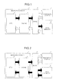
- Fig. 1 is a schematic diagram that shows an outline of a flow of data when a CPU writes the data into a main memory.
- a microprocessor 1 has a CPU 2 and a cache system 3.
- the CPU 2 outputs write data and write address data (hereinafter, address data will be simply referred to as an address) to the cache system 3.
- the write data and the write address are sent to the main memory 6 via a bus control section ("BUSC") 5, and are written into the main memory 6.
- BUSC bus control section
- the solid black arrows in Fig. 1 show the flow of data when the CPU writes the data into the main memory.
- Fig. 2 is a schematic diagram that shows an outline of a flow of data when the CPU reads the data from the main memory.
- the CPU 2 outputs an address of data to be read, that is, a read address, to the cache system 3.
- the read address is sent to the main memory 6 via the bus control section 5.
- the main memory 6 reads data corresponding to the read address.
- the read data is sent to the CPU 2 via the bus control section 5 and the cache system 3.
- the solid black arrows in Fig. 2 show the flow of data when the CPU reads the data from the main memory.
- Fig. 3 is a schematic diagram that shows an outline of a flow of data when the CPU writes the data into a peripheral system.
- the CPU 2 outputs a write data and a write address to the cache system 3.
- the write data and the write address are sent to the peripheral system 7 via the bus control section 5, and are written into this control register or the like.
- the solid black arrows in Fig. 3 show the flow of data when the CPU writes the data into the peripheral system.
- Fig. 4 is a schematic diagram that shows an outline of a flow of data when the CPU reads the data from the peripheral system.
- the CPU 2 outputs a read address to the cache system 3.
- the read address is sent to the peripheral system 7 via the bus control section 5 .
- the peripheral system 7 reads data corresponding to the read address.
- the read data is sent to the CPU 2 via the bus control section 5 and the cache system 3.
- the solid black arrows in Fig. 4 show the flow of data when the CPU reads the data from the peripheral system.
- Fig. 5 is a block diagram that shows a detailed structure of a cache system of a conventional microprocessor. As shown in Fig. 5, the cache system 3 has a tag RAM 31 that stores an identification address of a cache block, and a cache RAM 32 that stores data.
- the cache system 3 has a wait address register (“WAR”) 33, a read address register (“RAR”) 34, a cache write buffer address (“CWBA”) 35, and a store buffer address (“STBA”) 36, as registers that store addresses. Further, the cache system 3 has a wait data register (“WDR”) 37, a cache write buffer (“CWB”) 38, and a store buffer (“STB”) 39, as registers that store data. Further, the cache system 3 has five selectors 41, 43, 44, 45, and 46 , and a tag address comparator 42. Further, the cache system 3 has a cache control section (not shown)that controls the cache system 3.
- Fig. 6 is a diagram that shows a flow of an address and read data when a read access makes a cache hit in the microprocessor shown in Fig. 5.
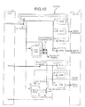
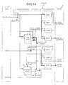
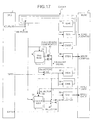
- thick lines show along which routes the address and the data flow (the same applies to Fig. 7 to Fig. 17, and Fig. 20 to Fig. 23).
- the CPU 2 supplies a read address to the tag RAM 31 and the cache RAM 32 via the selector 41.
- the tag address comparator 42 compares a tag address with the read address. When these coincide with each other as a result of the comparison (cache hit), the CPU 2 receives data that has been read by way of the cache RAM 32 in which the addresses coincide, via the selectors 45 and 46. Further, a cache hit signal is asserted.
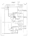
- Fig. 7 is a diagram that shows a flow of an address and read data when a read access makes a cache miss in the microprocessor shown in Fig. 5.
- the CPU 2 supplies a read address to the tag RAM 31 via the selector 41.
- the tag address comparator 42 compares the tag address with the read address . When these do not coincide with each other as a result of the comparison (cache miss) , the read address is stored into the read address register 34.
- the stored read address is output to the bus control section 5 together with a read request, until when the read address is accepted by the bus control section 5.
- this read data is sent to the CPU 2 via the selector 46, and the data is also stored into the cache RAM 32 via the selector 44.
- the cache hit signal is negated. More specifically, a read address is also supplied to the cache RAM 32 from the CPU 32.
- a thin line is used to show a section from the selector 41 to the cache RAM 32 instead of a thick line that shows an address supply route (the same applies to Fig. 15).
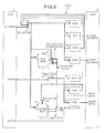
- Fig. 8 is a diagram that shows a flow of an address and read data when a write access makes a cache hit in the microprocessor shown in Fig. 5.
- the CPU 2 supplies a write address to the tag RAM 31 and the cache RAM 32 via the selector 41.
- the tag address comparator 42 compares the tag address with the write address. When these coincide with each other as a result of the comparison (cache hit) , the write address is stored into the cache write buffer address 35 and the store buffer address 36.
- the write data is stored into the cache write buffer 38 and the store buffer 39 via the selector 43.
- the write address stored in the store buffer address 36 and the write data stored in the store buffer 39 are supplied to the bus control section 5 together with a write request.
- the write address stored in the cache write buffer address 35 is supplied to the tag RAM 31 and the cache RAM 32.
- the write data stored in the cache write buffer 38 is written into an area corresponding to the write address of the cache RAM 32. Further, a cache hit signal is asserted.
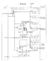
- Fig. 9 is a diagram that shows a flow of an address and read data when a write access makes a cache miss in the microprocessor shown in Fig. 5.
- the CPU 2 supplies a write address to the tag RAM 31 via the selector 41.
- the tag address comparator 42 compares the tag address with the write address. When these do not coincide with each other as a result of the comparison (cache miss), the write address is stored into the store buffer address 36. On the other hand, the write data is stored into the store buffer 39 via the selector 43.
- the write request, the write address, and the write data are output to the bus control section 5 until the bus control section 5 accepts them.
- the cache hit signal is negated. More specifically, a write address is also supplied to the cache RAM 32 from the CPU 32. However, as the cache miss is explained in this case, a thin line is used to show a section from the selector 41 to the cache RAM 32 (the same applies to Fig. 20, Fig. 10, and Fig. 14).
- Fig. 10 to Fig. 13 are diagrams that sequentially show flows of an address and data in this case.
- the CPU 2 makes a write request to the cache system 3, and outputs a write address to the tag RAM 31.
- the tag address comparator 42 compares a tag address with the write address, and when there is a cache miss as a result of the comparison, the write address and write data are stored into the store buffer address 36 and the store buffer 39 respectively. Then, the write request is output to the bus control section 5 (refer to Fig. 10).
- the CPU 2 makes a read request to the cache system 3. Based on this read request, a read address is compared with the address stored in the store buffer address 36. When these addresses coincide with each other, the read address is stored into the wait address register 33. The read address is stored in the wait address register 33 until the preceding write request has been accepted by the bus control section 5 and the operation has been completed (refer to Fig. 11).
- the succeeding read request is executed again.
- the read address is stored into the read address register 34, and the read request and the address are output to the bus control section 5 (refer to Fig. 12).
- the bus control section 5 accepts the read request, and returns the requested data to the cache system 3.
- the returned data is output from the cache system 3 to the CPU 2 (refer to Fig. 13).
- Fig. 14 to Fig. 17 are diagrams that sequentially show flows of an address and data in this case.
- the CPU 2 makes a write request to the cache system 3, and outputs a write address to the tag RAM 31.
- the tag address comparator 42 compares a tag address with the write address, and when there is a cache miss as a result of the comparison, the write address and write data are stored into the store buffer address 36 and the store buffer 39 respectively. Then, the write request is output to the bus control section 5 (refer to Fig. 14).
- the CPU 2 makes a read request to the cache system 3, and supplies a read address to the tag RAM 31.
- the tag address comparator 42 compares the addresses, and when there is a cache miss as a result of this comparison, the read address is stored into the read address register 34.
- the read request and the address are output to the bus control section 5 until the bus control section 5 accepts them (refer to Fig. 15).
- the write request and the read request are output to the bus control section 5 at the same time.
- the bus control section 5 first accepts the read request.
- the bus control section 5 returns the requested data to the cache system 3.
- the returned data is supplied straight to the CPU 2 (refer to Fig. 16).
- the bus control section 5 accepts the write request (refer to Fig. 17).
- the order of the write request and the read request may be reversed in order to increase the processing capacity.
- timer control word register data becomes a read back command when a value of a select counter (“SC") 1 or an SC0 is 11.
- SC select counter
- SC0 select counter
- TCSR0 to 3 a value of the timer control status register
- the data becomes a status latched count value.
- TCSR0 to 3 a value of the timer control status register (TCSR0 to 3) is read when the data is not the read back command, that is, when a value of the SC1 or the SC0 is not 11, the data becomes a count value at that time.
- a microprocessor is provided with a register which stores an address that requires a guarantee of an access order, and an address comparator which compares the address stored in this register with an address of an access request from a CPU.
- the address comparator decides that the two addresses coincide with each other, a preceding access request is executed first, and a succeeding access request is executed after this preceding access request has been executed.
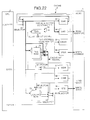
- Fig. 19 is a block diagram that shows a structure example of a cache system of a microprocessor according to the present invention.
- a cache system 8 has a serial address register ("SAR") 81, and a serial address comparator 82.
- SAR serial address register
- the cache system 8 has a tag RAM 31, a cache RAM 32, a wait address register (“WAR”) 33, a read address register (“RAR”) 34, a cache write buffer address (“CWBA”) 35, a store buffer address (“STBA”) 36, a wait data register (“WDR”) 37, a cache write buffer (“CWB”) 38, and a store buffer (STB) 39.
- the cache system 8 has five selectors 41, 43, 44, 45, and 46, and a tag address comparator 42.
- the cache system 8 has a cache control section (not shown) that controls the cache system 8.
- the serial address register 81 is a register which stores an address that requires an access order. For example, when the CPU 2 writes a value of an address that requires the access order as data into the serial address register 81, this address is stored into the serial address register 81.
- the serial address comparator 82 compares an address selected by the selector 41 to be described later with an address stored in the serial address register 81. When the addresses coincide with each other, a serialize hit signal supplied to a cache control section not shown is asserted. When the serialize hit signal has been asserted, the cache control section carries out a control to guarantee the access order. When the addresses do not coincide with each other as a result of the comparison by the serial address comparator 82, the serialize hit signal is negated. In this case, the access order is not guaranteed.
- the wait address register 33 is a register which stores an address when the execution has to wait for some reason.
- the read address register 34 is a register which stores a read address to the buffer control section 5.
- the cache write buffer address 35 is a register which stores a write address to the cache system 8.
- the store buffer address 36 is a register which stores a write address to the bus control section 5.
- the wait data register 37 is a register which stores data when the execution has to wait for some reason.
- the cache write buffer 38 is a register which stores write data to the cache system 8.
- the store buffer 39 is a register which stores write data to the bus control section 5.
- the first register 41 selects one of an address supplied from the CPU 2, an address stored in the wait address register 33, an address stored in the read address register 34, and an address stored in the cache write buffer address 35.
- the address selected by the selector 41 is supplied to the wait address register 33, read address register 34, cache write buffer address 35, or the store buffer address 36. At the same time, this selected address is also supplied to the tag RAM 31, the cache RAM 32, and the tag address comparator 42.
- the cache may have a number of ways (associative cache). In this case, the comparator 42 has comparators of a number equal to the number of ways. Each comparator compares an address selected by the selector 41 with an address stored in the tag RAM 31 of each way. When the addresses coincide with each other as a result of this comparison, a cache hit signal supplied to the cache control section is asserted. When the addresses do not coincide with each other, the cache hit signal is negated.
- the second register 43 selects one of data supplied from the CPU 2 and data stored in the wait data register 37.
- the data selected by the selector 43 is supplied to the wait data register 37, the cache write buffer 38, or the store buffer 39.
- the third selector 44 selects one of read data supplied from the bus control section 5 and data stored in the cache write buffer 38. The data selected by the selector 44 is supplied to the cache RAM 32.
- the fourth selector 45 selects output data from the cache RAM 32 of any one way, based on a result of the comparison by the tag address comparator 42.
- the fifth selector 46 selects either data selected by the fourth selector 45 or read data supplied from the bus control section 5. The data selected by the fifth selector 46 is supplied to the CPU 2.
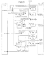
- FIG. 20 to Fig. 23 are diagrams that sequentially show flows of an address and data in this case. An address that requires an access order has been stored in advance in the serial address register 81.
- the CPU 2 makes a write request to the cache system 8, and outputs a write address.
- This write address is supplied to the tag RAM 31 and the tag address comparator 42 via the first selector 41.
- the tag address comparator 42 compares a tag address with the write address, and when there is a cache miss as a result of this comparison, the write address is stored into the store buffer address 36. Further, write data supplied from the CPU 2 is stored into the store buffer 39 via the second selector 43. Then, the write request is output to the bus control section 5 (refer to Fig. 20).
- the CPU 2 makes a read request to the cache system 8, and outputs a read address .
- This read address is supplied to serial address comparator 82.
- the serial address comparator 82 compares the read address with an address stored in the serial address register 81. When the addresses coincide with each other as a result of the comparison, the read address is stored into the wait address register 33. The read address is stored in the wait address register 33 until the preceding write request has been accepted by the bus control section 5 and the operation has been completed (refer to Fig. 21).
- the cache system 8 does not accept requests from the CPU 2 thereafter.
- the succeeding read request is executed again.
- the read address is stored into the read address register 34.
- the read request and the address are output to the bus control section 5 (refer to Fig. 22).
- the bus control section 5 accepts the read request, and returns the requested data to the cache system 8.
- the returned data is output from the cache system 8 to the CPU 2 (refer to Fig. 23).
- the microprocessor is provided with the serial address register 81 and the serial address comparator 82.
- the serial address register 81 stores an address that requires a guarantee of an access order
- the serial address comparator 82 compares an address supplied from the CPU 2 with the address stored in the serial address register 81.
- the succeeding access request becomes in a wait status until when the bus control section 5 has accepted the preceding access request and has completed the operation. Therefore, it is possible to guarantee access order for the access request that requires a guarantee of the access order. Consequently, it becomes possible to guarantee the access order in hardware. As a result, a programmer can carry out programming efficiently without considering a limitation of the access order or the like.
- the present invention is not limited to the embodiment explained above, and it is also possible to modify the embodiment in various ways.
- a structure having a plurality of the serial address registers 81 Based on this arrangement, it becomes possible to guarantee an access order to a plurality of addresses.
- the serial address register 81 can set a size of an address area that requires a guarantee of an order.
- the value stored in the serial address registers 81 may be a pre-set fixed value. When the value stored in the serial address registers 81 is fixed, the control of the cache system 8 becomes easy.
- an address supplied from the CPU is compared with an address that requires a guarantee of an access order.
- these addresses coincide with each other, a preceding access request is executed first, and a succeeding access request is executed after this preceding access request has been executed. Therefore, it is possible to guarantee an access order to the access request that requires a guarantee of the access order. Consequently, it becomes possible to guarantee the access order in hardware. As a result, a programmer can carry out programming efficiently without considering a limitation of the access order or the like.
Landscapes
- Engineering & Computer Science (AREA)
- Theoretical Computer Science (AREA)
- Software Systems (AREA)
- Physics & Mathematics (AREA)
- General Engineering & Computer Science (AREA)
- General Physics & Mathematics (AREA)
- Memory System Of A Hierarchy Structure (AREA)
- Microcomputers (AREA)
- Advance Control (AREA)
- Multi Processors (AREA)
Abstract
Description
Claims (6)
- A microprocessor comprising:a register which stores an address area, the address area requiring a guarantee of an access order; anda comparator which compares the address area held in said register with an address area indicated in an access request from a CPU, and which outputs a signal for executing a succeeding access request after executing a preceding access request when the comparison of address areas indicates that the addresses in the two address areas match each other.
- The microprocessor according to claim 1, wherein the address area stored in said register is fixed.
- The microprocessor according to claim 1 or 2, wherein a size of the address area stored in said register can be set as desired.
- The microprocessor according to claim 1, 2, or 3, wherein a plurality of address areas stored in said register are provided.
- The microprocessor according to any preceding claim, further comprising an n-way associative cache and wherein the comparator is formed by a set of n comparators.
- A method of processing access requests in a microprocessor comprising steps of:storing, in a register, an address area requiring a guarantee of an access order;comparing, in a comparator, an address area received from a CPU of the microprocessor with the address area stored in the register; andoutputting a signal for preserving the order of access requests when addresses in the two address areas match.
Applications Claiming Priority (2)
| Application Number | Priority Date | Filing Date | Title |
|---|---|---|---|
| JP2001216223A JP2003029967A (en) | 2001-07-17 | 2001-07-17 | Microprocessor |
| JP2001216223 | 2001-07-17 |
Publications (3)
| Publication Number | Publication Date |
|---|---|
| EP1278121A2 true EP1278121A2 (en) | 2003-01-22 |
| EP1278121A3 EP1278121A3 (en) | 2004-06-23 |
| EP1278121B1 EP1278121B1 (en) | 2006-11-15 |
Family
ID=19050728
Family Applications (1)
| Application Number | Title | Priority Date | Filing Date |
|---|---|---|---|
| EP02251945A Expired - Lifetime EP1278121B1 (en) | 2001-07-17 | 2002-03-19 | Microprocessor maintaining memory consistency |
Country Status (6)
| Country | Link |
|---|---|
| US (1) | US6823406B2 (en) |
| EP (1) | EP1278121B1 (en) |
| JP (1) | JP2003029967A (en) |
| KR (1) | KR100764581B1 (en) |
| DE (1) | DE60216016T2 (en) |
| TW (1) | TWI222567B (en) |
Families Citing this family (5)
| Publication number | Priority date | Publication date | Assignee | Title |
|---|---|---|---|---|
| US20080201531A1 (en) * | 2006-09-29 | 2008-08-21 | Kornegay Marcus L | Structure for administering an access conflict in a computer memory cache |
| US20080082755A1 (en) * | 2006-09-29 | 2008-04-03 | Kornegay Marcus L | Administering An Access Conflict In A Computer Memory Cache |
| GB2469299B (en) * | 2009-04-07 | 2011-02-16 | Imagination Tech Ltd | Ensuring consistency between a data cache and a main memory |
| JP5482197B2 (en) | 2009-12-25 | 2014-04-23 | 富士通株式会社 | Arithmetic processing device, information processing device, and cache memory control method |
| US8392621B2 (en) * | 2010-06-22 | 2013-03-05 | International Business Machines Corporation | Managing dataflow in a temporary memory |
Family Cites Families (15)
| Publication number | Priority date | Publication date | Assignee | Title |
|---|---|---|---|---|
| JPS62278639A (en) * | 1986-05-27 | 1987-12-03 | Nec Corp | Information processor |
| DE4237417C2 (en) | 1992-03-25 | 1997-01-30 | Hewlett Packard Co | Data processing system |
| US5467473A (en) * | 1993-01-08 | 1995-11-14 | International Business Machines Corporation | Out of order instruction load and store comparison |
| DE69423206T2 (en) | 1994-04-28 | 2000-09-07 | Hewlett-Packard Co., Palo Alto | Computing device with means for forcing the execution of commands in a regular sequence |
| US5666494A (en) * | 1995-03-31 | 1997-09-09 | Samsung Electronics Co., Ltd. | Queue management mechanism which allows entries to be processed in any order |
| US5737636A (en) * | 1996-01-18 | 1998-04-07 | International Business Machines Corporation | Method and system for detecting bypass errors in a load/store unit of a superscalar processor |
| US6006325A (en) | 1996-12-19 | 1999-12-21 | Institute For The Development Of Emerging Architectures, L.L.C. | Method and apparatus for instruction and data serialization in a computer processor |
| DE69725620T2 (en) | 1997-08-06 | 2004-08-12 | Advanced Micro Devices, Inc., Sunnyvale | DEVICE AND METHOD FOR SPECIAL REGISTER ACCESS WITHOUT SERIALIZATION |
| US6148394A (en) | 1998-02-10 | 2000-11-14 | International Business Machines Corporation | Apparatus and method for tracking out of order load instructions to avoid data coherency violations in a processor |
| JPH11249959A (en) | 1998-03-02 | 1999-09-17 | Matsushita Electric Ind Co Ltd | Cache memory control method and apparatus |
| US6266768B1 (en) * | 1998-12-16 | 2001-07-24 | International Business Machines Corporation | System and method for permitting out-of-order execution of load instructions |
| JP3525070B2 (en) * | 1999-01-27 | 2004-05-10 | 松下電器産業株式会社 | Access control device and access method |
| US6412057B1 (en) * | 1999-02-08 | 2002-06-25 | Kabushiki Kaisha Toshiba | Microprocessor with virtual-to-physical address translation using flags |
| US6266767B1 (en) * | 1999-04-22 | 2001-07-24 | International Business Machines Corporation | Apparatus and method for facilitating out-of-order execution of load instructions |
| JP4588158B2 (en) * | 2000-03-28 | 2010-11-24 | 富士通セミコンダクター株式会社 | Semiconductor integrated circuit |
-
2001
- 2001-07-17 JP JP2001216223A patent/JP2003029967A/en active Pending
-
2002
- 2002-03-13 US US10/095,568 patent/US6823406B2/en not_active Expired - Lifetime
- 2002-03-15 TW TW091104977A patent/TWI222567B/en not_active IP Right Cessation
- 2002-03-19 EP EP02251945A patent/EP1278121B1/en not_active Expired - Lifetime
- 2002-03-19 DE DE60216016T patent/DE60216016T2/en not_active Expired - Lifetime
- 2002-04-02 KR KR1020020017909A patent/KR100764581B1/en not_active Expired - Fee Related
Also Published As
| Publication number | Publication date |
|---|---|
| US6823406B2 (en) | 2004-11-23 |
| DE60216016T2 (en) | 2007-04-05 |
| JP2003029967A (en) | 2003-01-31 |
| TWI222567B (en) | 2004-10-21 |
| DE60216016D1 (en) | 2006-12-28 |
| KR20030006937A (en) | 2003-01-23 |
| EP1278121B1 (en) | 2006-11-15 |
| EP1278121A3 (en) | 2004-06-23 |
| US20030018854A1 (en) | 2003-01-23 |
| KR100764581B1 (en) | 2007-10-09 |
Similar Documents
| Publication | Publication Date | Title |
|---|---|---|
| US6131145A (en) | Information processing unit and method for controlling a hierarchical cache utilizing indicator bits to control content of prefetching operations | |
| EP0747816B1 (en) | Method and system for high performance multithread operation in a data processing system | |
| US5737750A (en) | Partitioned single array cache memory having first and second storage regions for storing non-branch and branch instructions | |
| EP0042000B1 (en) | Cache memory in which the data block size is variable | |
| US5689679A (en) | Memory system and method for selective multi-level caching using a cache level code | |
| US5293500A (en) | Parallel processing method and apparatus | |
| US5493669A (en) | Data processor for simultaneously searching two fields of the rename buffer having first and second most recently allogated bits | |
| EP0541216B1 (en) | Data driven processing system | |
| US7073026B2 (en) | Microprocessor including cache memory supporting multiple accesses per cycle | |
| US6779102B2 (en) | Data processor capable of executing an instruction that makes a cache memory ineffective | |
| US5713038A (en) | Microprocessor having register file | |
| US7836253B2 (en) | Cache memory having pipeline structure and method for controlling the same | |
| US6321328B1 (en) | Processor having data buffer for speculative loads | |
| EP0288760A2 (en) | Data processor capable of correctly re-executing instructions | |
| US6785781B2 (en) | Read/write alignment scheme for port reduction of multi-port SRAM cells | |
| EP0436305B1 (en) | System and method for efficiently supporting access to I/O devices through large direct-mapped data caches | |
| US6038642A (en) | Method and system for assigning cache memory utilization within a symmetric multiprocessor data-processing system | |
| US5675765A (en) | Cache memory system with independently accessible subdivided cache tag arrays | |
| EP1030243B1 (en) | Optimized hardware cleaning function for virtual index virtual tag data cache | |
| US6823406B2 (en) | Microprocessor executing a program to guarantee an access order | |
| US6349370B1 (en) | Multiple bus shared memory parallel processor and processing method | |
| US5933856A (en) | System and method for processing of memory data and communication system comprising such system | |
| US6694408B1 (en) | Scalable replacement method and system in a cache memory | |
| KR960005394B1 (en) | Multiprocessor system | |
| JPH06149674A (en) | Information processing apparatus having shared cache memory and block replacement control method thereof |
Legal Events
| Date | Code | Title | Description |
|---|---|---|---|
| PUAI | Public reference made under article 153(3) epc to a published international application that has entered the european phase |
Free format text: ORIGINAL CODE: 0009012 |
|
| AK | Designated contracting states |
Kind code of ref document: A2 Designated state(s): AT BE CH CY DE DK ES FI FR GB GR IE IT LI LU MC NL PT SE TR |
|
| AX | Request for extension of the european patent |
Free format text: AL;LT;LV;MK;RO;SI |
|
| PUAL | Search report despatched |
Free format text: ORIGINAL CODE: 0009013 |
|
| AK | Designated contracting states |
Kind code of ref document: A3 Designated state(s): AT BE CH CY DE DK ES FI FR GB GR IE IT LI LU MC NL PT SE TR |
|
| AX | Request for extension of the european patent |
Extension state: AL LT LV MK RO SI |
|
| 17P | Request for examination filed |
Effective date: 20041215 |
|
| AKX | Designation fees paid |
Designated state(s): DE FR GB |
|
| GRAP | Despatch of communication of intention to grant a patent |
Free format text: ORIGINAL CODE: EPIDOSNIGR1 |
|
| GRAS | Grant fee paid |
Free format text: ORIGINAL CODE: EPIDOSNIGR3 |
|
| GRAA | (expected) grant |
Free format text: ORIGINAL CODE: 0009210 |
|
| AK | Designated contracting states |
Kind code of ref document: B1 Designated state(s): DE FR GB |
|
| REG | Reference to a national code |
Ref country code: GB Ref legal event code: FG4D |
|
| REF | Corresponds to: |
Ref document number: 60216016 Country of ref document: DE Date of ref document: 20061228 Kind code of ref document: P |
|
| ET | Fr: translation filed | ||
| PLBE | No opposition filed within time limit |
Free format text: ORIGINAL CODE: 0009261 |
|
| STAA | Information on the status of an ep patent application or granted ep patent |
Free format text: STATUS: NO OPPOSITION FILED WITHIN TIME LIMIT |
|
| 26N | No opposition filed |
Effective date: 20070817 |
|
| REG | Reference to a national code |
Ref country code: GB Ref legal event code: 732E |
|
| REG | Reference to a national code |
Ref country code: FR Ref legal event code: TP |
|
| PGFP | Annual fee paid to national office [announced via postgrant information from national office to epo] |
Ref country code: GB Payment date: 20090318 Year of fee payment: 8 |
|
| PGFP | Annual fee paid to national office [announced via postgrant information from national office to epo] |
Ref country code: FR Payment date: 20090316 Year of fee payment: 8 |
|
| GBPC | Gb: european patent ceased through non-payment of renewal fee |
Effective date: 20100319 |
|
| REG | Reference to a national code |
Ref country code: FR Ref legal event code: ST Effective date: 20101130 |
|
| PG25 | Lapsed in a contracting state [announced via postgrant information from national office to epo] |
Ref country code: FR Free format text: LAPSE BECAUSE OF NON-PAYMENT OF DUE FEES Effective date: 20100331 |
|
| PG25 | Lapsed in a contracting state [announced via postgrant information from national office to epo] |
Ref country code: GB Free format text: LAPSE BECAUSE OF NON-PAYMENT OF DUE FEES Effective date: 20100319 |
|
| REG | Reference to a national code |
Ref country code: DE Ref legal event code: R082 Ref document number: 60216016 Country of ref document: DE Representative=s name: REICHERT & LINDNER PARTNERSCHAFT PATENTANWAELT, DE |
|
| REG | Reference to a national code |
Ref country code: DE Ref legal event code: R081 Ref document number: 60216016 Country of ref document: DE Owner name: SOCIONEXT INC., YOKOHAMA-SHI, JP Free format text: FORMER OWNER: FUJITSU SEMICONDUCTOR LTD., YOKOHAMA, KANAGAWA, JP Effective date: 20150512 Ref country code: DE Ref legal event code: R082 Ref document number: 60216016 Country of ref document: DE Representative=s name: REICHERT & LINDNER PARTNERSCHAFT PATENTANWAELT, DE Effective date: 20150512 |
|
| PGFP | Annual fee paid to national office [announced via postgrant information from national office to epo] |
Ref country code: DE Payment date: 20200320 Year of fee payment: 19 |
|
| REG | Reference to a national code |
Ref country code: DE Ref legal event code: R119 Ref document number: 60216016 Country of ref document: DE |
|
| PG25 | Lapsed in a contracting state [announced via postgrant information from national office to epo] |
Ref country code: DE Free format text: LAPSE BECAUSE OF NON-PAYMENT OF DUE FEES Effective date: 20211001 |