EP1278060A1 - CCD sensor - Google Patents
CCD sensor Download PDFInfo
- Publication number
- EP1278060A1 EP1278060A1 EP02014253A EP02014253A EP1278060A1 EP 1278060 A1 EP1278060 A1 EP 1278060A1 EP 02014253 A EP02014253 A EP 02014253A EP 02014253 A EP02014253 A EP 02014253A EP 1278060 A1 EP1278060 A1 EP 1278060A1
- Authority
- EP
- European Patent Office
- Prior art keywords
- electric charges
- ccd sensor
- diffusion
- detecting elements
- charge
- Prior art date
- Legal status (The legal status is an assumption and is not a legal conclusion. Google has not performed a legal analysis and makes no representation as to the accuracy of the status listed.)
- Withdrawn
Links
- 238000009792 diffusion process Methods 0.000 claims abstract description 50
- 238000001444 catalytic combustion detection Methods 0.000 claims description 48
- 230000004888 barrier function Effects 0.000 claims description 6
- 238000002347 injection Methods 0.000 claims description 4
- 239000007924 injection Substances 0.000 claims description 4
- 239000011159 matrix material Substances 0.000 claims 1
- 238000009825 accumulation Methods 0.000 description 8
- 238000010586 diagram Methods 0.000 description 7
- 239000004065 semiconductor Substances 0.000 description 5
- 239000000126 substance Substances 0.000 description 5
- GPRLSGONYQIRFK-UHFFFAOYSA-N hydron Chemical compound [H+] GPRLSGONYQIRFK-UHFFFAOYSA-N 0.000 description 4
- 230000003247 decreasing effect Effects 0.000 description 2
- 229910052739 hydrogen Inorganic materials 0.000 description 2
- 239000001257 hydrogen Substances 0.000 description 2
- -1 hydrogen ions Chemical class 0.000 description 2
- 239000000758 substrate Substances 0.000 description 2
- 238000010276 construction Methods 0.000 description 1
- 230000000694 effects Effects 0.000 description 1
- 230000010354 integration Effects 0.000 description 1
- 150000002500 ions Chemical class 0.000 description 1
- 239000007788 liquid Substances 0.000 description 1
- 239000002184 metal Substances 0.000 description 1
- 238000000034 method Methods 0.000 description 1
- 229910052710 silicon Inorganic materials 0.000 description 1
- 239000010703 silicon Substances 0.000 description 1
Images



Classifications
-
- H—ELECTRICITY
- H10—SEMICONDUCTOR DEVICES; ELECTRIC SOLID-STATE DEVICES NOT OTHERWISE PROVIDED FOR
- H10D—INORGANIC ELECTRIC SEMICONDUCTOR DEVICES
- H10D44/00—Charge transfer devices
- H10D44/40—Charge-coupled devices [CCD]
- H10D44/45—Charge-coupled devices [CCD] having field effect produced by insulated gate electrodes
- H10D44/454—Output structures
-
- G—PHYSICS
- G01—MEASURING; TESTING
- G01N—INVESTIGATING OR ANALYSING MATERIALS BY DETERMINING THEIR CHEMICAL OR PHYSICAL PROPERTIES
- G01N27/00—Investigating or analysing materials by the use of electric, electrochemical, or magnetic means
- G01N27/26—Investigating or analysing materials by the use of electric, electrochemical, or magnetic means by investigating electrochemical variables; by using electrolysis or electrophoresis
- G01N27/403—Cells and electrode assemblies
- G01N27/414—Ion-sensitive or chemical field-effect transistors, i.e. ISFETS or CHEMFETS
- G01N27/4148—Integrated circuits therefor, e.g. fabricated by CMOS processing
-
- H—ELECTRICITY
- H10—SEMICONDUCTOR DEVICES; ELECTRIC SOLID-STATE DEVICES NOT OTHERWISE PROVIDED FOR
- H10F—INORGANIC SEMICONDUCTOR DEVICES SENSITIVE TO INFRARED RADIATION, LIGHT, ELECTROMAGNETIC RADIATION OF SHORTER WAVELENGTH OR CORPUSCULAR RADIATION
- H10F39/00—Integrated devices, or assemblies of multiple devices, comprising at least one element covered by group H10F30/00, e.g. radiation detectors comprising photodiode arrays
- H10F39/10—Integrated devices
- H10F39/12—Image sensors
- H10F39/15—Charge-coupled device [CCD] image sensors
- H10F39/153—Two-dimensional or three-dimensional array CCD image sensors
- H10F39/1534—Interline transfer
Definitions
- the present invention is directed to a CCD sensor.
- An apparatus capable of acquiring two-dimensional information by employing a CCD is known from, for instance, European Patent Publication EP-0881486 entitled “Method For Measuring Physical Phenomenon, or Chemical Phenomenon, and Equipment Thereof" .
- a sensor used in this measuring apparatus such a CCD sensor is employed which is arranged by a plurality of physical/chemical sensors (unit sensors) sensible to physical/chemical phenomena, and also, a plurality of CCDs which transfer electric signal charges produced from these plural unit sensors.
- Fig. 3 is a diagram for schematically indicating a structure of an upper surface of a CCD sensor which measures, for example, a two-dimensional distributing condition of pH.
- reference numeral 1 indicates a CCD sensor.
- This CCD sensor 1 is constituted by a plurality of unit elements (unit sensors) 2 sensible to hydrogen ions. While the upper surfaces of the respective unit elements 2 are covered by pH responsive films capable of sensing (responding) with respect to hydrogen ions corresponding to a measuring object, potentials are produced at boundary surfaces between the pH response film and a liquid in response to an amount of hydrogen-ion concentration, and a magnitude (namely, pH) of the hydrogen ion concentration is converted into an electric charge signal by utilizing a change of this potential.
- Reference numeral 6 shows a charge transfer portion for transferring electric charge signals produced in the respective unit sensors 2.
- This charge transfer portion 6 is arrayed by a plurality of vertical CCDs 7 and a single horizontal CCD 8, while the vertical CCDs 7 are arranged by a plurality of CCDs.
- reference numeral 9 represents a signal output portion for outputting a signal derived from the horizontal CCD 8.
- Reference numeral 20 represents a diffusion portion of the signal output portion 9.
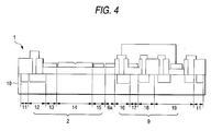
- Fig. 4 illustratively shows a basic structure of the above-explained CCD sensor 1.
- reference numeral 10 indicates a semiconductor substrate made of, for instance, p type Si (silicon), the thickness of which is selected to be on the order of 500 micrometers.
- a channel stopper 11, a charge supplying portion 12, a charge injection control portion 13, a sensor portion 14 functioning as a charge converting portion, a barrier portion 15, a CCD 6a which constitutes the charge transfer portion 6, a floating diffusion 16, a reset gate 17, a reset drain 18, and an output transistor 19 having an MOS structure are formed on the above-described semiconductor substrate 10.
- a single piece of unit sensor 2 is constituted by the respective members such as the charge supply portion 12, the charge injection control portion 13, the sensor portion 14, and the barrier portion 15.
- the sensor portion 14 constructs such a potential well which is constituted in such a manner that a depth of this potential well is changed in response to a magnitude of hydrogen-ion concentration.
- the signal output portion 9 is constituted by the respective members such as the floating diffusion 16, the reset gate 17, the reset drain 18, and the output transistor 19.
- the potential of the charge supplying portion 12 is set to a high potential (namely, arrow direction is high potential), and electric charges 21 are not injected into the sensor portion 14.
- the barrier portion 15 is closed so as to stop the flow-in operation of the charges.
- the potential of the floating diffusion 16 is determined based upon an amount of such transferred electric charges 21, this potential is inputted to the gate portion of the output transistor 19 having the MOS structure, and a drain current of this output transistor 19 is measured by a source follower circuit.
- the electric charges appeared in the detecting elements 2 arranged in the two-dimensional manner are continuously carried to the diffusion portion 20 of the signal output portion 9, and then, are converted into the voltage by this diffusion portion 20.
- This voltage may be outputted outside this CCD.
- S/N signal-to-noise ratio
- the areas of the respective detecting elements 2 may be increased so as to carry a large amount of electric charges.
- potential inclinations (fringe effect) at the detecting elements 2 are not involved, there is a limitation in increasing of the above-described areas of these detecting elements 2. As a result, it is practically difficult to achieve sufficiently high S/N.
- the present invention has been made to solve the above-describedproblem, and therefore, has an object to provide such a CCD sensor capable of performing a high-precision measuring operation even when signal levels derived from detecting elements are low, while maintaining a wide dynamic range.
- a CCD sensor is featured by that in a CCD sensor in which electric charges derived from a plurality of detecting elements are outputted from a signal output portion, two diffusion portions are provided in a parallel manner to each other in the signal output portion, and electric charges. outputted from a designated detecting element are accumulated into one of these two diffusion portions so as to output the accumulated electric charges.
- the CCD sensor since the electric charges derived from the designated detecting element are accumulated so as to be produced, even when the signal levels acquired in this designated detecting element are low, the CCD sensor can perform the measuring operation in high precision and the dynamic range thereof can be made wide.
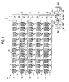
- Fig. 1 and Fig. 2 indicate a CCD sensor 1A according to an embodiment mode of the present invention.
- This CCD sensor 1A of the present invention owns such a large different structure, as compared with that of the above-explained CCD sensor 1 shown in Fig. 3. That is, while two sets of diffusion portions 22A and 22B are provided in a parallel manner to each other in a signal output portion 9, outputs (electric charges) of a designated detecting element 2 are accumulated into one diffusion portion 22A to output the accumulated electric charges.
- reference numerals 22A and 22B indicate diffusion portions which are coupled to a diffusion portion 20 provided on the side of an output of a horizontal CCD 8, these diffusion portions 22A and 22B are arranged in a parallel manner to each other.
- One diffusion portion 22A constitutes a charge-accumulation diffusion portion; and the other diffusion portion 22B constitutes a normal charge-outputting diffusion portion.
- On an edge portion of each of these diffusion portions 22A and 22B both a floating diffusion 23A and another floating diffusion 23B are formed, while reset gates 24A/24B, reset drains 25A/25B, and output transistors 26A/26B are electrically connected to these floating diffusions 23A/23B.
- reference numeral 27 denotes a control portion for controlling the reset gates 24A and 24B. It should be noted that symbols “H” and “L” in Fig. 2 represent two phase electrodes used when the CCD sensor 1A is driven in a two phase mode.
- the charge electrics derived from the four detecting elements 2 located in the region 28, which are inputted into the charge-accumulation diffusion portion 22A, are stored only preset times, while the floating diffusion 23A connected to this charge-accumulation diffusion portion 22A is not reset every time. Thereafter, these electric charges are outputted from this charge-accumulation diffusion portion 22A so as to produce an image signal.
- these small electric charges are integrated with each other only preset times, so that the integrated electric charges may become a large signal and the resulting S/N may be improved. As a consequence, such a specific region which is wanted to be observed can be clearly observed.
- the two-dimensional distribution of pH is observed by the CCD sensor 1A.
- the present invention is not limited to the above-described embodiment mode, but may be accomplished by that since the structure of the detecting elements 2 is properly changed, various sorts of chemical phenomena as well as various kinds of physical phenomena may be observed.
- the CCD sensor in which the electric charges derived from a plurality of detecting elements are outputted from the signal output portion, two diffusion portions are provided in a parallel manner to each other in the signal output portion, and the electric charges outputted from the designated detecting element are accumulated into one of these two diffusion portions so as to output the accumulated electric charges.
- the CCD sensor can perform the measuring operation in high precision, while the dynamic range thereof can be widened. As a result, the specific region can be displayed as the high-precision image.
Landscapes
- Chemical & Material Sciences (AREA)
- Engineering & Computer Science (AREA)
- Microelectronics & Electronic Packaging (AREA)
- Health & Medical Sciences (AREA)
- Life Sciences & Earth Sciences (AREA)
- Electrochemistry (AREA)
- Molecular Biology (AREA)
- Chemical Kinetics & Catalysis (AREA)
- Computer Hardware Design (AREA)
- Physics & Mathematics (AREA)
- Analytical Chemistry (AREA)
- Biochemistry (AREA)
- General Health & Medical Sciences (AREA)
- General Physics & Mathematics (AREA)
- Immunology (AREA)
- Pathology (AREA)
- Solid State Image Pick-Up Elements (AREA)
- Radiation Pyrometers (AREA)
Abstract
In a CCD sensor in which electric charges derived from
a plurality of detecting elements 2 are outputted from a signal
output portion 9, two diffusion portions 22A and 22B are provided
in a parallel manner to each other in the signal output portion
9, and electric charges outputted from a designated detecting
element 2 are accumulated into one diffusion portions 22A so
as to output the accumulated electric charges. Even in such
a case that signal levels derived from detecting elements are
low, such a CCD sensor capable of performing a high-precision
measuring operation is provided, while a dynamic range of the
CCD sensor is widened.
Description
- The present invention is directed to a CCD sensor.
- An apparatus capable of acquiring two-dimensional information by employing a CCD is known from, for instance, European Patent Publication EP-0881486 entitled "Method For Measuring Physical Phenomenon, or Chemical Phenomenon, and Equipment Thereof" . As a sensor used in this measuring apparatus, such a CCD sensor is employed which is arranged by a plurality of physical/chemical sensors (unit sensors) sensible to physical/chemical phenomena, and also, a plurality of CCDs which transfer electric signal charges produced from these plural unit sensors.
- Fig. 3 is a diagram for schematically indicating a structure of an upper surface of a CCD sensor which measures, for example, a two-dimensional distributing condition of pH. In this drawing,
reference numeral 1 indicates a CCD sensor. ThisCCD sensor 1 is constituted by a plurality of unit elements (unit sensors) 2 sensible to hydrogen ions. While the upper surfaces of therespective unit elements 2 are covered by pH responsive films capable of sensing (responding) with respect to hydrogen ions corresponding to a measuring object, potentials are produced at boundary surfaces between the pH response film and a liquid in response to an amount of hydrogen-ion concentration, and a magnitude (namely, pH) of the hydrogen ion concentration is converted into an electric charge signal by utilizing a change of this potential. While, for example, 10 pieces of theseunit sensors 2 are provided along a direction indicated by an arrow 4 so as to constitute asensor column 3, for instance, 5 sets of thesesensor columns 3 are arrayed along a direction indicated by an arrow 5 which is located perpendicular to the above-described arrow 4 so as to arrange the CCD sensor. -
Reference numeral 6 shows a charge transfer portion for transferring electric charge signals produced in therespective unit sensors 2. Thischarge transfer portion 6 is arrayed by a plurality ofvertical CCDs 7 and a singlehorizontal CCD 8, while thevertical CCDs 7 are arranged by a plurality of CCDs. Also,reference numeral 9 represents a signal output portion for outputting a signal derived from thehorizontal CCD 8.Reference numeral 20 represents a diffusion portion of thesignal output portion 9. - Fig. 4 illustratively shows a basic structure of the above-explained
CCD sensor 1. In this drawing,reference numeral 10 indicates a semiconductor substrate made of, for instance, p type Si (silicon), the thickness of which is selected to be on the order of 500 micrometers. - A channel stopper 11, a
charge supplying portion 12, a chargeinjection control portion 13, asensor portion 14 functioning as a charge converting portion, abarrier portion 15, aCCD 6a which constitutes thecharge transfer portion 6, afloating diffusion 16, areset gate 17, areset drain 18, and anoutput transistor 19 having an MOS structure are formed on the above-describedsemiconductor substrate 10. - Then, a single piece of
unit sensor 2 is constituted by the respective members such as thecharge supply portion 12, the chargeinjection control portion 13, thesensor portion 14, and thebarrier portion 15. As will be later discussed more in detail, thesensor portion 14 constructs such a potential well which is constituted in such a manner that a depth of this potential well is changed in response to a magnitude of hydrogen-ion concentration. Also, thesignal output portion 9 is constituted by the respective members such as thefloating diffusion 16, thereset gate 17, thereset drain 18, and theoutput transistor 19. - Now, a principle idea of measuring operations of the above-described
unit sensor 2 will be explained with reference to a potential diagram indicated in Fig. 5. When the measuring operation is carried out, a pulse voltage is applied to thecharge supplying portion 12, thebarrier portion 15, and thereset gate 17, whereas a DC voltage is applied to other electrodes except for thefloating diffusion 16. - On the other hand, in an MOS structure using a p type semiconductor, the following fact is normally known. That is, since a positive voltage is applied to a metal electrode of the MOS structure, a depletion layer is formed on a boundary surface between an insulating film and the semiconductor in response to this positive voltage. As a consequence, while this phenomenon is used, potential states are produced in the vicinity of the boundary surface between the semiconductor and the insulating film, as represented in Fig. 5.
- In a state as indicated in Fig. 5A, the potential of the
charge supplying portion 12 is set to a high potential (namely, arrow direction is high potential), andelectric charges 21 are not injected into thesensor portion 14. - In a state as indicated in Fig. 5B, since the potential of the
charge supplying unit 12 is decreased, theelectric charges 21 are injected into thesensor portion 14. - In a state as indicated in Fig. 5C, since the potential of the
charge supplying unit 12 is increased, theelectric charges 21 which have been cut off by the chargeinjection control portion 13 are stored into thesensor portion 14. - In a state as shown in Fig. 5D, since the potential of the
barrier portion 15 is increased, theelectric charges 21 which have been stored in thesensor portion 14 are transferred to thefloating diffusion 16. - In a state as shown in Fig. 5E, after all of the
electric charges 21 of thesensor portion 14 have been transferred to thefloating diffusion 16, thebarrier portion 15 is closed so as to stop the flow-in operation of the charges. At this stage, the potential of the floatingdiffusion 16 is determined based upon an amount of such transferredelectric charges 21, this potential is inputted to the gate portion of theoutput transistor 19 having the MOS structure, and a drain current of thisoutput transistor 19 is measured by a source follower circuit. - In a state as indicated in Fig. 5F, after the potential of the floating
diffusion 16 has been read, thereset gate 17 is turned ON so as to reset the potential of the floating diffusion to the potential of thereset drain 18. Since this reset operation is performed, the potential state is again returned to the above-explained state shown in Fig. 5A. In other words, since the operations defined from the state of Fig. 5A to the state of Fig. 5F are repeatedly carried out, the electric charges can be derived outside the MOS structure. - In accordance with the CCD sensor having the above-described structure, phenomena occurred at a plurality of different positions can be measured at the same time. Since the magnitude of the hydrogen ion concentration is converted into the electric charges, either a one-dimensional distribution of pH or a two-dimensional distribution of pH can be easily acquired as an image by employing the
charge transfer portion 6 constituted by a plurality ofCCDs 6a. Furthermore, electric charges indicative of information as to plural points are stored, so that a very weak signal can be amplified. Accordingly, a very small change occurred in a phenomenon may also be firmly grasped. - As previously explained, in such a case that the two-dimensional information is obtained by employing the CCD, the electric charges appeared in the detecting
elements 2 arranged in the two-dimensional manner are continuously carried to thediffusion portion 20 of thesignal output portion 9, and then, are converted into the voltage by thisdiffusion portion 20. This voltage may be outputted outside this CCD. In such a case that a chemical amount such as ion concentration, or a physical amount such as a temperature, which are wanted to be measured, constitutes only a portion of an entire amount, and furthermore, a signal amount is small, S/N (signal-to-noise ratio) is necessarily determined based upon performance of an FET of the above-explaineddiffusion portion 20. - Under such a circumstance, the following idea may be conceived. That is, the areas of the respective detecting
elements 2 may be increased so as to carry a large amount of electric charges. In this case, while potential inclinations (fringe effect) at the detectingelements 2 are not involved, there is a limitation in increasing of the above-described areas of these detectingelements 2. As a result, it is practically difficult to achieve sufficiently high S/N. - The present invention has been made to solve the above-describedproblem, and therefore, has an object to provide such a CCD sensor capable of performing a high-precision measuring operation even when signal levels derived from detecting elements are low, while maintaining a wide dynamic range.
- To achieve the above-explained object, a CCD sensor, according to the present invention, is featured by that in a CCD sensor in which electric charges derived from a plurality of detecting elements are outputted from a signal output portion, two diffusion portions are provided in a parallel manner to each other in the signal output portion, and electric charges. outputted from a designated detecting element are accumulated into one of these two diffusion portions so as to output the accumulated electric charges.
- In the CCD sensor with employment of the above-explained structure, since the electric charges derived from the designated detecting element are accumulated so as to be produced, even when the signal levels acquired in this designated detecting element are low, the CCD sensor can perform the measuring operation in high precision and the dynamic range thereof can be made wide.
-
- Fig. 1 is a diagram for schematically showing a structure of a CCD sensor according to the present invention;
- Fig. 2 is an enlarged diagram for showing a structure of a signal output portion of the above-described CCD sensor;
- Fig. 3 is a diagram for schematically indicating the structure of the conventional CCD sensor;
- Fig. 4 is a diagram for schematically indicating the construction of the conventional CCD sensor; and
- Fig. 5 is an explanatory diagram for explaining the measuring principle idea of the conventional CCD sensor.
-
- Referring now to drawings, the present invention will be described in detail. Fig. 1 and Fig. 2 indicate a
CCD sensor 1A according to an embodiment mode of the present invention. ThisCCD sensor 1A of the present invention owns such a large different structure, as compared with that of the above-explainedCCD sensor 1 shown in Fig. 3. That is, while two sets ofdiffusion portions signal output portion 9, outputs (electric charges) of a designated detectingelement 2 are accumulated into onediffusion portion 22A to output the accumulated electric charges. - In other words, as shown in Fig. 1 and Fig. 2,
reference numerals diffusion portion 20 provided on the side of an output of ahorizontal CCD 8, thesediffusion portions diffusion portion 22A constitutes a charge-accumulation diffusion portion; and theother diffusion portion 22B constitutes a normal charge-outputting diffusion portion. On an edge portion of each of thesediffusion portions diffusion 23A and another floatingdiffusion 23B are formed, whilereset gates 24A/24B, reset drains 25A/25B, andoutput transistors 26A/26B are electrically connected to these floatingdiffusions 23A/23B. Then,reference numeral 27 denotes a control portion for controlling thereset gates CCD sensor 1A is driven in a two phase mode. - Next, operations of the
CCD sensor 1 having the above-described structure will now be explained. For instance, in Fig. 1, it is so assumed that signals derived from 4 detectingelements 2 located in such a region indicated by a dot and dashline 28 are accumulated. Electric charges which are derived from all of these detectingelements 2 including the detectingelements 2 in the above-describedregion 28 are entered via both thevertical CCD 7 and thehorizontal CCD 8 into thediffusion portion 20 of thesignal output portion 9. Then, the respective electric charges entered into thediffusion portion 20 may be allocated to the charge-accumulation diffusion portion 22A and the normal charge-outputtingdiffusion portion 22B by switching magnitudes (heights) of voltages at the electrodes "H" and "L" in thisdiffusion portion 20. In this case, only the electric charges outputted from the four detectingelements 2 located in the previously designatedregion 28 are inputted into the charge-accumulation diffusion portion 22A, whereas electric charges outputted from all of the detectingelements 2 which contain the four detectingelements 2 within the designatedregion 28 are inputted into the normal charge-outputtingdiffusion portion 22B except when they are transferred to the charge-accumulation diffusion portion 22A for accumulation. - Then, the electric charges derived from all of the detecting
elements 2, which are entered into the normal charge-outputtingdiffusion portion 22B, are outputted therefrom every time thereset gate 24B is operated so as to produce an image signal in a similar manner to the operations of theconventional CCD sensor 1. - On the other hand, the charge electrics derived from the four detecting
elements 2 located in theregion 28, which are inputted into the charge-accumulation diffusion portion 22A, are stored only preset times, while the floatingdiffusion 23A connected to this charge-accumulation diffusion portion 22A is not reset every time. Thereafter, these electric charges are outputted from this charge-accumulation diffusion portion 22A so as to produce an image signal. As a result, even when the electric charges derived from the four detectingelements 2 located in thisregion 28 are small, these small electric charges are integrated with each other only preset times, so that the integrated electric charges may become a large signal and the resulting S/N may be improved. As a consequence, such a specific region which is wanted to be observed can be clearly observed. - Then, while a total integration time of the electric charges within the
set region 28 may be properly set, and/or the area of thisregion 28 may be properly increased/decreased, such a measuring operation with a wide dynamic range may be carried out without lowering the transfer efficiency in theCCD sensor 1A. - In the above-described embodiment mode, the two-dimensional distribution of pH is observed by the
CCD sensor 1A. However, the present invention is not limited to the above-described embodiment mode, but may be accomplished by that since the structure of the detectingelements 2 is properly changed, various sorts of chemical phenomena as well as various kinds of physical phenomena may be observed. - As previously described, in accordance with the present invention, in the CCD sensor in which the electric charges derived from a plurality of detecting elements are outputted from the signal output portion, two diffusion portions are provided in a parallel manner to each other in the signal output portion, and the electric charges outputted from the designated detecting element are accumulated into one of these two diffusion portions so as to output the accumulated electric charges. As a consequence, even when the signal levels acquired by these designated detecting elements are low, the CCD sensor can perform the measuring operation in high precision, while the dynamic range thereof can be widened. As a result, the specific region can be displayed as the high-precision image.
Claims (5)
- A CCD sensor in which electric charges derived from a plurality of detecting elements are outputted from a signal output portion, wherein:two diffusion portions are provided in a parallel manner to each other in said signal output portion; and electric charges outputted from a designated detecting element are accumulated into one of said two diffusion portions so as to output the accumulated electric charges.
- A CCD sensor comprising:wherein said signal output portion has two diffusion portions provided in a parallel manner to each other, anda plurality of detecting elements being arranged as a matrix;a charge transfer portion for transferring electric charge signals produced in said detecting elements; anda signal output portion for outputting a signal derived from the charge transfer portion,
electric charges outputted from designated detecting elements are accumulated into one of said two diffusion portions so as to output the accumulated electric charges. - The CCD sensor as claimed in claim 2, wherein each of said detecting elements includes a charge supply portion, a charge injection control portion, a sensor portion, and a barrier portion.
- The CCD sensor as claimed in claim 2, wherein said charge transfer portion includes a plurality of CCDs.
- The CCD sensor as claimed in claim 2, wherein each diffusion portion has a floating diffusion formed at edge portion being electrically connected to a reset gate, a reset drain and an output transistor.
Applications Claiming Priority (2)
| Application Number | Priority Date | Filing Date | Title |
|---|---|---|---|
| JP2001198119A JP2003014691A (en) | 2001-06-29 | 2001-06-29 | CCD sensor |
| JP2001198119 | 2001-06-29 |
Publications (1)
| Publication Number | Publication Date |
|---|---|
| EP1278060A1 true EP1278060A1 (en) | 2003-01-22 |
Family
ID=19035615
Family Applications (1)
| Application Number | Title | Priority Date | Filing Date |
|---|---|---|---|
| EP02014253A Withdrawn EP1278060A1 (en) | 2001-06-29 | 2002-06-26 | CCD sensor |
Country Status (3)
| Country | Link |
|---|---|
| US (1) | US7015963B2 (en) |
| EP (1) | EP1278060A1 (en) |
| JP (1) | JP2003014691A (en) |
Cited By (2)
| Publication number | Priority date | Publication date | Assignee | Title |
|---|---|---|---|---|
| EP1669749A1 (en) * | 2004-12-10 | 2006-06-14 | Horiba, Ltd. | FET based method and apparatus for measuring physical or chemical phenomena |
| US8279315B2 (en) | 2005-04-12 | 2012-10-02 | Planmeca Oy | CCD sensor and method for expanding dynamic range of CCD sensor |
Families Citing this family (3)
| Publication number | Priority date | Publication date | Assignee | Title |
|---|---|---|---|---|
| JP2006284225A (en) * | 2005-03-31 | 2006-10-19 | Horiba Ltd | Potential measuring method and measuring instrument |
| JP4641444B2 (en) * | 2005-03-31 | 2011-03-02 | 株式会社堀場製作所 | Potential measurement device for physical or chemical phenomena |
| US7977660B2 (en) * | 2007-08-14 | 2011-07-12 | General Electric Company | Article, device, and method |
Citations (5)
| Publication number | Priority date | Publication date | Assignee | Title |
|---|---|---|---|---|
| US4803531A (en) * | 1987-09-18 | 1989-02-07 | Tektronix, Inc. | Imaging charge-coupled device having an all parallel output |
| EP0559155A1 (en) * | 1992-03-04 | 1993-09-08 | Sony Corporation | Charge-to-voltage converter |
| EP0881486A2 (en) * | 1997-05-29 | 1998-12-02 | Horiba, Ltd. | Method for measuring physical phenomena or chemical phenomena and equipment thereof |
| JP2001033274A (en) * | 1999-07-23 | 2001-02-09 | Horiba Ltd | Physical/chemical two-dimentional distribution measuring device |
| EP1130389A1 (en) * | 2000-02-29 | 2001-09-05 | Horiba, Ltd. | Molecular recognition type chemical CCD sensor |
Family Cites Families (3)
| Publication number | Priority date | Publication date | Assignee | Title |
|---|---|---|---|---|
| KR930005746B1 (en) * | 1990-10-13 | 1993-06-24 | 금성일렉트론 주식회사 | Zigzag Interline Solid State Imaging Device |
| US5452004A (en) * | 1993-06-17 | 1995-09-19 | Litton Systems, Inc. | Focal plane array imaging device with random access architecture |
| JP3262441B2 (en) * | 1994-02-04 | 2002-03-04 | キヤノン株式会社 | Linear image sensor and image reading device |
-
2001
- 2001-06-29 JP JP2001198119A patent/JP2003014691A/en active Pending
-
2002
- 2002-06-26 EP EP02014253A patent/EP1278060A1/en not_active Withdrawn
- 2002-06-27 US US10/183,050 patent/US7015963B2/en not_active Expired - Fee Related
Patent Citations (5)
| Publication number | Priority date | Publication date | Assignee | Title |
|---|---|---|---|---|
| US4803531A (en) * | 1987-09-18 | 1989-02-07 | Tektronix, Inc. | Imaging charge-coupled device having an all parallel output |
| EP0559155A1 (en) * | 1992-03-04 | 1993-09-08 | Sony Corporation | Charge-to-voltage converter |
| EP0881486A2 (en) * | 1997-05-29 | 1998-12-02 | Horiba, Ltd. | Method for measuring physical phenomena or chemical phenomena and equipment thereof |
| JP2001033274A (en) * | 1999-07-23 | 2001-02-09 | Horiba Ltd | Physical/chemical two-dimentional distribution measuring device |
| EP1130389A1 (en) * | 2000-02-29 | 2001-09-05 | Horiba, Ltd. | Molecular recognition type chemical CCD sensor |
Non-Patent Citations (1)
| Title |
|---|
| PATENT ABSTRACTS OF JAPAN vol. 2000, no. 19 5 June 2001 (2001-06-05) * |
Cited By (3)
| Publication number | Priority date | Publication date | Assignee | Title |
|---|---|---|---|---|
| EP1669749A1 (en) * | 2004-12-10 | 2006-06-14 | Horiba, Ltd. | FET based method and apparatus for measuring physical or chemical phenomena |
| US7424372B2 (en) | 2004-12-10 | 2008-09-09 | Horiba, Ltd. | Method and apparatus for measuring physical or chemical phenomena |
| US8279315B2 (en) | 2005-04-12 | 2012-10-02 | Planmeca Oy | CCD sensor and method for expanding dynamic range of CCD sensor |
Also Published As
| Publication number | Publication date |
|---|---|
| JP2003014691A (en) | 2003-01-15 |
| US7015963B2 (en) | 2006-03-21 |
| US20030001583A1 (en) | 2003-01-02 |
Similar Documents
| Publication | Publication Date | Title |
|---|---|---|
| US8388893B2 (en) | Combined detector | |
| US10481123B2 (en) | Ion-sensing charge-accumulation circuits and methods | |
| JP4231560B2 (en) | Method and apparatus for electrochemical measurement of chemical quantity distribution | |
| KR101087565B1 (en) | Photodetector and spatial information detection device using same | |
| US9960253B2 (en) | Chemically sensitive sensor with lightly doped drains | |
| US6294133B1 (en) | Multiple detecting apparatus for physical phenomenon and/or chemical phenomenon | |
| CN100498206C (en) | Electrosatatic capacity detector | |
| EP1870703A1 (en) | Cumulative chemical/physical phenomenon detecting apparatus | |
| WO2003042683A1 (en) | Fet type sensor, ion density detecting method comprising this sensor, and base sequence detecting method | |
| US10684251B2 (en) | Ion sensitive field effect transistor (ISFET) having higher sensitivity in response to dynamic biasing | |
| US6824660B2 (en) | Molecular recognition type chemical CCD | |
| US7015963B2 (en) | CCD sensor incorporating parallel diffusion regions within the output | |
| CN114631188A (en) | Photoelectric sensor and distance measuring system using same | |
| RU2539038C1 (en) | Dna sequencing method and device therefor (versions) | |
| JP2012202864A (en) | Isfet and isfet array | |
| US5892251A (en) | Apparatus for transferring electric charges | |
| US4644572A (en) | Fill and spill for charge input to a CCD | |
| US5357128A (en) | Charge detecting device | |
| JP4852752B2 (en) | Chemical / physical phenomenon detector | |
| Futagawa et al. | $1024\times 1024$ Pixel Charge-Transfer-Type Hydrogen Ion Image Sensor | |
| JP4308374B2 (en) | Chemical quantity two-dimensional distribution measuring device | |
| CN116635714B (en) | Ion sensor and method for manufacturing ion sensor | |
| JP2022053829A (en) | Detection device and detection method | |
| Mimura et al. | CCD based pH imaging sensor | |
| JPH02119266A (en) | Solid-state image sensing device of vertical type overflow drain structure |
Legal Events
| Date | Code | Title | Description |
|---|---|---|---|
| PUAI | Public reference made under article 153(3) epc to a published international application that has entered the european phase |
Free format text: ORIGINAL CODE: 0009012 |
|
| AK | Designated contracting states |
Kind code of ref document: A1 Designated state(s): AT BE CH CY DE DK ES FI FR GB GR IE IT LI LU MC NL PT SE TR |
|
| AX | Request for extension of the european patent |
Free format text: AL;LT;LV;MK;RO;SI |
|
| 17P | Request for examination filed |
Effective date: 20030702 |
|
| AKX | Designation fees paid |
Designated state(s): DE FR GB |
|
| 17Q | First examination report despatched |
Effective date: 20061214 |
|
| STAA | Information on the status of an ep patent application or granted ep patent |
Free format text: STATUS: THE APPLICATION IS DEEMED TO BE WITHDRAWN |
|
| 18D | Application deemed to be withdrawn |
Effective date: 20090103 |