EP1274972B1 - Capacitance level measurement circuit and system - Google Patents
Capacitance level measurement circuit and system Download PDFInfo
- Publication number
- EP1274972B1 EP1274972B1 EP01932553A EP01932553A EP1274972B1 EP 1274972 B1 EP1274972 B1 EP 1274972B1 EP 01932553 A EP01932553 A EP 01932553A EP 01932553 A EP01932553 A EP 01932553A EP 1274972 B1 EP1274972 B1 EP 1274972B1
- Authority
- EP
- European Patent Office
- Prior art keywords
- probe
- capacitor
- capacitance
- circuit
- port
- Prior art date
- Legal status (The legal status is an assumption and is not a legal conclusion. Google has not performed a legal analysis and makes no representation as to the accuracy of the status listed.)
- Expired - Lifetime
Links
- 238000005259 measurement Methods 0.000 title claims abstract description 46
- 239000000523 sample Substances 0.000 claims abstract description 133
- 239000003990 capacitor Substances 0.000 claims abstract description 113
- 230000003071 parasitic effect Effects 0.000 claims abstract description 26
- 239000000463 material Substances 0.000 claims description 31
- 230000008878 coupling Effects 0.000 claims description 7
- 238000010168 coupling process Methods 0.000 claims description 7
- 238000005859 coupling reaction Methods 0.000 claims description 7
- 238000000034 method Methods 0.000 claims description 7
- 230000004323 axial length Effects 0.000 claims 2
- 239000004020 conductor Substances 0.000 description 24
- 239000007788 liquid Substances 0.000 description 8
- 239000012530 fluid Substances 0.000 description 6
- 230000006870 function Effects 0.000 description 6
- 230000008859 change Effects 0.000 description 3
- 238000012937 correction Methods 0.000 description 2
- 239000002828 fuel tank Substances 0.000 description 2
- 230000000977 initiatory effect Effects 0.000 description 2
- 244000089486 Phragmites australis subsp australis Species 0.000 description 1
- 235000014676 Phragmites communis Nutrition 0.000 description 1
- 230000005540 biological transmission Effects 0.000 description 1
- 238000006243 chemical reaction Methods 0.000 description 1
- 238000004891 communication Methods 0.000 description 1
- 230000001419 dependent effect Effects 0.000 description 1
- 238000001514 detection method Methods 0.000 description 1
- 239000003989 dielectric material Substances 0.000 description 1
- 230000009977 dual effect Effects 0.000 description 1
- 230000005684 electric field Effects 0.000 description 1
- 238000009429 electrical wiring Methods 0.000 description 1
- 230000001747 exhibiting effect Effects 0.000 description 1
- 239000000446 fuel Substances 0.000 description 1
- 238000003780 insertion Methods 0.000 description 1
- 230000037431 insertion Effects 0.000 description 1
- 239000012212 insulator Substances 0.000 description 1
- 230000001050 lubricating effect Effects 0.000 description 1
- 230000005055 memory storage Effects 0.000 description 1
- 238000012986 modification Methods 0.000 description 1
- 230000004048 modification Effects 0.000 description 1
- 230000008569 process Effects 0.000 description 1
- 230000004044 response Effects 0.000 description 1
- 238000012163 sequencing technique Methods 0.000 description 1
Images





Classifications
-
- G—PHYSICS
- G01—MEASURING; TESTING
- G01F—MEASURING VOLUME, VOLUME FLOW, MASS FLOW OR LIQUID LEVEL; METERING BY VOLUME
- G01F23/00—Indicating or measuring liquid level or level of fluent solid material, e.g. indicating in terms of volume or indicating by means of an alarm
- G01F23/22—Indicating or measuring liquid level or level of fluent solid material, e.g. indicating in terms of volume or indicating by means of an alarm by measuring physical variables, other than linear dimensions, pressure or weight, dependent on the level to be measured, e.g. by difference of heat transfer of steam or water
- G01F23/26—Indicating or measuring liquid level or level of fluent solid material, e.g. indicating in terms of volume or indicating by means of an alarm by measuring physical variables, other than linear dimensions, pressure or weight, dependent on the level to be measured, e.g. by difference of heat transfer of steam or water by measuring variations of capacity or inductance of capacitors or inductors arising from the presence of liquid or fluent solid material in the electric or electromagnetic fields
- G01F23/263—Indicating or measuring liquid level or level of fluent solid material, e.g. indicating in terms of volume or indicating by means of an alarm by measuring physical variables, other than linear dimensions, pressure or weight, dependent on the level to be measured, e.g. by difference of heat transfer of steam or water by measuring variations of capacity or inductance of capacitors or inductors arising from the presence of liquid or fluent solid material in the electric or electromagnetic fields by measuring variations in capacitance of capacitors
- G01F23/266—Indicating or measuring liquid level or level of fluent solid material, e.g. indicating in terms of volume or indicating by means of an alarm by measuring physical variables, other than linear dimensions, pressure or weight, dependent on the level to be measured, e.g. by difference of heat transfer of steam or water by measuring variations of capacity or inductance of capacitors or inductors arising from the presence of liquid or fluent solid material in the electric or electromagnetic fields by measuring variations in capacitance of capacitors measuring circuits therefor
-
- G—PHYSICS
- G01—MEASURING; TESTING
- G01F—MEASURING VOLUME, VOLUME FLOW, MASS FLOW OR LIQUID LEVEL; METERING BY VOLUME
- G01F23/00—Indicating or measuring liquid level or level of fluent solid material, e.g. indicating in terms of volume or indicating by means of an alarm
- G01F23/22—Indicating or measuring liquid level or level of fluent solid material, e.g. indicating in terms of volume or indicating by means of an alarm by measuring physical variables, other than linear dimensions, pressure or weight, dependent on the level to be measured, e.g. by difference of heat transfer of steam or water
- G01F23/26—Indicating or measuring liquid level or level of fluent solid material, e.g. indicating in terms of volume or indicating by means of an alarm by measuring physical variables, other than linear dimensions, pressure or weight, dependent on the level to be measured, e.g. by difference of heat transfer of steam or water by measuring variations of capacity or inductance of capacitors or inductors arising from the presence of liquid or fluent solid material in the electric or electromagnetic fields
-
- G—PHYSICS
- G01—MEASURING; TESTING
- G01F—MEASURING VOLUME, VOLUME FLOW, MASS FLOW OR LIQUID LEVEL; METERING BY VOLUME
- G01F23/00—Indicating or measuring liquid level or level of fluent solid material, e.g. indicating in terms of volume or indicating by means of an alarm
- G01F23/22—Indicating or measuring liquid level or level of fluent solid material, e.g. indicating in terms of volume or indicating by means of an alarm by measuring physical variables, other than linear dimensions, pressure or weight, dependent on the level to be measured, e.g. by difference of heat transfer of steam or water
- G01F23/26—Indicating or measuring liquid level or level of fluent solid material, e.g. indicating in terms of volume or indicating by means of an alarm by measuring physical variables, other than linear dimensions, pressure or weight, dependent on the level to be measured, e.g. by difference of heat transfer of steam or water by measuring variations of capacity or inductance of capacitors or inductors arising from the presence of liquid or fluent solid material in the electric or electromagnetic fields
- G01F23/263—Indicating or measuring liquid level or level of fluent solid material, e.g. indicating in terms of volume or indicating by means of an alarm by measuring physical variables, other than linear dimensions, pressure or weight, dependent on the level to be measured, e.g. by difference of heat transfer of steam or water by measuring variations of capacity or inductance of capacitors or inductors arising from the presence of liquid or fluent solid material in the electric or electromagnetic fields by measuring variations in capacitance of capacitors
- G01F23/268—Indicating or measuring liquid level or level of fluent solid material, e.g. indicating in terms of volume or indicating by means of an alarm by measuring physical variables, other than linear dimensions, pressure or weight, dependent on the level to be measured, e.g. by difference of heat transfer of steam or water by measuring variations of capacity or inductance of capacitors or inductors arising from the presence of liquid or fluent solid material in the electric or electromagnetic fields by measuring variations in capacitance of capacitors mounting arrangements of probes
Definitions
- This invention relates to capacitance measurement probes, and more particularly, to a capacitance probe and operational circuitry therefor.
- Capacitance probes are often used to measure the level of a material in a tank or other compartment. As the material rises in the compartment, it replaces the air between two electrodes or conductors. If the material has a higher dielectric constant than air, the total capacitance of the system is increased as the compartment is filled. This increase in capacitance provides an indication of the amount of material in the compartment.
- a pair of conductors In order for capacitance probes to operate in this setting, a pair of conductors must be spaced such that the material to be measured may fill the space therebetween. If the probe is to be inserted into conductive materials, then it must also incorporate some method of electrically insulating the conductors from one another.
- One capacitive apparatus shown in U.S. Patent No. 3,774,238 to Hardway, uses two long tubes or rods 26, 27 insulated from each other in a spaced apart relationship by plastic insulators 28.
- Another type of capacitance probe shown in U.S. Patent No. 5,397,995 to Anderson, includes an outer conductor and a spaced inner conductor. The space between conductors insulates the conductors from one another and allows the material to be measured to fill the space.
- US-A-6 016 697 discloses a capacitive level detection system including an elongated capacitive probe positioned vertically within the container so that a lower portion of the probe is in liquid and an upper portion of the probe extends above the surface of the liquid.
- a capacitive liquid reference sensor is proximate the lower end of the probe, and a capacitive gas reference sensor is proximate the upper end of the probe.
- a controller drives each of the sensors with an electrical signal and reeds a resultant value corresponding to the capacitance of each of the sensors.
- DE-A-4329571 discloses a capacitive AC inclination sensor for determining level of lubricating dielectric liquid of vehicle transmission which divides capacitor into two pairs of electrodes spaced by gaps in which liquid is located, which gaps communicate by principle of communication tube.
- US-A-4 383 444 discloses a level measuring system based upon capacitance to current conversion provided with equipment for compensating for variations in dielectric constant in a measured liquid.
- a reference probe is located entirely within the liquid to be measured. The measurement probe responds both to changes in dielectric constant and variations in liquid level.
- a differential output from the reference probe and the measurement probe effectuates compensation for variations in the dielectric constant in the material measured.
- a control unit at the output provides means for automatic calibration through a microprocessor.
- a drawback of known capacitance probes is their susceptibility to inaccuracies due to capacitances, commonly known as 'parasitic capacitances', that exist between various components of the capacitance measurement circuit, including the probe itself. Moreover, these parasitic capacitances are often variable, being influenced by ambient temperature and/or humidity. Thus, a need exists for an improved capacitance measurement probe and circuitry therefor.
- a capacitance level measurement circuit comprises a drive circuit including a power port couplable to a constant-current source, a detector port couplable to a threshold detector, a probe port couplable to a probe capacitor, a reference port couplable to a reference capacitor, a plurality of switches being actuatable to alternately couple said power port to said probe port and to said reference port; said drive circuit being configured to alternately generate a signal of linear ramp waveform having a slope that is proportional to the magnitude of capacitance of a probe capacitor and reference capacitor coupled to said probe port and to said reference port; wherein parasitic capacitance between the reference capacitor and the probe capacitor is substantially eliminated by maintaining voltage across said reference capacitor at the same level as that across said probe capacitor during measurement of capacitance level.
- the present invention may include a capacitance probe including this capacitance level measurement circuit.
- the present invention includes a method of determining the capacitance of a level measurements capacitance probe.
- the method includes providing a selection/shield drive circuit, coupling a constant-current source to the selection/shield drive circuit, coupling a probe capacitor to the selection/drive circuit, coupling a reference capacitor to the selection/drive circuit, and providing the selection/drive circuit with a plurality of switches being actuatable to alternately couple the constant-current source to the probe capacitor and to the reference capacitor.
- the method also includes configuring the selection/shield drive circuit to alternately generate a signal of linear ramp waveform having a slope that is proportional to the magnitude of capacitance of a probe capacitor and reference capacitor coupled to said probe port and to said reference port, and actuating the switches to alternately couple the constant-current source to the probe capacitor and to the reference capacitor.
- the selection/shield drive circuit is used to alternately generate a signal of linear ramp waveform having a slope that is proportional to the magnitude of capacitance of a probe capacitor and reference capacitor. A voltage differential of substantially zero volts is maintained between the reference capacitor and the probe capacitor during said use of the selection/shield drive circuit.
- the subject invention includes a measurement circuit 22 that may be used in combination with a capacitance probe 10 to measure the level of a material 12 in a compartment 14.
- Probe 10 generally includes a probe capacitor 21 (to measure the material level), and a reference capacitor (cell) 44 used to calibrate the probe capacitor 21 for a particular material 12 being measured.
- the measurement circuit 22 actively compensates for parasitic capacitances that typically exist between the probe capacitor 21 and the reference cell 44. Circuit 22 accomplishes this functionality by supplying a constant current to the probe capacitor 21 upon initiation of measurement. This constant current generates a voltage across the capacitor 21 that is a linear ramp waveform having a slope that is proportional to the magnitude of the capacitance.
- a timer measures the time elapsed ("t") between the initiation of measurement and the time at which the voltage waveform reaches a predetermined level (e.g., 2 volts). This time value "t" is proportional to the value of the capacitance of probe capacitor 21.
- This parasitic capacitance i.e., between the capacitor 21 and cell 44
- This parasitic capacitance is actively eliminated by maintaining voltage across reference cell 44 at the same level as that across capacitor 21 during the measurement cycle. Maintaining these nominally identical voltages substantially eliminates any voltage difference between capacitor 21 and cell 44 to nominally eliminate this parasitic capacitance.
- a similar sequence of events is effected for measurement of reference cell 44. In this manner, embodiments of the present invention enable relatively accurate measurements of the capacitances of probe capacitor 21 and reference cell 44.
- the subject invention includes a capacitance probe 10 for use in measuring the level of (i.e., depth of insertion of the probe 10 within) a material 12 in a compartment 14.
- Probe 10 may be of the type set forth in U.S. Patent Application Ser. No. 09/696,329, entitled Low Cost Capacitance Probe, filed on October 24, 2000. In one particular setting, probe 10 has been found to be advantageous in measuring levels of fuel in fuel tanks.
- probe 10 forms a probe capacitor 21 exhibiting a capacitance indicated as C probe in Fig. 1.
- a compartment e.g., tank
- air or other gas, escapes from space 16 through openings 25 in outer conductor 20 as material 12 rises into space 16.
- the capacitance C probe of probe capacitor 21 i.e., the capacitance between conductors 18, 20
- This increase in capacitance provides an indication of the amount (i.e., level) of material 12 in compartment 14.
- capacitance probe 10 may include a reference cell (i.e., capacitor) 44 located at a distal end 46 of, and concentrically with, inner conductor 18.
- Reference cell 44 functions as a relatively small capacitor of known size allowing automatic calibration for the dielectric of the particular material 12 in compartment 14. Cell 44 thus nominally eliminates the need to calibrate a measurement in the field and allows the system, i.e., probe 10 and circuitry 22, to conveniently compensate for materials 12 of various dielectrics.
- Reference cell 44 includes a first reference conductor 48 attached using a non-conducting stand-off 50 to distal end 46 of inner conductor 18. Both conductor 48 of reference cell 44, and conductor 18 of capacitor 21, are electrically connected to circuitry 22 by an electrical conductor (e.g., wire) 56 that runs nominally through the center of inner conductor 18.
- electrical conductor e.g., wire
- capacitance probe 10 is inserted at least partly within a compartment 14 having a material 12 therein.
- Circuitry 22 measures the capacitance between conductors 13, 20 and derives from the capacitance measurements a signal proportional to the level of material 12 within opening 16. Componentry and operation of circuitry 22 will be discussed in greater detail hereinbelow. Since reference cell 44 is completely submerged within material 12, its capacitance C ref provides a value for a known level (height) of material 12. The two capacitors 21 and 44 of probe 10 may thus be used as variable capacitors to measure material level in tank 14.
- reference cell 44 may have a predetermined (axial) length 45, such as 1 to 2 inches (about 2.5 to 5 cm).
- Probe capacitor 21 may be of any desired length 23 representing the range of levels capable of being measured. For many fuel tank applications, (axial) length 23 typically ranges from about 36 to 93 inches (about 91.4 to 236.2 cm).
- the circuitry 22 measures C probe and C ref in air and stores these values in memory 100 (e.g., nonvolatile memory of an EEPROM device as shown in Fig. 4). When the probe 10 is immersed in fluid 12 with a dielectric different than air, the capacitance C ref of the reference cell 44 changes, as does the capacitance C probe of the probe capacitor 21.
- the constant Const in the above Equation 1 corresponds to the length 45 (which in this example is 2 inches).
- the probe 10 is auto-calibrating because the dielectric of the fluid 12 falls out of the level equation Eq. 1, (i.e., because Eq. 1 is ratiometric). As such, the level measurement is independent of the dielectric of the fluid, so it may be used in fluids of many types without further calibration.
- a difficulty associated with this configuration is that wire 56 extending from the reference cell 44 to the electronics 22 adds a variable, temperature dependent parasitic capacitance shown as C parasitic in Figs. 1 and 2. This parasitic capacitance also varies as the level of fluid 12 changes. This capacitance may thus generate a relatively large error since level equation Eq. 1 does not take this parasitic term into consideration.
- the circuitry 22 of the present invention advantageously serves to eliminate this potential error.
- Circuitry 22 will now be described in greater detail with reference to Figs. 2A-2B.
- Circuitry 22 includes a current source 110, a selection/shield drive portion 120, and a threshold detector 130.
- conductors 18 and 56 of probe assembly 10 (Fig. 1) are connected to terminals 132 and 134, respectively, of drive portion 120.
- Shield 20 of probe 10 is connected to terminal 136 of drive portion 120.
- circuitry 22 is described along with the following functional description thereof.
- various componentry described herein, such as op-amps and voltage references typically require power supplies which, according to common practice, may not be explicitly shown in the Figures.
- the skilled artisan should recognize that such componentry may be powered by any suitable power supply, such as, for example, an analog 5.0 volt power supply that may be referred to in the Figs. as 'VANALOG'.
- current source 110 may be a high output impedance current source capable of delivering a constant current of 60 nanoamperes (nA) to drive portion 120, through output pin 136.
- current source 110 includes an Operational Amplifier (Op-Amp) 138, and a voltage reference 140 that produces 2.0 volts at pin 142 relative to pin 144.
- Current source 110 also includes capacitors C52, C47, resistors R16, R24, and a capacitor C37. Resistors R24 and R16 serve to divide the reference voltage (2.0 volts) down to approximately 0.6 volts, which appears across resistor R22.
- resistor R22 has a resistance of nominally 10 MegOhm (M). The 0.6 volts across the 10M resistor generates a current at output 136 of nominally 60nA.
- Current source 110 may be selectively applied to either the probe capacitor 21 or the reference cell 44, using analog switches 111-116 of drive 120, as discussed hereinbelow. By sequencing these switches, the 60 nA constant current may be respectively applied to connector pin 132, pin 134, or ground.
- switches 111-116 The sequence of closures of switches 111-116 is controlled by microcontroller 200 (Fig. 3), which is coupled by output port 151 thereof to control inputs on each analog switch 111-116. These control inputs are respectively labeled PROBE SW, REFCELL SW, REFCAP SW, DISCH SW, DSR SW, and DSP SW, and are each coupled to a switch actuator 148. Switch actuators 148 operate in a conventional manner to alternately open and close the particular switch 111-116 connected thereto, in response to signals from the microcontroller 200.
- switches 111, 112, 113, and 114 are closed and switches 115 and 116 are open.
- This provides a path to ground through resistor R18 for the 60nA current source 110, and also serves to ground pins 134 and 132 to discharge the probe capacitor 21 and reference cell 44 (Fig. 1).
- the voltage at pin 154 of op-amp 138 is nominally (within the compliance of the op-amp 138) at zero volts. Since, in the particular embodiment shown, op-amp 138 is a single supply device, the voltage is within about 20mV of ground. This places pin 144 of voltage reference 140 nominally at ground.
- the current supplied by source 110 flows to ground through R18 since switches 111 thru 114 are closed.
- the probe measurement sequence may now begin with the microcontroller 200 closing switches 111, 113, and 116, and opening switches 112, 114, and 115.
- An op-amp 152 which is coupled to switch 115 at pin 156 thereof, is configured as a voltage follower so that the voltage at the pin 156 is, within the offset voltage of the op-amp 152, nominally the same as the voltage at pin 154 of op-amp 138. Since op-amp 138 is also configured as a voltage follower, the voltage at pin 154 of op-amp 138 is nominally the same as the voltage at output 136.
- the closure of switch 116 serves to maintain the voltage across the reference cell 44 (connected at pin 132) at the same level as the voltage across the probe capacitor 21 (as this probe capacitor voltage increases).
- this voltage level is maintained in cell 44 while current required to charge the reference cell 44 is supplied by op-amp 152 (i.e., at pin 156 thereof) rather than the 60nA current source 110.
- this functionality effectively maintains the voltage across C parasitic (i.e., across conductors 56 and 18 in Fig. 1) at zero volts even as the voltage across probe capacitor 21 linearly increases (i.e., during the 'ramping period').
- comparator 170 includes an op-amp similar to op-amps 138 and 152, operated in non-feedback mode.
- the comparator 170 compares the probe voltage at pin 168 to the (e.g., 2.0 volt) output at pin 172 of a reference source 140'.
- Reference source 140 is substantially similar to reference source 140 described hereinabove with respect to current source 110.
- Resistors R28 and R29 may be used to provide a small amount of positive feedback around the threshold detector to prevent false triggering due to noise.
- the comparator When the probe voltage at pin 168 reaches 2.0 volts (i.e., the voltage at pin 168 becomes equal to the voltage at 172), the comparator generates a signal at output 174 of the comparator (e.g., output 174 switches 'high'.)
- This signal is input to a timer (e.g., a 16 bit timer) 178 of the microcontroller 200 (Fig. 3).
- Timer 178 measures the time difference "t" between the closure of switch 111 and receipt of the MEAS PULSE signal.
- the microcontroller 200 may compute the capacitance of the probe from the following Equation (2a): Eq.
- I the current generated by current source 110 (e.g., 60nA)
- t the time difference as stated above
- v the threshold voltage supplied by reference 140' (e.g., 2.0 volts).
- the closure of switch 113 during the probe measurement process nulls out parasitic capacitance of the reset switch 114, which as discussed hereinabove, is used to ground the 60 nA current during the 'reset' state. Since, as discussed, the current into the probe capacitor 21 is constant and the time this current flows into the capacitor 21 is measured, the resolution of measurement is constant, regardless of the size of the probe capacitor 21.
- the capacitance C ref of reference cell 44 is measured in a manner that is substantially similar to measuring C probe as discussed hereinbove, excepting that switches 112, 113, and 115 are closed, and switches 111, 114, and 116 are opened. In this manner, the 60 nA current generated by current source 110 is supplied to pin 132 for the reference cell 44, rather than to pin 134 for the probe capacitor 21.
- parasitic capacitances i.e., parasitics other than the C parasitic described hereinabove
- parasitic capacitances' are collectively referred to herein as 'parasitic board capacitances'.
- microcontroller 200 may be provided with computer readable program code (software) that measures the parasitic board capacitances at calibration and stores these values (e.g., in EEPROM 100 of Fig. 4).
- computer readable program code software that measures the parasitic board capacitances at calibration and stores these values (e.g., in EEPROM 100 of Fig. 4).
- parasitic board measurements are performed in substantially the same manner as a probe measurement or reference cell measurement with the following exception.
- the switches 111-116 are configured as stated hereinabove with respect to measurement of C probe , except switch 111 is open. This forces the 60nA current to flow into the the probe measurement circuitry (without flowing into the probe capacitor 21), to allow the parasitic board capacitance associated with the probe measurement circuitry to be measured as a function of time and temperature.
- the parasitic capacitance associated with the reference cell circuitry is measured as stated hereinabove with respect to measurement of C ref , except switch 112 is open.
- runtime values are affected by temperature and humidity and they may be measured as the instrument operates in order to compensate for changes therein.
- these calibration values e.g., 'Cprobecal' and 'Crefcal'
- Eq. 1 level equation
- This modified level calculation may advantageously utilize the stored parasitic board capacitance calibration values nominally every time a level calculation is performed, for enhanced measurement accuracy.
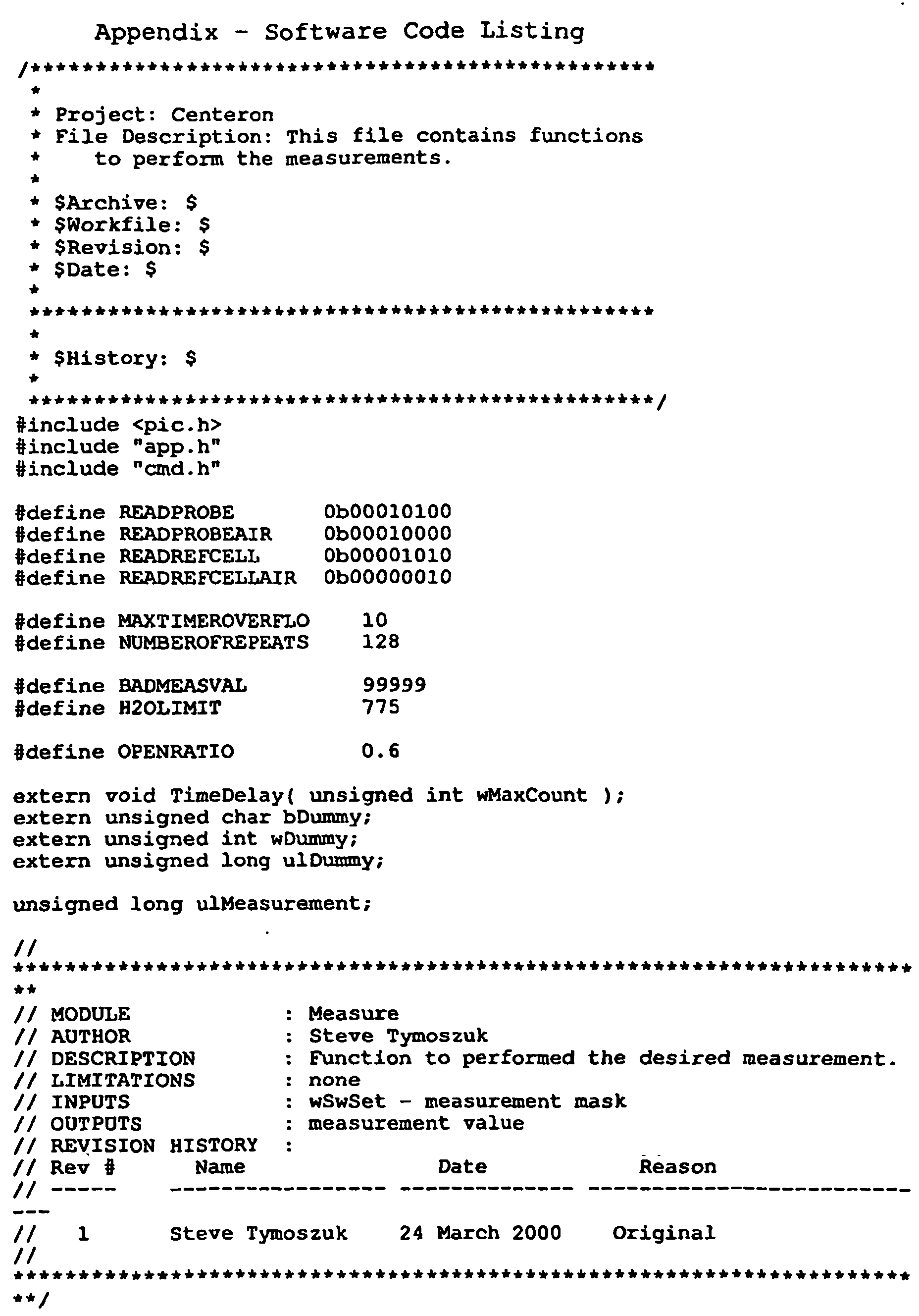
- this modified level equation (Eq. 3) provides a temperature correction term in real time. Exemplary software used to implement this function is included in the Appendix attached hereto.
- microprocessor 200 may function as a 'slave' processor coupled by interface port 180 (Fig. 3) to port 182 of a 'master' microprocessor 210 (Fig. 4).
- EEPROM 100 is coupled directly to microprocessor 210.
- master microprocessor 210 may provide the slave processor 200 with power, a clock pulse, and access to the EEPROM 100.
- Master microprocessor 210 may also control a wireless module (e.g., an ASIC) 220 configured to enable the probe 10 to operate wirelessly by RF or other wireless means.
- a wireless module e.g., an ASIC
- the present invention may be configured without dual Master/Slave processors and/or without wireless capability.
- a single processor 200 may be used, having the EEPROM 100 or other memory storage device coupled directly thereto, with or without wireless module 220.
Landscapes
- Physics & Mathematics (AREA)
- Power Engineering (AREA)
- Engineering & Computer Science (AREA)
- General Physics & Mathematics (AREA)
- Thermal Sciences (AREA)
- Fluid Mechanics (AREA)
- Electromagnetism (AREA)
- Measurement Of Resistance Or Impedance (AREA)
- Measurement Of Length, Angles, Or The Like Using Electric Or Magnetic Means (AREA)
- Measurement Of Levels Of Liquids Or Fluent Solid Materials (AREA)
- Arrangements For Transmission Of Measured Signals (AREA)
- Measuring Leads Or Probes (AREA)
- Investigating Or Analyzing Materials By The Use Of Electric Means (AREA)
Abstract
Description
- This invention relates to capacitance measurement probes, and more particularly, to a capacitance probe and operational circuitry therefor.
- Capacitance probes are often used to measure the level of a material in a tank or other compartment. As the material rises in the compartment, it replaces the air between two electrodes or conductors. If the material has a higher dielectric constant than air, the total capacitance of the system is increased as the compartment is filled. This increase in capacitance provides an indication of the amount of material in the compartment.
- In order for capacitance probes to operate in this setting, a pair of conductors must be spaced such that the material to be measured may fill the space therebetween. If the probe is to be inserted into conductive materials, then it must also incorporate some method of electrically insulating the conductors from one another.
- One capacitive apparatus, shown in U.S. Patent No. 3,774,238 to Hardway, uses two long tubes or
rods plastic insulators 28. - Another type of capacitance probe, shown in U.S. Patent No. 5,397,995 to Anderson, includes an outer conductor and a spaced inner conductor. The space between conductors insulates the conductors from one another and allows the material to be measured to fill the space.
- US-A-6 016 697 discloses a capacitive level detection system including an elongated capacitive probe positioned vertically within the container so that a lower portion of the probe is in liquid and an upper portion of the probe extends above the surface of the liquid. A capacitive liquid reference sensor is proximate the lower end of the probe, and a capacitive gas reference sensor is proximate the upper end of the probe. A controller drives each of the sensors with an electrical signal and reeds a resultant value corresponding to the capacitance of each of the sensors.
- DE-A-4329571 discloses a capacitive AC inclination sensor for determining level of lubricating dielectric liquid of vehicle transmission which divides capacitor into two pairs of electrodes spaced by gaps in which liquid is located, which gaps communicate by principle of communication tube.
- US-A-4 383 444 discloses a level measuring system based upon capacitance to current conversion provided with equipment for compensating for variations in dielectric constant in a measured liquid. A reference probe is located entirely within the liquid to be measured. The measurement probe responds both to changes in dielectric constant and variations in liquid level. A differential output from the reference probe and the measurement probe effectuates compensation for variations in the dielectric constant in the material measured. A control unit at the output provides means for automatic calibration through a microprocessor.
- A drawback of known capacitance probes is their susceptibility to inaccuracies due to capacitances, commonly known as 'parasitic capacitances', that exist between various components of the capacitance measurement circuit, including the probe itself. Moreover, these parasitic capacitances are often variable, being influenced by ambient temperature and/or humidity. Thus, a need exists for an improved capacitance measurement probe and circuitry therefor.
- According to an embodiment of this invention, a capacitance level measurement circuit comprises a drive circuit including a power port couplable to a constant-current source, a detector port couplable to a threshold detector, a probe port couplable to a probe capacitor, a reference port couplable to a reference capacitor, a plurality of switches being actuatable to alternately couple said power port to said probe port and to said reference port; said drive circuit being configured to alternately generate a signal of linear ramp waveform having a slope that is proportional to the magnitude of capacitance of a probe capacitor and reference capacitor coupled to said probe port and to said reference port; wherein parasitic capacitance between the reference capacitor and the probe capacitor is substantially eliminated by maintaining voltage across said reference capacitor at the same level as that across said probe capacitor during measurement of capacitance level.
- In a variation, the present invention may include a capacitance probe including this capacitance level measurement circuit.
- In another aspect, the present invention includes a method of determining the capacitance of a level measurements capacitance probe. The method includes providing a selection/shield drive circuit, coupling a constant-current source to the selection/shield drive circuit, coupling a probe capacitor to the selection/drive circuit, coupling a reference capacitor to the selection/drive circuit, and providing the selection/drive circuit with a plurality of switches being actuatable to alternately couple the constant-current source to the probe capacitor and to the reference capacitor. The method also includes configuring the selection/shield drive circuit to alternately generate a signal of linear ramp waveform having a slope that is proportional to the magnitude of capacitance of a probe capacitor and reference capacitor coupled to said probe port and to said reference port, and actuating the switches to alternately couple the constant-current source to the probe capacitor and to the reference capacitor. The selection/shield drive circuit is used to alternately generate a signal of linear ramp waveform having a slope that is proportional to the magnitude of capacitance of a probe capacitor and reference capacitor. A voltage differential of substantially zero volts is maintained between the reference capacitor and the probe capacitor during said use of the selection/shield drive circuit.
- The above and other features and advantages of this invention will be more readily apparent from a reading of the following detailed description of various aspects of the invention taken in conjunction with the accompanying drawings, in which:
- Fig. 1 is a schematic representation of a capacitance probe of the present invention;
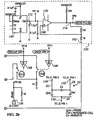
- Fig. 2A is a schematic representation of measurement circuitry of the present invention, useful in operating the capacitance probe of Fig. 1;
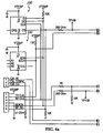
- Fig. 2B is a schematic representation of the electrical wiring of the capacitance probe of Fig. 1;
- Fig. 3 is a schematic representation of a processor used to operate the circuitry of Fig. 2A; and
- Fig. 4 is a schematic representation of additional and/or optional componentry coupled to the circuitry of Figs. 2A and 3.
-
- Referring to the figures set forth in the accompanying Drawings, the illustrative embodiments of the present invention will be described in detail hereinbelow. For clarity of exposition, like features shown in the accompanying Drawings shall be indicated with like reference numerals and similar features as shown in alternate embodiments in the Drawings shall be indicated with similar reference numerals.
- As shown in Figs. 1 & 2A, the subject invention includes a
measurement circuit 22 that may be used in combination with acapacitance probe 10 to measure the level of amaterial 12 in acompartment 14.Probe 10 generally includes a probe capacitor 21 (to measure the material level), and a reference capacitor (cell) 44 used to calibrate theprobe capacitor 21 for aparticular material 12 being measured. Themeasurement circuit 22 actively compensates for parasitic capacitances that typically exist between theprobe capacitor 21 and thereference cell 44.Circuit 22 accomplishes this functionality by supplying a constant current to theprobe capacitor 21 upon initiation of measurement. This constant current generates a voltage across thecapacitor 21 that is a linear ramp waveform having a slope that is proportional to the magnitude of the capacitance. A timer measures the time elapsed ("t") between the initiation of measurement and the time at which the voltage waveform reaches a predetermined level (e.g., 2 volts). This time value "t" is proportional to the value of the capacitance ofprobe capacitor 21. This parasitic capacitance (i.e., between thecapacitor 21 and cell 44) is actively eliminated by maintaining voltage acrossreference cell 44 at the same level as that acrosscapacitor 21 during the measurement cycle. Maintaining these nominally identical voltages substantially eliminates any voltage difference betweencapacitor 21 andcell 44 to nominally eliminate this parasitic capacitance. A similar sequence of events is effected for measurement ofreference cell 44. In this manner, embodiments of the present invention enable relatively accurate measurements of the capacitances ofprobe capacitor 21 andreference cell 44. - Referring now to Figs. 1-4, embodiments of the present invention will be described in greater detail. As shown in Fig. 1. the subject invention includes a
capacitance probe 10 for use in measuring the level of (i.e., depth of insertion of theprobe 10 within) amaterial 12 in acompartment 14.Probe 10 may be of the type set forth in U.S. Patent Application Ser. No. 09/696,329, entitled Low Cost Capacitance Probe, filed on October 24, 2000. In one particular setting,probe 10 has been found to be advantageous in measuring levels of fuel in fuel tanks. - As shown,
probe 10 forms aprobe capacitor 21 exhibiting a capacitance indicated as Cprobe in Fig. 1. Asmaterial 12 rises in a compartment (e.g., tank) 14, it passes into aspace 16 between two electrodes orconductors space 16 throughopenings 25 inouter conductor 20 asmaterial 12 rises intospace 16. Ifmaterial 12 has a higher dielectric constant than air, then the capacitance Cprobe of probe capacitor 21 (i.e., the capacitance betweenconductors 18, 20), is increased ascompartment 16 is filled. This increase in capacitance provides an indication of the amount (i.e., level) ofmaterial 12 incompartment 14. - As also shown,
capacitance probe 10 may include a reference cell (i.e., capacitor) 44 located at adistal end 46 of, and concentrically with,inner conductor 18.Reference cell 44 functions as a relatively small capacitor of known size allowing automatic calibration for the dielectric of theparticular material 12 incompartment 14.Cell 44 thus nominally eliminates the need to calibrate a measurement in the field and allows the system, i.e.,probe 10 andcircuitry 22, to conveniently compensate formaterials 12 of various dielectrics. -
Reference cell 44 includes afirst reference conductor 48 attached using a non-conducting stand-off 50 todistal end 46 ofinner conductor 18. Bothconductor 48 ofreference cell 44, andconductor 18 ofcapacitor 21, are electrically connected tocircuitry 22 by an electrical conductor (e.g., wire) 56 that runs nominally through the center ofinner conductor 18. - In operation,
capacitance probe 10 is inserted at least partly within acompartment 14 having a material 12 therein. Asmaterial 12 fromcompartment 14 entersspace 16 betweeninner conductor 18 andouter conductor 20, the presence ofmaterial 12 serves to alter the electrical field between inner andouter conductors Circuitry 22 measures the capacitance betweenconductors material 12 withinopening 16. Componentry and operation ofcircuitry 22 will be discussed in greater detail hereinbelow. Sincereference cell 44 is completely submerged withinmaterial 12, its capacitance Cref provides a value for a known level (height) ofmaterial 12. The twocapacitors probe 10 may thus be used as variable capacitors to measure material level intank 14. - For example,
reference cell 44 may have a predetermined (axial)length 45, such as 1 to 2 inches (about 2.5 to 5 cm).Probe capacitor 21 may be of any desiredlength 23 representing the range of levels capable of being measured. For many fuel tank applications, (axial)length 23 typically ranges from about 36 to 93 inches (about 91.4 to 236.2 cm). Thecircuitry 22 measures Cprobe and Cref in air and stores these values in memory 100 (e.g., nonvolatile memory of an EEPROM device as shown in Fig. 4). When theprobe 10 is immersed influid 12 with a dielectric different than air, the capacitance Cref of thereference cell 44 changes, as does the capacitance Cprobe of theprobe capacitor 21. This change of capacitance per unit length is measured by thecircuit 22 and the level may be computed by microprocessor 200 (Fig. 3) using the following Equation (1):Equation 1 theoretically generates the desired result because thereference cell 44 has the same radial dimensions as theprobe capacitor 21, thereference cell 44 and thecapacitor 21 are both immersed in the same type offluid 12, and their capacitance change per unit length is nominally identical. The constant Const in theabove Equation 1 corresponds to the length 45 (which in this example is 2 inches). Theprobe 10 is auto-calibrating because the dielectric of the fluid 12 falls out of the level equation Eq. 1, (i.e., because Eq. 1 is ratiometric). As such, the level measurement is independent of the dielectric of the fluid, so it may be used in fluids of many types without further calibration. - A difficulty associated with this configuration is that
wire 56 extending from thereference cell 44 to theelectronics 22 adds a variable, temperature dependent parasitic capacitance shown as Cparasitic in Figs. 1 and 2. This parasitic capacitance also varies as the level offluid 12 changes. This capacitance may thus generate a relatively large error since level equation Eq. 1 does not take this parasitic term into consideration. Thecircuitry 22 of the present invention advantageously serves to eliminate this potential error. -
Circuitry 22 will now be described in greater detail with reference to Figs. 2A-2B.Circuitry 22 includes acurrent source 110, a selection/shield drive portion 120, and athreshold detector 130. As shown in Fig. 2B,conductors terminals drive portion 120.Shield 20 ofprobe 10 is connected toterminal 136 ofdrive portion 120. - Referring now to Fig. 2A in particular, specific componentry of
circuitry 22 is described along with the following functional description thereof. The skilled artisan will recognize that various componentry described herein, such as op-amps and voltage references, typically require power supplies which, according to common practice, may not be explicitly shown in the Figures. In the particular embodiment shown and described, the skilled artisan should recognize that such componentry may be powered by any suitable power supply, such as, for example, an analog 5.0 volt power supply that may be referred to in the Figs. as 'VANALOG'. - As shown,
current source 110 may be a high output impedance current source capable of delivering a constant current of 60 nanoamperes (nA) to driveportion 120, throughoutput pin 136. In the particular embodiment shown,current source 110 includes an Operational Amplifier (Op-Amp) 138, and avoltage reference 140 that produces 2.0 volts atpin 142 relative to pin 144.Current source 110 also includes capacitors C52, C47, resistors R16, R24, and a capacitor C37. Resistors R24 and R16 serve to divide the reference voltage (2.0 volts) down to approximately 0.6 volts, which appears across resistor R22. In the particular embodiment shown, resistor R22 has a resistance of nominally 10 MegOhm (M). The 0.6 volts across the 10M resistor generates a current atoutput 136 of nominally 60nA. -
Current source 110 may be selectively applied to either theprobe capacitor 21 or thereference cell 44, using analog switches 111-116 ofdrive 120, as discussed hereinbelow. By sequencing these switches, the 60 nA constant current may be respectively applied toconnector pin 132,pin 134, or ground. - The sequence of closures of switches 111-116 is controlled by microcontroller 200 (Fig. 3), which is coupled by
output port 151 thereof to control inputs on each analog switch 111-116. These control inputs are respectively labeled PROBE SW, REFCELL SW, REFCAP SW, DISCH SW, DSR SW, and DSP SW, and are each coupled to aswitch actuator 148.Switch actuators 148 operate in a conventional manner to alternately open and close the particular switch 111-116 connected thereto, in response to signals from themicrocontroller 200. - At the beginning of the measurement sequence (also referred to a 'reset' state) switches 111, 112, 113, and 114 are closed and switches 115 and 116 are open. This provides a path to ground through resistor R18 for the 60nA
current source 110, and also serves to groundpins probe capacitor 21 and reference cell 44 (Fig. 1). In this state the voltage atpin 154 of op-amp 138 is nominally (within the compliance of the op-amp 138) at zero volts. Since, in the particular embodiment shown, op-amp 138 is a single supply device, the voltage is within about 20mV of ground. This placespin 144 ofvoltage reference 140 nominally at ground. (As will be discussed in greater detail hereinbelow, sincepin 154 follows the voltage atoutput 136, the voltage atpin 144 also may increase during measurement ofprobe capacitor 21.Reference 140 similarly increases the voltage at itspin 142 to maintain the 2.0 volt differential betweenpins - In this 'reset' state, the current supplied by
source 110 flows to ground through R18 sinceswitches 111 thru 114 are closed. The probe measurement sequence may now begin with themicrocontroller 200closing switches switches amp 152, which is coupled to switch 115 atpin 156 thereof, is configured as a voltage follower so that the voltage at thepin 156 is, within the offset voltage of the op-amp 152, nominally the same as the voltage atpin 154 of op-amp 138. Since op-amp 138 is also configured as a voltage follower, the voltage atpin 154 of op-amp 138 is nominally the same as the voltage atoutput 136. This loop forces the voltage atpin 154 of op-amp 152 to follow the voltage atoutput 136. Thus, in this 'probe measurement' state (i.e., withswitches output 136 through resistor R21 into theprobe capacitor 21 connected atpin 134. - This current flow forces the voltage across the probe capacitor 21 (e.g., between
pin 134 and pin 136) to linearly increase. The closure ofswitch 116 serves to maintain the voltage across the reference cell 44 (connected at pin 132) at the same level as the voltage across the probe capacitor 21 (as this probe capacitor voltage increases). Moreover, this voltage level is maintained incell 44 while current required to charge thereference cell 44 is supplied by op-amp 152 (i.e., atpin 156 thereof) rather than the 60nAcurrent source 110. Advantageously, this functionality effectively maintains the voltage across Cparasitic (i.e., acrossconductors probe capacitor 21 linearly increases (i.e., during the 'ramping period'). This active nulling of the voltage across Cparasitic effectively prevents any current from (i.e., generates a current of zero nA) flowing through Cparasitic so that nominally all of the 60nA current flows into theprobe capacitor 21. Closure ofswitch 113 also applies the voltage atpin 156 of op-amp 152 to the grounded side ofreset switch 114 to similarly null any parasitic capacitance generated byswitch 114 whileswitch 114 is open. - Since
pin 136 is grounded, the increase in voltage across theprobe capacitor 21 generates an increase in the voltage atpin 160 of op-amp 152 (and pin 144 ofreference 140 connected thereto). As mentioned hereinabove, sincereference 140 generates a constant 2.0 volt differential betweenpins pin 144 will result in a similar voltage increase atpin 142. This increasing output serves to maintain the current flow atpin 136 at the aforementioned 60 nA during this 'ramping' or probe measurement period. - The voltage across the probe capacitor 21 (e.g., as taken at pin 160) is fed to input
pin 162 ofthreshold detector 130. This voltage is fed to inputpin 168 of acomparator 170. In the particular embodiment shown,comparator 170 includes an op-amp similar to op-amps comparator 170 compares the probe voltage atpin 168 to the (e.g., 2.0 volt) output atpin 172 of a reference source 140'. (Reference source 140 is substantially similar toreference source 140 described hereinabove with respect tocurrent source 110.) Resistors R28 and R29 may be used to provide a small amount of positive feedback around the threshold detector to prevent false triggering due to noise. When the probe voltage atpin 168 reaches 2.0 volts (i.e., the voltage atpin 168 becomes equal to the voltage at 172), the comparator generates a signal atoutput 174 of the comparator (e.g.,output 174 switches 'high'.) This signal, sometimes referred to herein as 'MEAS PULSE', is input to a timer (e.g., a 16 bit timer) 178 of the microcontroller 200 (Fig. 3).Timer 178 measures the time difference "t" between the closure ofswitch 111 and receipt of the MEAS PULSE signal. Using this timing information, themicrocontroller 200 may compute the capacitance of the probe from the following Equation (2a): - The closure of
switch 113 during the probe measurement process nulls out parasitic capacitance of thereset switch 114, which as discussed hereinabove, is used to ground the 60 nA current during the 'reset' state. Since, as discussed, the current into theprobe capacitor 21 is constant and the time this current flows into thecapacitor 21 is measured, the resolution of measurement is constant, regardless of the size of theprobe capacitor 21. - The capacitance Cref of
reference cell 44 is measured in a manner that is substantially similar to measuring Cprobe as discussed hereinbove, excepting thatswitches current source 110 is supplied to pin 132 for thereference cell 44, rather than to pin 134 for theprobe capacitor 21. - Due to the sensitive nature of the
measurement circuitry 22, relatively large changes in ambient temperature (and humidity) may generate measurement errors. These errors generally result from temperature-induced offset voltage drifts in the op-amps microcontroller 200 may be provided with computer readable program code (software) that measures the parasitic board capacitances at calibration and stores these values (e.g., inEEPROM 100 of Fig. 4). - These parasitic board measurements are performed in substantially the same manner as a probe measurement or reference cell measurement with the following exception. During a parasitic board capacitance measurement, the switches 111-116 are configured as stated hereinabove with respect to measurement of Cprobe, except
switch 111 is open. This forces the 60nA current to flow into the the probe measurement circuitry (without flowing into the probe capacitor 21), to allow the parasitic board capacitance associated with the probe measurement circuitry to be measured as a function of time and temperature. Similarly, the parasitic capacitance associated with the reference cell circuitry is measured as stated hereinabove with respect to measurement of Cref, exceptswitch 112 is open. These runtime values (Cprobecal and Crefcal in Equation 3) are affected by temperature and humidity and they may be measured as the instrument operates in order to compensate for changes therein. During the measurement cycle, these calibration values, e.g., 'Cprobecal' and 'Crefcal', may be retrieved (e.g., from the EEPROM 100) and used to modify the above-referenced level equation (Eq. 1) to produce the following enhanced level equation (Eq. 3): - In the particular embodiment shown in Figs. 3 and 4,
microprocessor 200 may function as a 'slave' processor coupled by interface port 180 (Fig. 3) toport 182 of a 'master' microprocessor 210 (Fig. 4). As also shown,EEPROM 100 is coupled directly tomicroprocessor 210. In this configuration,master microprocessor 210 may provide theslave processor 200 with power, a clock pulse, and access to theEEPROM 100.Master microprocessor 210 may also control a wireless module (e.g., an ASIC) 220 configured to enable theprobe 10 to operate wirelessly by RF or other wireless means. The skilled artisan will recognize that in alternate embodiments, the present invention may be configured without dual Master/Slave processors and/or without wireless capability. For example, asingle processor 200 may be used, having theEEPROM 100 or other memory storage device coupled directly thereto, with or withoutwireless module 220. - In the preceding specification, the invention has been described with reference to specific exemplary embodiments thereof. It will be evident that various modifications and changes may be made thereunto without departing from the scope of the invention as set forth in the claims that follow. The specification and drawings are accordingly to be regarded in an illustrative rather than restrictive sense.


- Having thus described the invention, what is claimed is:
Claims (17)
- A capacitance level measurement circuit (28) comprising:wherein parasitic capacitance between the reference capacitor (44) and the probe capacitor (21) is substantially eliminated by maintaining voltage across said reference capacitor (44) at the same level as that across said probe capacitor (21) during level measurements.a drive circuit including:a power port (136) couplable to a constant-current source (110);a detector port (162) couplable to a threshold detector (130);a probe port (134) couplable to a probe capacitor (21);a reference port (132) couplable to a reference capacitor (44);a plurality of switches (111,112,113,114) being actuatable to alternately couple said power port (136) to said probe port (134) and to said reference port (132);said drive circuit being configured to alternately generate a signal of linear ramp waveform having a slope that is proportional to the magnitude of capacitance of a probe capacitor (21) and reference capacitor (44) coupled to said probe port (134) and to said reference port (132);
- The circuit of claim 1, comprising a constant-current source (110) coupled to said power port (136).
- The circuit of claim 1, comprising:a probe capacitor (21) coupled to said probe port (134); and a reference capacitor (44) coupled to said reference port (132).
- The circuit of claim 1, being configured to maintain a voltage differential of substantially zero volts between the reference capacitor and the probe capacitor.
- The circuit of claim 1, further comprising a threshold detector coupled to said detector port, said threshold detector being configured to indicate when the linear ramp waveform reaches a threshold.
- The circuit of claim 5, wherein the signal comprises a linear ramp voltage waveform in which the voltage varies linearly therealong, and said threshold detector is configured to indicate when the signal reaches a threshold voltage.
- The circuit of claim 6, further comprising a timer to measure time elapsed between coupling said constant-current source to one of the probe and reference capacitors, and the signal reaching the threshold.
- The circuit of claim 7, comprising a microprocessor configured to actuate said switches and to measure said time elapsed.
- The circuit of claim 8, wherein said microprocessor is configured to calculate a level of material into which the probe capacitor is immersed.
- The circuit of claim 9, wherein said microprocessor uses said magnitude of capacitance of the probe.capacitor and reference capacitor to calculate the level of material.
- The circuit of claim 10, wherein said microprocessor implements the equation:
- The circuit of claim 10, comprising computer readable program code configured to compensate for parasitic board capacitances.
- The circuit of claim 12, wherein said computer readable program code comprises:computer readable program code to determine a value of the parasitic board capacitances;computer readable program code to store said value;computer readable program code to retrieve said value during a measurement cycle; andcomputer readable program code to incorporate said value to calculate the level of material.
- The circuit of claim 12, wherein said computer readable program code implements the equation:
- A capacitance probe comprising the capacitance level measurement circuit of claim 1.
- The probe of claim 15, comprising:wherein said circuit is configured to maintain a voltage differential of substantially zero volts between the reference capacitor and the probe capacitor to substantially eliminate parasitic capacitance therebetween.a constant-current source coupled to said power port; a probe capacitor coupled to said probe port;a reference capacitor coupled to said reference port;a threshold detector coupled to said detector port, said threshold detector being configured to indicate when the linear ramp waveform reaches a threshold;
- A method of determining the capacitance of a level measurement capacitance probe, said method comprising:providing a drive circuit;coupling a constant-current source to the drive circuit;coupling a probe capacitor to the selection/drive circuit;coupling a reference capacitor to the selection/drive circuit;providing the selection/drive circuit with a plurality of switches being actuatable to alternately couple the constant-current source to the probe capacitor and to the reference capacitor;configuring the drive circuit to alternately generate a signal of linear ramp waveform having a slope that is proportional to the magnitude of capacitance of a probe capacitor and reference capacitor coupled to said probe port and to said reference port;actuating the switches to alternately couple the constant-current source to the probe capacitor and to the reference capacitor; andusing the drive circuit to alternately generate a signal of linear ramp waveform having a slope that is proportional to the magnitude of capacitance of a probe capacitor and reference capacitor; andmaintaining a voltage differential of substantially zero volts between the reference capacitor and the probe capacitor during said use of the drive circuit.
Applications Claiming Priority (3)
| Application Number | Priority Date | Filing Date | Title |
|---|---|---|---|
| US19719500P | 2000-04-14 | 2000-04-14 | |
| US197195P | 2000-04-14 | ||
| PCT/US2001/012145 WO2001079789A2 (en) | 2000-04-14 | 2001-04-13 | Capacitance level measurement circuit and system |
Publications (2)
| Publication Number | Publication Date |
|---|---|
| EP1274972A2 EP1274972A2 (en) | 2003-01-15 |
| EP1274972B1 true EP1274972B1 (en) | 2005-07-06 |
Family
ID=22728422
Family Applications (1)
| Application Number | Title | Priority Date | Filing Date |
|---|---|---|---|
| EP01932553A Expired - Lifetime EP1274972B1 (en) | 2000-04-14 | 2001-04-13 | Capacitance level measurement circuit and system |
Country Status (7)
| Country | Link |
|---|---|
| US (1) | US6529017B2 (en) |
| EP (1) | EP1274972B1 (en) |
| AT (1) | ATE299267T1 (en) |
| AU (2) | AU2001259069B2 (en) |
| DE (1) | DE60111840T2 (en) |
| ES (1) | ES2245362T3 (en) |
| WO (1) | WO2001079789A2 (en) |
Families Citing this family (35)
| Publication number | Priority date | Publication date | Assignee | Title |
|---|---|---|---|---|
| US6825765B2 (en) * | 1998-12-30 | 2004-11-30 | Automotive Systems Laboratory, Inc. | Occupant detection system |
| US8784335B2 (en) * | 2002-04-19 | 2014-07-22 | Sanofi-Aventis Deutschland Gmbh | Body fluid sampling device with a capacitive sensor |
| US6951549B1 (en) * | 2002-09-30 | 2005-10-04 | Advanced Cardiovascular Systems, Inc. | Systems and methods for detecting tissue contact and needle penetration depth |
| US6857313B2 (en) | 2003-03-31 | 2005-02-22 | Rochester Gauges, Inc. | Self-calibrating capacitance gauge |
| US7114391B2 (en) | 2003-12-26 | 2006-10-03 | Ngk Spark Plug Co., Ltd. | Liquid level detection apparatus |
| US7293578B2 (en) | 2004-01-22 | 2007-11-13 | Rochester Gauges, Inc. | Gauge assembly having a stop fill device |
| US7726334B2 (en) | 2004-01-22 | 2010-06-01 | Rochester Gauges, Inc. | Service valve assembly having a stop-fill device and remote liquid level indicator |
| US7921873B2 (en) | 2004-01-22 | 2011-04-12 | Rochester Gauges, Inc. | Service valve assembly having a stop-fill device and a liquid level indicating dial |
| FR2865921B1 (en) * | 2004-02-11 | 2007-06-01 | Spinevision | EXPLORATION DEVICE FOR TRACKING THE PENETRATION OF AN INSTRUMENT IN AN ANATOMICAL STRUCTURE |
| PL1657533T3 (en) * | 2004-11-15 | 2008-06-30 | Siem Srl | Level sensor extracting its operating power from an indicating instrument |
| EP1677084A1 (en) | 2004-12-22 | 2006-07-05 | Roxer Industries S.A. | LIquid level sensor and method of estimation |
| WO2006133357A2 (en) * | 2005-06-08 | 2006-12-14 | Lumenite Control Technology Inc. | Self-calibrating liquid level transmitter |
| USD583693S1 (en) | 2006-03-30 | 2008-12-30 | Rochester Gauges, Inc. | Dial assembly for a gauge |
| PL1862806T3 (en) * | 2006-06-01 | 2018-01-31 | Electrolux Home Products Corp Nv | Method and device for measuring the capacitance of a capacitive component |
| US7690323B2 (en) | 2007-10-31 | 2010-04-06 | Rochester Gauges, Inc. | Gauge head assembly with non-magnetic insert |
| US8059103B2 (en) * | 2007-11-21 | 2011-11-15 | 3M Innovative Properties Company | System and method for determining touch positions based on position-dependent electrical charges |
| US7830157B2 (en) * | 2007-12-28 | 2010-11-09 | 3M Innovative Properties Company | Pulsed capacitance measuring circuits and methods |
| US8183875B2 (en) * | 2008-11-26 | 2012-05-22 | 3M Innovative Properties Company | System and method for determining touch positions based on passively-induced position-dependent electrical charges |
| US8866499B2 (en) * | 2009-08-27 | 2014-10-21 | Analog Devices, Inc. | System and method for measuring capacitance |
| CA2753588C (en) | 2011-09-27 | 2016-01-26 | Westport Power Inc. | Apparatus and method for volume and mass estimation of a multiphase fluid stored at cryogenic temperatures |
| US20130223111A1 (en) * | 2012-02-23 | 2013-08-29 | System General Corporation | Digital control circuit for resonant power converters |
| TWI445971B (en) * | 2012-07-20 | 2014-07-21 | Wistron Corp | Measurement system for signal |
| GB2505190A (en) * | 2012-08-21 | 2014-02-26 | Schrader Electronics Ltd | Level sensing in a vehicle fuel tank using electromagnetic fields |
| US10598650B2 (en) | 2012-08-22 | 2020-03-24 | General Electric Company | System and method for measuring an operative condition of a machine |
| CN102997974B (en) * | 2012-12-24 | 2014-12-10 | 电子科技大学 | Adaptive capacitance liquid level meter |
| CN103353324B (en) * | 2013-06-05 | 2016-10-05 | 王云平 | A kind of self-alignment capacitance level transducer |
| US9476752B2 (en) * | 2014-10-01 | 2016-10-25 | Sealed Air Corporation | Fluid level sensor |
| AU2016228266A1 (en) * | 2015-09-29 | 2017-04-13 | General Electric Company | System and method for measuring an operative condition of a machine |
| TWI553300B (en) * | 2015-12-01 | 2016-10-11 | 財團法人工業技術研究院 | Liquid level sensing device |
| SE1750077A1 (en) * | 2017-01-31 | 2018-08-01 | Styr Och Elinstallationer Vaest Teknik Ab | Serving system and sensor device for pick-and-mix sales |
| ES2773181T3 (en) * | 2017-02-22 | 2020-07-09 | Zodiac Aerotechnics | Condenser fuel probe |
| DE102017127145B4 (en) * | 2017-11-17 | 2021-03-04 | BEDIA Motorentechnik GmbH & Co. KG | Device and method for capacitive measurement of a fill level of a filling medium |
| CN108692791A (en) * | 2018-03-30 | 2018-10-23 | 厦门乐人电子有限公司 | Liquid level detection device and liquid container |
| US10996095B2 (en) | 2018-07-24 | 2021-05-04 | Sensata Technologies, Inc. | Dielectric-constant-insensitive fluid level sensor |
| WO2022149011A1 (en) * | 2021-11-27 | 2022-07-14 | Basiri Salar | Liquid level measurement apparatus |
Family Cites Families (16)
| Publication number | Priority date | Publication date | Assignee | Title |
|---|---|---|---|---|
| US2544685A (en) | 1946-02-20 | 1951-03-13 | Frank H Jackson | Testing device |
| US2929021A (en) | 1957-03-13 | 1960-03-15 | Western Electric Co | Capacitance and breakdown test set for capacitors |
| US2940037A (en) | 1957-12-16 | 1960-06-07 | Lockheed Aircraft Corp | Capacitance meter |
| US3612997A (en) | 1970-02-18 | 1971-10-12 | John Paulkovich | Capacitor apparatus including a reference capacitor for controlling the current flow through a capacitance being measured |
| US3774238A (en) * | 1971-12-09 | 1973-11-20 | Spearhead Inc | Three-terminal capacitive apparatus for remotely responding to a condition or dielectric properties of a material |
| US4383444A (en) * | 1980-04-21 | 1983-05-17 | Robertshaw Controls Company | Microprocessor based capacitance level detection system |
| US4590575A (en) * | 1981-12-15 | 1986-05-20 | Robertshaw Controls Company | Dielectric compensated level control system for use in tanks containing substance |
| US4558274A (en) | 1983-09-14 | 1985-12-10 | Johnson Service Company | Apparatus and method determining the value of a capacitance |
| DE3610166A1 (en) * | 1985-04-03 | 1986-10-09 | Smiths Industries Public Ltd. Co., London | LEVEL MEASURING DEVICE |
| US5045797A (en) * | 1986-10-14 | 1991-09-03 | Drexelbrook Controls, Inc. | Continuous condition sensing system determining liquid level by admittance measurement |
| US5136251A (en) | 1988-09-23 | 1992-08-04 | John Fluke Mfg. Co., Inc. | Capacitance measurement |
| US5073757A (en) | 1988-09-23 | 1991-12-17 | John Fluke Mfg. Co., Inc. | Apparatus for and method of measuring capacitance of a capacitive element |
| US5469354A (en) | 1989-06-14 | 1995-11-21 | Hitachi, Ltd. | Document data processing method and apparatus for document retrieval |
| DE4329571A1 (en) * | 1992-09-02 | 1994-03-03 | Duerrwaechter E Dr Doduco | Capacitive AC inclination sensor for determining level of lubricating dielectric liquid of vehicle transmission - divides capacitor into two pairs of electrodes spaced by gaps in which liq. is located, which gaps communicate by principle of communicating tubes |
| US5576628A (en) * | 1994-09-30 | 1996-11-19 | Telcom Semiconductor, Inc. | Method and apparatus to measure capacitance |
| US6016697A (en) * | 1997-09-09 | 2000-01-25 | American Magnetics, Inc. | Capacitive level sensor and control system |
-
2001
- 2001-04-13 EP EP01932553A patent/EP1274972B1/en not_active Expired - Lifetime
- 2001-04-13 WO PCT/US2001/012145 patent/WO2001079789A2/en not_active Ceased
- 2001-04-13 AT AT01932553T patent/ATE299267T1/en not_active IP Right Cessation
- 2001-04-13 US US09/835,272 patent/US6529017B2/en not_active Expired - Lifetime
- 2001-04-13 DE DE60111840T patent/DE60111840T2/en not_active Expired - Fee Related
- 2001-04-13 AU AU2001259069A patent/AU2001259069B2/en not_active Ceased
- 2001-04-13 AU AU5906901A patent/AU5906901A/en active Pending
- 2001-04-13 ES ES01932553T patent/ES2245362T3/en not_active Expired - Lifetime
Also Published As
| Publication number | Publication date |
|---|---|
| DE60111840T2 (en) | 2006-08-03 |
| WO2001079789A3 (en) | 2002-02-28 |
| WO2001079789A2 (en) | 2001-10-25 |
| DE60111840D1 (en) | 2005-08-11 |
| ATE299267T1 (en) | 2005-07-15 |
| EP1274972A2 (en) | 2003-01-15 |
| AU5906901A (en) | 2001-10-30 |
| US20020008526A1 (en) | 2002-01-24 |
| ES2245362T3 (en) | 2006-01-01 |
| US6529017B2 (en) | 2003-03-04 |
| AU2001259069B2 (en) | 2004-09-30 |
Similar Documents
| Publication | Publication Date | Title |
|---|---|---|
| US6529017B2 (en) | Capacitance level measurement circuit and system | |
| AU2001259069A1 (en) | Capacitance level measurement circuit and system | |
| US4968946A (en) | Apparatus and method for determining resistance and capacitance values | |
| US4399404A (en) | Moisture tester with probe | |
| US3901079A (en) | Two-mode capacitive liquid level sensing system | |
| US7963164B2 (en) | Capacitive sensor assembly for determining level of fluent materials | |
| US4806847A (en) | Dielectric liquid level sensor and method | |
| EP2614340B1 (en) | Capacitive liquid level sensor | |
| US6894502B2 (en) | pH sensor with internal solution ground | |
| US4789946A (en) | System for measuring the level of filling | |
| US4383444A (en) | Microprocessor based capacitance level detection system | |
| US7550979B2 (en) | System and method for measuring conductivity of fluid | |
| US4176553A (en) | Liquid level measuring system | |
| US7472028B2 (en) | Sensor or capacitance measuring with a microprocessor | |
| JPS5895219A (en) | Device for supplying extremely small amount of liquid | |
| US4795967A (en) | Level measuring device for electrically non-conductive liquids | |
| US20200141789A1 (en) | Capacitive measuring method, and filling level measuring device | |
| CA3168409C (en) | Capacitive filling level probe without dead zone | |
| US20200333175A1 (en) | Dual Polarity Mutual Capacitive Liquid Sensing | |
| JP3625788B2 (en) | Sensor | |
| US5860316A (en) | Capacitance probe | |
| US4462250A (en) | Grain moisture meter | |
| US11668595B1 (en) | Fluid level and conductivity sensor for high temperature applications | |
| JP3367168B2 (en) | Level measuring method and level measuring instrument | |
| US3593118A (en) | Apparatus for measuring the electrical conductivity of liquids having dielectric-faced electrodes |
Legal Events
| Date | Code | Title | Description |
|---|---|---|---|
| PUAI | Public reference made under article 153(3) epc to a published international application that has entered the european phase |
Free format text: ORIGINAL CODE: 0009012 |
|
| 17P | Request for examination filed |
Effective date: 20021111 |
|
| AK | Designated contracting states |
Kind code of ref document: A2 Designated state(s): AT BE CH CY DE DK ES FI FR GB GR IE IT LI LU MC NL PT SE TR |
|
| AX | Request for extension of the european patent |
Free format text: AL;LT;LV;MK;RO;SI |
|
| 17Q | First examination report despatched |
Effective date: 20040422 |
|
| 111Z | Information provided on other rights and legal means of execution |
Free format text: ATBECHCYDEDKESFIFRGBGRIEITLILUMCNLPTSETR Effective date: 20040607 |
|
| GRAP | Despatch of communication of intention to grant a patent |
Free format text: ORIGINAL CODE: EPIDOSNIGR1 |
|
| GRAP | Despatch of communication of intention to grant a patent |
Free format text: ORIGINAL CODE: EPIDOSNIGR1 |
|
| GRAS | Grant fee paid |
Free format text: ORIGINAL CODE: EPIDOSNIGR3 |
|
| GRAA | (expected) grant |
Free format text: ORIGINAL CODE: 0009210 |
|
| AK | Designated contracting states |
Kind code of ref document: B1 Designated state(s): AT BE CH CY DE DK ES FI FR GB GR IE IT LI LU MC NL PT SE TR |
|
| PG25 | Lapsed in a contracting state [announced via postgrant information from national office to epo] |
Ref country code: NL Free format text: LAPSE BECAUSE OF FAILURE TO SUBMIT A TRANSLATION OF THE DESCRIPTION OR TO PAY THE FEE WITHIN THE PRESCRIBED TIME-LIMIT Effective date: 20050706 Ref country code: TR Free format text: LAPSE BECAUSE OF FAILURE TO SUBMIT A TRANSLATION OF THE DESCRIPTION OR TO PAY THE FEE WITHIN THE PRESCRIBED TIME-LIMIT Effective date: 20050706 Ref country code: AT Free format text: LAPSE BECAUSE OF FAILURE TO SUBMIT A TRANSLATION OF THE DESCRIPTION OR TO PAY THE FEE WITHIN THE PRESCRIBED TIME-LIMIT Effective date: 20050706 Ref country code: FI Free format text: LAPSE BECAUSE OF FAILURE TO SUBMIT A TRANSLATION OF THE DESCRIPTION OR TO PAY THE FEE WITHIN THE PRESCRIBED TIME-LIMIT Effective date: 20050706 Ref country code: LI Free format text: LAPSE BECAUSE OF FAILURE TO SUBMIT A TRANSLATION OF THE DESCRIPTION OR TO PAY THE FEE WITHIN THE PRESCRIBED TIME-LIMIT Effective date: 20050706 Ref country code: BE Free format text: LAPSE BECAUSE OF FAILURE TO SUBMIT A TRANSLATION OF THE DESCRIPTION OR TO PAY THE FEE WITHIN THE PRESCRIBED TIME-LIMIT Effective date: 20050706 Ref country code: CH Free format text: LAPSE BECAUSE OF FAILURE TO SUBMIT A TRANSLATION OF THE DESCRIPTION OR TO PAY THE FEE WITHIN THE PRESCRIBED TIME-LIMIT Effective date: 20050706 |
|
| REG | Reference to a national code |
Ref country code: GB Ref legal event code: FG4D |
|
| REG | Reference to a national code |
Ref country code: CH Ref legal event code: EP |
|
| REG | Reference to a national code |
Ref country code: IE Ref legal event code: FG4D |
|
| REF | Corresponds to: |
Ref document number: 60111840 Country of ref document: DE Date of ref document: 20050811 Kind code of ref document: P |
|
| PG25 | Lapsed in a contracting state [announced via postgrant information from national office to epo] |
Ref country code: SE Free format text: LAPSE BECAUSE OF FAILURE TO SUBMIT A TRANSLATION OF THE DESCRIPTION OR TO PAY THE FEE WITHIN THE PRESCRIBED TIME-LIMIT Effective date: 20051006 Ref country code: GR Free format text: LAPSE BECAUSE OF FAILURE TO SUBMIT A TRANSLATION OF THE DESCRIPTION OR TO PAY THE FEE WITHIN THE PRESCRIBED TIME-LIMIT Effective date: 20051006 Ref country code: DK Free format text: LAPSE BECAUSE OF FAILURE TO SUBMIT A TRANSLATION OF THE DESCRIPTION OR TO PAY THE FEE WITHIN THE PRESCRIBED TIME-LIMIT Effective date: 20051006 |
|
| PG25 | Lapsed in a contracting state [announced via postgrant information from national office to epo] |
Ref country code: PT Free format text: LAPSE BECAUSE OF FAILURE TO SUBMIT A TRANSLATION OF THE DESCRIPTION OR TO PAY THE FEE WITHIN THE PRESCRIBED TIME-LIMIT Effective date: 20051212 |
|
| REG | Reference to a national code |
Ref country code: GB Ref legal event code: 732E |
|
| REG | Reference to a national code |
Ref country code: ES Ref legal event code: FG2A Ref document number: 2245362 Country of ref document: ES Kind code of ref document: T3 |
|
| NLV1 | Nl: lapsed or annulled due to failure to fulfill the requirements of art. 29p and 29m of the patents act | ||
| REG | Reference to a national code |
Ref country code: CH Ref legal event code: PL |
|
| REG | Reference to a national code |
Ref country code: FR Ref legal event code: CA Ref country code: FR Ref legal event code: TP |
|
| PG25 | Lapsed in a contracting state [announced via postgrant information from national office to epo] |
Ref country code: IE Free format text: LAPSE BECAUSE OF NON-PAYMENT OF DUE FEES Effective date: 20060413 |
|
| ET | Fr: translation filed | ||
| PG25 | Lapsed in a contracting state [announced via postgrant information from national office to epo] |
Ref country code: MC Free format text: LAPSE BECAUSE OF NON-PAYMENT OF DUE FEES Effective date: 20060430 |
|
| REG | Reference to a national code |
Ref country code: ES Ref legal event code: PC2A |
|
| PLBE | No opposition filed within time limit |
Free format text: ORIGINAL CODE: 0009261 |
|
| STAA | Information on the status of an ep patent application or granted ep patent |
Free format text: STATUS: NO OPPOSITION FILED WITHIN TIME LIMIT |
|
| 26N | No opposition filed |
Effective date: 20060407 |
|
| REG | Reference to a national code |
Ref country code: IE Ref legal event code: MM4A |
|
| PG25 | Lapsed in a contracting state [announced via postgrant information from national office to epo] |
Ref country code: LU Free format text: LAPSE BECAUSE OF NON-PAYMENT OF DUE FEES Effective date: 20060413 |
|
| PG25 | Lapsed in a contracting state [announced via postgrant information from national office to epo] |
Ref country code: CY Free format text: LAPSE BECAUSE OF FAILURE TO SUBMIT A TRANSLATION OF THE DESCRIPTION OR TO PAY THE FEE WITHIN THE PRESCRIBED TIME-LIMIT Effective date: 20050706 |
|
| PGFP | Annual fee paid to national office [announced via postgrant information from national office to epo] |
Ref country code: GB Payment date: 20090312 Year of fee payment: 9 |
|
| PGFP | Annual fee paid to national office [announced via postgrant information from national office to epo] |
Ref country code: ES Payment date: 20090420 Year of fee payment: 9 |
|
| PGFP | Annual fee paid to national office [announced via postgrant information from national office to epo] |
Ref country code: DE Payment date: 20090430 Year of fee payment: 9 Ref country code: FR Payment date: 20090406 Year of fee payment: 9 Ref country code: IT Payment date: 20090420 Year of fee payment: 9 |
|
| GBPC | Gb: european patent ceased through non-payment of renewal fee |
Effective date: 20100413 |
|
| REG | Reference to a national code |
Ref country code: FR Ref legal event code: ST Effective date: 20101230 |
|
| PG25 | Lapsed in a contracting state [announced via postgrant information from national office to epo] |
Ref country code: DE Free format text: LAPSE BECAUSE OF NON-PAYMENT OF DUE FEES Effective date: 20101103 |
|
| PG25 | Lapsed in a contracting state [announced via postgrant information from national office to epo] |
Ref country code: IT Free format text: LAPSE BECAUSE OF NON-PAYMENT OF DUE FEES Effective date: 20100413 Ref country code: GB Free format text: LAPSE BECAUSE OF NON-PAYMENT OF DUE FEES Effective date: 20100413 |
|
| REG | Reference to a national code |
Ref country code: ES Ref legal event code: FD2A Effective date: 20110714 |
|
| PG25 | Lapsed in a contracting state [announced via postgrant information from national office to epo] |
Ref country code: ES Free format text: LAPSE BECAUSE OF NON-PAYMENT OF DUE FEES Effective date: 20110704 |
|
| PG25 | Lapsed in a contracting state [announced via postgrant information from national office to epo] |
Ref country code: ES Free format text: LAPSE BECAUSE OF NON-PAYMENT OF DUE FEES Effective date: 20100414 |
|
| PG25 | Lapsed in a contracting state [announced via postgrant information from national office to epo] |
Ref country code: FR Free format text: LAPSE BECAUSE OF NON-PAYMENT OF DUE FEES Effective date: 20100430 |