EP1273966A1 - Black and white photographic material - Google Patents
Black and white photographic material Download PDFInfo
- Publication number
- EP1273966A1 EP1273966A1 EP02012607A EP02012607A EP1273966A1 EP 1273966 A1 EP1273966 A1 EP 1273966A1 EP 02012607 A EP02012607 A EP 02012607A EP 02012607 A EP02012607 A EP 02012607A EP 1273966 A1 EP1273966 A1 EP 1273966A1
- Authority
- EP
- European Patent Office
- Prior art keywords
- polymer
- silver
- layer
- emulsion layer
- gain
- Prior art date
- Legal status (The legal status is an assumption and is not a legal conclusion. Google has not performed a legal analysis and makes no representation as to the accuracy of the status listed.)
- Granted
Links
- 239000000463 material Substances 0.000 title claims abstract description 27
- 239000000839 emulsion Substances 0.000 claims abstract description 34
- 229910052709 silver Inorganic materials 0.000 claims abstract description 31
- 239000004332 silver Substances 0.000 claims abstract description 31
- 229920000642 polymer Polymers 0.000 claims abstract description 25
- BQCADISMDOOEFD-UHFFFAOYSA-N Silver Chemical compound [Ag] BQCADISMDOOEFD-UHFFFAOYSA-N 0.000 claims abstract description 20
- 239000011159 matrix material Substances 0.000 claims abstract description 20
- -1 silver halide Chemical class 0.000 claims abstract description 15
- 230000003287 optical effect Effects 0.000 claims abstract description 10
- 239000011230 binding agent Substances 0.000 claims abstract description 6
- 108010010803 Gelatin Proteins 0.000 claims description 11
- 229920000159 gelatin Polymers 0.000 claims description 11
- 239000008273 gelatin Substances 0.000 claims description 11
- 235000019322 gelatine Nutrition 0.000 claims description 11
- 235000011852 gelatine desserts Nutrition 0.000 claims description 11
- 230000005855 radiation Effects 0.000 claims description 10
- 239000000758 substrate Substances 0.000 claims description 8
- 238000000034 method Methods 0.000 claims description 6
- 150000003926 acrylamides Chemical class 0.000 claims description 3
- 150000001252 acrylic acid derivatives Chemical class 0.000 claims description 3
- 150000002734 metacrylic acid derivatives Chemical class 0.000 claims description 3
- FQPSGWSUVKBHSU-UHFFFAOYSA-N methacrylamide Chemical class CC(=C)C(N)=O FQPSGWSUVKBHSU-UHFFFAOYSA-N 0.000 claims description 3
- 239000000178 monomer Substances 0.000 claims description 3
- 230000001678 irradiating effect Effects 0.000 claims description 2
- 238000006116 polymerization reaction Methods 0.000 claims description 2
- 229920002120 photoresistant polymer Polymers 0.000 description 26
- RYGMFSIKBFXOCR-UHFFFAOYSA-N Copper Chemical compound [Cu] RYGMFSIKBFXOCR-UHFFFAOYSA-N 0.000 description 9
- 238000000576 coating method Methods 0.000 description 9
- 229910052802 copper Inorganic materials 0.000 description 9
- 239000010949 copper Substances 0.000 description 9
- BAPJBEWLBFYGME-UHFFFAOYSA-N Methyl acrylate Chemical compound COC(=O)C=C BAPJBEWLBFYGME-UHFFFAOYSA-N 0.000 description 8
- 239000011248 coating agent Substances 0.000 description 6
- XHZPRMZZQOIPDS-UHFFFAOYSA-N 2-Methyl-2-[(1-oxo-2-propenyl)amino]-1-propanesulfonic acid Chemical compound OS(=O)(=O)CC(C)(C)NC(=O)C=C XHZPRMZZQOIPDS-UHFFFAOYSA-N 0.000 description 5
- 230000000694 effects Effects 0.000 description 5
- 238000004519 manufacturing process Methods 0.000 description 5
- 159000000000 sodium salts Chemical class 0.000 description 5
- IBDVWXAVKPRHCU-UHFFFAOYSA-N 2-(2-methylprop-2-enoyloxy)ethyl 3-oxobutanoate Chemical compound CC(=O)CC(=O)OCCOC(=O)C(C)=C IBDVWXAVKPRHCU-UHFFFAOYSA-N 0.000 description 4
- 229920002799 BoPET Polymers 0.000 description 4
- 239000005041 Mylar™ Substances 0.000 description 4
- 229920001577 copolymer Polymers 0.000 description 4
- 239000000203 mixture Substances 0.000 description 3
- 229920000139 polyethylene terephthalate Polymers 0.000 description 3
- 239000005020 polyethylene terephthalate Substances 0.000 description 3
- 238000000926 separation method Methods 0.000 description 3
- 238000005406 washing Methods 0.000 description 3
- QIGBRXMKCJKVMJ-UHFFFAOYSA-N Hydroquinone Chemical compound OC1=CC=C(O)C=C1 QIGBRXMKCJKVMJ-UHFFFAOYSA-N 0.000 description 2
- CQEYYJKEWSMYFG-UHFFFAOYSA-N butyl acrylate Chemical compound CCCCOC(=O)C=C CQEYYJKEWSMYFG-UHFFFAOYSA-N 0.000 description 2
- 239000000084 colloidal system Substances 0.000 description 2
- 230000003247 decreasing effect Effects 0.000 description 2
- 238000011161 development Methods 0.000 description 2
- 238000001035 drying Methods 0.000 description 2
- 239000004816 latex Substances 0.000 description 2
- 229920000126 latex Polymers 0.000 description 2
- 239000007788 liquid Substances 0.000 description 2
- DZVCFNFOPIZQKX-LTHRDKTGSA-M merocyanine Chemical compound [Na+].O=C1N(CCCC)C(=O)N(CCCC)C(=O)C1=C\C=C\C=C/1N(CCCS([O-])(=O)=O)C2=CC=CC=C2O\1 DZVCFNFOPIZQKX-LTHRDKTGSA-M 0.000 description 2
- 239000002245 particle Substances 0.000 description 2
- 238000004886 process control Methods 0.000 description 2
- 238000012545 processing Methods 0.000 description 2
- 230000001681 protective effect Effects 0.000 description 2
- 238000011160 research Methods 0.000 description 2
- 230000001235 sensitizing effect Effects 0.000 description 2
- 239000007787 solid Substances 0.000 description 2
- 125000006850 spacer group Chemical group 0.000 description 2
- 239000012780 transparent material Substances 0.000 description 2
- VKONPNAILGGMSR-UHFFFAOYSA-N 2-(2-sulfanylidene-3h-1,3-thiazol-4-yl)acetic acid Chemical compound OC(=O)CC1=CSC(=S)N1 VKONPNAILGGMSR-UHFFFAOYSA-N 0.000 description 1
- NNRHCYIFSMPICW-UHFFFAOYSA-N 4-(2-methylprop-2-enoyloxy)-3-oxohexanoic acid Chemical compound CC(=C)C(=O)OC(CC)C(=O)CC(O)=O NNRHCYIFSMPICW-UHFFFAOYSA-N 0.000 description 1
- KANZXCADWNDNHC-UHFFFAOYSA-N Cc1nc2nc(CS)nn2c(O)c1C(O)=O Chemical compound Cc1nc2nc(CS)nn2c(O)c1C(O)=O KANZXCADWNDNHC-UHFFFAOYSA-N 0.000 description 1
- 206010070834 Sensitisation Diseases 0.000 description 1
- NINIDFKCEFEMDL-UHFFFAOYSA-N Sulfur Chemical compound [S] NINIDFKCEFEMDL-UHFFFAOYSA-N 0.000 description 1
- 239000005864 Sulphur Substances 0.000 description 1
- 125000005250 alkyl acrylate group Chemical group 0.000 description 1
- 150000001412 amines Chemical class 0.000 description 1
- 238000013459 approach Methods 0.000 description 1
- CODNYICXDISAEA-UHFFFAOYSA-N bromine monochloride Chemical compound BrCl CODNYICXDISAEA-UHFFFAOYSA-N 0.000 description 1
- 125000003178 carboxy group Chemical group [H]OC(*)=O 0.000 description 1
- 239000005018 casein Substances 0.000 description 1
- BECPQYXYKAMYBN-UHFFFAOYSA-N casein, tech. Chemical compound NCCCCC(C(O)=O)N=C(O)C(CC(O)=O)N=C(O)C(CCC(O)=N)N=C(O)C(CC(C)C)N=C(O)C(CCC(O)=O)N=C(O)C(CC(O)=O)N=C(O)C(CCC(O)=O)N=C(O)C(C(C)O)N=C(O)C(CCC(O)=N)N=C(O)C(CCC(O)=N)N=C(O)C(CCC(O)=N)N=C(O)C(CCC(O)=O)N=C(O)C(CCC(O)=O)N=C(O)C(COP(O)(O)=O)N=C(O)C(CCC(O)=N)N=C(O)C(N)CC1=CC=CC=C1 BECPQYXYKAMYBN-UHFFFAOYSA-N 0.000 description 1
- 235000021240 caseins Nutrition 0.000 description 1
- 239000003795 chemical substances by application Substances 0.000 description 1
- 150000001875 compounds Chemical class 0.000 description 1
- 230000008602 contraction Effects 0.000 description 1
- 239000013078 crystal Substances 0.000 description 1
- 238000005520 cutting process Methods 0.000 description 1
- 238000013461 design Methods 0.000 description 1
- 238000005530 etching Methods 0.000 description 1
- 238000011156 evaluation Methods 0.000 description 1
- 239000007888 film coating Substances 0.000 description 1
- 238000009501 film coating Methods 0.000 description 1
- 239000011521 glass Substances 0.000 description 1
- PCHJSUWPFVWCPO-UHFFFAOYSA-N gold Chemical compound [Au] PCHJSUWPFVWCPO-UHFFFAOYSA-N 0.000 description 1
- 229910052737 gold Inorganic materials 0.000 description 1
- 239000010931 gold Substances 0.000 description 1
- 239000000543 intermediate Substances 0.000 description 1
- 238000005259 measurement Methods 0.000 description 1
- SCWKACOBHZIKDI-UHFFFAOYSA-N n-[3-(5-sulfanylidene-2h-tetrazol-1-yl)phenyl]acetamide Chemical compound CC(=O)NC1=CC=CC(N2C(N=NN2)=S)=C1 SCWKACOBHZIKDI-UHFFFAOYSA-N 0.000 description 1
- 229920000728 polyester Polymers 0.000 description 1
- 229920000036 polyvinylpyrrolidone Polymers 0.000 description 1
- 239000001267 polyvinylpyrrolidone Substances 0.000 description 1
- 235000013855 polyvinylpyrrolidone Nutrition 0.000 description 1
- 238000002360 preparation method Methods 0.000 description 1
- 150000003283 rhodium Chemical class 0.000 description 1
- 238000012216 screening Methods 0.000 description 1
- 230000008313 sensitization Effects 0.000 description 1
- 230000003595 spectral effect Effects 0.000 description 1
- 239000004094 surface-active agent Substances 0.000 description 1
- 238000002834 transmittance Methods 0.000 description 1
- 229920006163 vinyl copolymer Polymers 0.000 description 1
- 229920002554 vinyl polymer Polymers 0.000 description 1
Images


Classifications
-
- G—PHYSICS
- G03—PHOTOGRAPHY; CINEMATOGRAPHY; ANALOGOUS TECHNIQUES USING WAVES OTHER THAN OPTICAL WAVES; ELECTROGRAPHY; HOLOGRAPHY
- G03C—PHOTOSENSITIVE MATERIALS FOR PHOTOGRAPHIC PURPOSES; PHOTOGRAPHIC PROCESSES, e.g. CINE, X-RAY, COLOUR, STEREO-PHOTOGRAPHIC PROCESSES; AUXILIARY PROCESSES IN PHOTOGRAPHY
- G03C1/00—Photosensitive materials
- G03C1/005—Silver halide emulsions; Preparation thereof; Physical treatment thereof; Incorporation of additives therein
- G03C1/04—Silver halide emulsions; Preparation thereof; Physical treatment thereof; Incorporation of additives therein with macromolecular additives; with layer-forming substances
- G03C1/053—Polymers obtained by reactions involving only carbon-to-carbon unsaturated bonds, e.g. vinyl polymers
-
- G—PHYSICS
- G03—PHOTOGRAPHY; CINEMATOGRAPHY; ANALOGOUS TECHNIQUES USING WAVES OTHER THAN OPTICAL WAVES; ELECTROGRAPHY; HOLOGRAPHY
- G03C—PHOTOSENSITIVE MATERIALS FOR PHOTOGRAPHIC PURPOSES; PHOTOGRAPHIC PROCESSES, e.g. CINE, X-RAY, COLOUR, STEREO-PHOTOGRAPHIC PROCESSES; AUXILIARY PROCESSES IN PHOTOGRAPHY
- G03C2200/00—Details
- G03C2200/16—Black-and-white material
-
- G—PHYSICS
- G03—PHOTOGRAPHY; CINEMATOGRAPHY; ANALOGOUS TECHNIQUES USING WAVES OTHER THAN OPTICAL WAVES; ELECTROGRAPHY; HOLOGRAPHY
- G03C—PHOTOSENSITIVE MATERIALS FOR PHOTOGRAPHIC PURPOSES; PHOTOGRAPHIC PROCESSES, e.g. CINE, X-RAY, COLOUR, STEREO-PHOTOGRAPHIC PROCESSES; AUXILIARY PROCESSES IN PHOTOGRAPHY
- G03C2200/00—Details
- G03C2200/47—Polymer
Definitions
- the present invention relates to a black and white photographic material and in particular to a black and white photographic material suitable for use in optical contact copying.
- the invention also relates to a method of manufacturing a printed circuit board using the black and white photographic material.
- Black and white high contrast silver halide materials are used widely as originals for optical contact copying onto other photosensitive materials.
- page separations are exposed by imagesetter onto film which is then copied (exposed) onto printing plates by ultra-violet (UV) contact exposure.
- UV ultra-violet
- the exposed printing plate is then processed to produce an ink-receptive image for printing on a press.
- pages are physically assembled by cutting and pasting images and text from various sources.
- the assembled page may then be copied by camera onto another sheet of film. This process also induces a feature size change before the final copying of this film image onto a printing plate which further exaggerates the size gain.
- FIG. 1 shows an arrangement for exposing an image through a photomask onto the circuit board.
- the photomask comprises a support 1 and an image layer 2 arranged thereon.
- the photomask is positioned immediately adjacent to a copper-clad, resist-covered PCB substrate on a contact-copying frame (not shown).
- a contact-copying frame not shown.
- Incident radiation such as UV light is provided by a source (not shown) within the contact frame and is received by the photomask and transmitted directly to the photoresist layer 4 through openings in the mask.
- the mask is a photographic film and openings in the mask correspond to minimum density regions of the image on the film.
- the transmitted radiation causes a change in the properties of the photoresist e.g. a hardening such that areas exposed to the radiation are physically different from those that have been hidden by the mask layer 2.
- the photoresist is processed to remove it from areas where it is desired to etch away the copper such that the resultant structure has regions of copper exposed and regions concealed by photoresist.
- the exposed areas of the copper are then etched. After etching, the remaining photoresist is removed from the PCB to reveal the track pattern.
- a problem, known as contact gain, that exists with these kind of contact copying processes is that the image feature size on the copy is often slightly different from the feature size on the original mask. In the printing industry this effect is known as "dot gain", a typical measure of which is the % transmittance change of a black area, often a dot, within its total possible area, defined by the screen ruling. Thus if a dot obscuring 50% of the possible area it can occupy grows to 55% (or 45% depending on whether the printing plate is positive or negative working) on the copy, a dot gain of 5% has occurred.
- contact gain can affect the width of features, e.g. tracks or lines, on a PCB and is referred to as "line width gain".
- line width gain a line width gain of 5 ⁇ m would have occurred.
- the regions of the negative-working photoresist 4 that have been exposed to the UV radiation are slightly larger than the corresponding openings in the mask 2 (where the contact gain is defined as the difference in the feature size of the copy from that of the original).
- the amount of contact gain may vary according to the position of any particular image point across the contact copying frame.
- dry film resist is supplied as a roll comprising 3 layers: a carrier layer, a thin transparent support layer and a photoresist layer.
- the carrier layer is normally separated from the other 2 layers when the dry film resist is applied to the circuit board substrate.
- the photoresist support layer for example a 20 ⁇ m thick Mylar TM film (polyethylene terephthalate) or any other UV transparent material, is placed uppermost on the circuit board with the photoresist layer directly on top of the copper.
- MylarTM film separates the photomask and the photoresist.
- a black and white silver halide material for optical contact copying comprising: at least one photographic emulsion layer including a silver-halide-containing matrix in which the matrix includes a polymer and a hydrophilic binder.
- the ratio of the weight of silver in the emulsion layer to the weight of polymer in the emulsion layer per unit area is less than 2.0.
- the hydrophilic binder is gelatin.
- the polymer may be a polymer derived from the polymerization of one or more ethylenically unsaturated monomers.
- the polymer is selected from a group consisting of acrylates, methacrylates, acrylamides and methacrylamides.
- a method of optical contact copying comprising the step of irradiating a substrate onto which a pattern is to be copied with radiation through an optical mask of the pattern, such that regions of the substrate are selectively exposed or hidden from the radiation.
- the mask is formed of a black and white photographic material according to the first aspect of the present invention.
- the amount of contact gain may be controlled by minimising the coated weight of silver consistent with maintaining adequate maximum image density, together with maximising the coated weight of polymer contained in the emulsion layer consistent with high quality manufacturing requirements.
- Figure 2 shows a schematic representation of an example of a desired mask and photoresist arrangement.
- the arrangement of Figure 2 has a mask layer 2 arranged adjacent to a photoresist layer 4.
- the photoresist layer 4 is arranged on a copper image layer 6, which is to form the channels and connections of a PCB.
- Incident radiation such as ultra violet light is received by the mask layer 2 and transmitted as image information directly to the photoresist layer 4 through openings in the mask.
- Properties of the photomask layer 2 are controlled to ensure that the problem of contact gain is overcome.
- the image transferred to the photoresist which will in turn be copied onto the copper image layer 6 corresponds almost exactly to that of the photomask layer 2.
- the problem of contact gain is substantially overcome.
- the film 7 has a base layer 8, an underlayer 10 and a photographic emulsion layer 12 containing silver halide grains 14.
- the base layer 8 may be formed from a polyester (ESTAR ®) support.
- the photographic emulsion layer 12 is formed of a matrix containing the silver halide grains 14.
- the matrix may be as described in Research Disclosure Item 308119, December 1989 published by Kenneth Mason Publications, Emsworth, Hants UK, hereinafter referred to as Research Disclosure.
- a hydrophilic colloid is used in the matrix such as gelatin or gelatin derivative, polyvinylpyrrolidone or casein and includes a polymer.
- Suitable polymers are acrylates, methacrylates, acrylamides and methacrylamides, e.g., alkyl acrylates such as methyl acrylate and butyl acrylate, (methacryloyloxy)-ethylacetoacetate, and the sodium salt of 2-acrylamido-2-methylpropanesulphonic acid.
- Suitable copolymers of the above monomers may be used, e.g., a copolymer of methyl acrylate, the sodium salt of 2-acrylamido-2-methylpropane sulphonic acid and 2-(methacryloyloxy)-ethylacetoacetate (88:5:7 by weight) and/or a copolymer of butyl acrylate, the sodium salt of 2-acrylamido-2-methylpropanesulphonic acid and 2-(methacryloyloxy)-ethylacetoacetate (90:4:6 by weight).
- a blend of two or more of the above polymers or copolymers may be employed.
- the photographic material 7 may also include a supercoat hydrophilic colloid layer 11 which may also contain a vinyl polymer or copolymer located as the last layer of the coating (furthest from the base layer 8).
- FIG. 4 shows a schematic representation of an enlarged cross section through the emulsion layer 12 of a photographic material according to the present invention.
- the emulsion layer 12 contains developed silver metal 18, which forms an image on the material.
- unexposed silver halide grains are removed, leaving a non-image area 20, from the emulsion layer 12 by a fixing agent.
- a contraction occurs in the emulsion layer 12 such that the thickness d 1 of the emulsion layer 12 at a position where silver halide has been removed is less than the thickness d 2 of the emulsion layer 12 at a position where image silver has not been removed.
- the gelatin, polymer and other binders in the emulsion layer of the film together form the carrier matrix for the silver halide crystals.
- the matrix may also include the gelatin, polymer and other components in other layers of the film, such as the underlayer 10 and supercoat (not shown).
- the silver coated weight should be reduced whilst maintaining or increasing the coated weight of the carrier matrix and increasing its total polymer content.
- the ratio of silver to polymer in the emulsion layer is maintained below 2.0.
- the ratio of silver to matrix in the emulsion layer is maintained below 0.95.
- the desired reduction in contact gain may be achieved if the ratio of silver to matrix in all layers of the material is less than 0.45.
- Figure 5 shows an example of a mask and dry film photoresist arrangement. Like the arrangements of Figures 1 and 2, the arrangement has a mask layer 2 and a photoresist layer 4 to receive transmitted radiation through openings in the mask layer 2.
- the photoresist layer 4 is arranged on a copper layer 6, which is to form the tracks and connections of a PCB.
- Dry film resist is supplied as a roll comprising three layers: a carrier layer (not shown), a thin transparent support layer 22 and a photoresist layer 4. The carrier layer is normally separated from the other two layers when the dry film resist is applied to a circuit board substrate having the copper layer 6.
- the photoresist support layer 22 for example a 20 ⁇ m thick Mylar film or any other UV transparent material, is placed uppermost on the PCB with the photoresist layer 4 directly on top of the copper layer 6.
- the Mylar film 22 is now separating the mask layer 2 and the photoresist layer 4. Given that feature sizes in PCBs approach the thickness of the Mylar film 22, this separation represents a significant distance.
- the film coatings prepared consisted of a polyethylene terephthalate (ESTAR TM) support on which was coated an antihalation underlayer, an emulsion layer, and a protective gelatin overcoat.
- ESTAR TM polyethylene terephthalate
- the underlayer consisted of 1.00 g gelatin/sq.m and a blend of latex copolymer of methyl acrylate, the sodium salt of 2-acrylamido-2-methylpropane sulphonic acid and 2-(methacryloyloxy)-ethylacetoacetate (88:5:7 by weight) at 1.00 g/sq.m.
- the protective gelatin overcoat contained surfactants and was coated at a gelatin laydown of 1.465 g/sq.m.
- the layer also contained hydroquinone at 162.2 mg/sq.m and a solid particle safelight protection dye of structure at 140 mg/sq.m.
- the emulsion was coated at silver coverages as described in Table 1 below in a matrix of 1.85 g/sq.m gelatin and a blend of latex copolymer of methyl acrylate, the sodium salt of 2-acrylamido-2-methylpropane sulphonic acid and 2-(methacryloyloxy)-ethylacetoacetate (88:5:7 by weight), (POL "A”), as shown in Table 1 below.
- the layer also contained 6.32 mg/sq.m of a nucleator compound of structure Coating Ag (g/sq.m) POL "A" (g/sq.m) Ag/Total E-pol Ag/Total E-Matrix Ag/Total film matrix A1 3.6 0.550 6.55 1.50 0.61 A2 3.6 1.650 2.18 1.03 0.52 A3 3.0 1.650 1.82 0.86 0.43
- Table 1 above also shows the ratio values for silver:total emulsion layer polymer, silver:total emulsion layer matrix, and silver:total film matrix.
- a line tint pattern was formed on the films as follows.
- the samples were exposed to WRATTENTM 29 filtered light on a sensitometer which had been modified such that a line tint original (40 ⁇ mlines and 40 ⁇ mspaces) was placed over the conventional step tablet.
- the experimental film samples were placed in intimate contact with the tint original before the exposure was made, followed by development in KODAK TM ACCUMAX TM 2000RA developer (diluted 1+2) at 35 deg C for 45 seconds, followed by conventional fixing, washing and drying.
- the resultant line tint patterns were evaluated on an X-RITE TM densitometer in "dot%" mode, such that a patch on each experimental film was found and accurately measured corresponding to a reading of approximately 35%.
- the area was carefully marked, and the films placed on the glass of a KODAK TM CONTACT 2000 TM "2800" contact frame.
- the films were then covered with a sheet of 25 ⁇ mthick polyethylene terephthalate film support to exaggerate the effect of contact gain, and then with a sheet of KODAK TM CONTACT 2000 TM CA4 general purpose contact film.
- UV exposures were made corresponding to either 308 units exposure, or 715 units exposure.
- the CA4 film was processed in KODAK TM RA2000 developer (diluted 1+4) at 35 deg C for 30 seconds, followed by conventional fixing, washing and drying.
- Coatings B1, B2 and B3 were prepared in exactly the same way as coatings A1, A2 and A3, respectively, except that an emulsion with grains 0.185 ⁇ min mean edge length was used, and that spectral sensitization was carried out with 240 mg/Ag mole of trinuclear merocyanine sensitizing dye.
Landscapes
- Chemical & Material Sciences (AREA)
- Chemical Kinetics & Catalysis (AREA)
- Physics & Mathematics (AREA)
- Spectroscopy & Molecular Physics (AREA)
- Engineering & Computer Science (AREA)
- Materials Engineering (AREA)
- General Physics & Mathematics (AREA)
- Photosensitive Polymer And Photoresist Processing (AREA)
- Silver Salt Photography Or Processing Solution Therefor (AREA)
- Exposure And Positioning Against Photoresist Photosensitive Materials (AREA)
Abstract
Description
- The present invention relates to a black and white photographic material and in particular to a black and white photographic material suitable for use in optical contact copying. The invention also relates to a method of manufacturing a printed circuit board using the black and white photographic material.
- Black and white high contrast silver halide materials are used widely as originals for optical contact copying onto other photosensitive materials. For example in the printing industry, page separations are exposed by imagesetter onto film which is then copied (exposed) onto printing plates by ultra-violet (UV) contact exposure. The exposed printing plate is then processed to produce an ink-receptive image for printing on a press. Sometimes, pages are physically assembled by cutting and pasting images and text from various sources. The assembled page may then be copied by camera onto another sheet of film. This process also induces a feature size change before the final copying of this film image onto a printing plate which further exaggerates the size gain.
- Another example of this type of process is the manufacture of printed circuit boards (PCBs) where electronic circuit track layouts are exposed by photoplotter onto film intermediates, called phototools or photomasks. Figure 1 shows an arrangement for exposing an image through a photomask onto the circuit board. The photomask comprises a support 1 and an
image layer 2 arranged thereon. The photomask is positioned immediately adjacent to a copper-clad, resist-covered PCB substrate on a contact-copying frame (not shown). To improve the intimacy of contact it is normal practice to evacuate air from the contact frame. Incident radiation such as UV light is provided by a source (not shown) within the contact frame and is received by the photomask and transmitted directly to thephotoresist layer 4 through openings in the mask. The mask is a photographic film and openings in the mask correspond to minimum density regions of the image on the film. - The transmitted radiation causes a change in the properties of the photoresist e.g. a hardening such that areas exposed to the radiation are physically different from those that have been hidden by the
mask layer 2. After exposure the photoresist is processed to remove it from areas where it is desired to etch away the copper such that the resultant structure has regions of copper exposed and regions concealed by photoresist. The exposed areas of the copper are then etched. After etching, the remaining photoresist is removed from the PCB to reveal the track pattern. - A problem, known as contact gain, that exists with these kind of contact copying processes is that the image feature size on the copy is often slightly different from the feature size on the original mask. In the printing industry this effect is known as "dot gain", a typical measure of which is the % transmittance change of a black area, often a dot, within its total possible area, defined by the screen ruling. Thus if a dot obscuring 50% of the possible area it can occupy grows to 55% (or 45% depending on whether the printing plate is positive or negative working) on the copy, a dot gain of 5% has occurred.
- In the PCB industry, contact gain can affect the width of features, e.g. tracks or lines, on a PCB and is referred to as "line width gain". Thus, if a 100µm line becomes a 105µm line on the photoresist, a line width gain of 5µm would have occurred. In the example shown in Figure 1, the regions of the negative-working
photoresist 4 that have been exposed to the UV radiation are slightly larger than the corresponding openings in the mask 2 (where the contact gain is defined as the difference in the feature size of the copy from that of the original). - In addition to the problem of contact gain, it is known that the amount of contact gain may vary according to the position of any particular image point across the contact copying frame.
- These gain effects make process control more difficult in both examples discussed above. The problem is becoming more severe as the average feature size to be copied is decreasing due to the drive to reduce track sizes on PCBs and to reduce screen ruling or to use stochastic screening techniques with very small dot size in the printing industry.
- A further development in the printed circuit board industry is the use of dry film resist (as shown in Figure 5) rather than the conventional liquid resist where the resist is applied directly to the substrate. As will be explained below, dry film resist is supplied as a roll comprising 3 layers: a carrier layer, a thin transparent support layer and a photoresist layer. The carrier layer is normally separated from the other 2 layers when the dry film resist is applied to the circuit board substrate. The photoresist support layer, for example a 20µm thick Mylar ™ film (polyethylene terephthalate) or any other UV transparent material, is placed uppermost on the circuit board with the photoresist layer directly on top of the copper. Thus the Mylar™ film separates the photomask and the photoresist. Given that feature sizes in printed circuit boards may now be approaching the thickness of the Mylar™ film, this separation represents a significant distance and further degrades the contact performance by increasing the contact gain of the system in comparison to use of liquid resists, where no support layer is necessary.
- It is an aim of the present invention to reduce the amount of contact gain through improved design of the silver halide film original and thus facilitate process control.
- It is also an aim of the present invention to provide a photographic material suitable for use in the manufacture of PCBs or the production of printing plates, adapted such that contact gain is minimised.
- According to a first aspect of the present invention, there is provided a black and white silver halide material for optical contact copying, comprising: at least one photographic emulsion layer including a silver-halide-containing matrix in which the matrix includes a polymer and a hydrophilic binder. The ratio of the weight of silver in the emulsion layer to the weight of polymer in the emulsion layer per unit area is less than 2.0.
- Preferably, the hydrophilic binder is gelatin. The polymer may be a polymer derived from the polymerization of one or more ethylenically unsaturated monomers. Preferably, the polymer is selected from a group consisting of acrylates, methacrylates, acrylamides and methacrylamides.
- According to a second aspect of the present invention, there is provided a method of optical contact copying comprising the step of irradiating a substrate onto which a pattern is to be copied with radiation through an optical mask of the pattern, such that regions of the substrate are selectively exposed or hidden from the radiation. The mask is formed of a black and white photographic material according to the first aspect of the present invention.
- It has been found that the amount of contact gain may be controlled by minimising the coated weight of silver consistent with maintaining adequate maximum image density, together with maximising the coated weight of polymer contained in the emulsion layer consistent with high quality manufacturing requirements.
- Examples of the present invention will now be described in detail with reference to the accompanying drawings, in which:
- Figure 1 shows a schematic representation of an example of a mask and photoresist arrangement demonstrating the problem of contact gain;
- Figure 2 shows a schematic representation of an example of an ideal mask and photoresist arrangement where there is no contact gain;
- Figure 3 shows an example of the layered structure of the photographic film according to an example of the present invention;
- Figure 4 shows an enlarged cross section of the emulsion layer of a photographic material after processing showing both image and non-image areas; and,
- Figure 5 shows an example of a mask and dry film photoresist arrangement.
-
- Figure 2 shows a schematic representation of an example of a desired mask and photoresist arrangement. Like the arrangement of Figure 1, the arrangement of Figure 2 has a
mask layer 2 arranged adjacent to aphotoresist layer 4. In this example, thephotoresist layer 4 is arranged on acopper image layer 6, which is to form the channels and connections of a PCB. Incident radiation such as ultra violet light is received by themask layer 2 and transmitted as image information directly to thephotoresist layer 4 through openings in the mask. - Properties of the
photomask layer 2 are controlled to ensure that the problem of contact gain is overcome. As shown schematically in Figure 2, in the present invention, the image transferred to the photoresist which will in turn be copied onto thecopper image layer 6, corresponds almost exactly to that of thephotomask layer 2. The problem of contact gain is substantially overcome. - Contact gain reduction is achieved by decreasing the relative content of silver in the photographic emulsion layer of the photographic material as will be explained with reference to Figure 3 which shows an example of the layered structure of
photographic film 7 according to an example of the present invention. Thefilm 7 has abase layer 8, anunderlayer 10 and aphotographic emulsion layer 12 containingsilver halide grains 14. Thebase layer 8 may be formed from a polyester (ESTAR ®) support. - In use, an image is exposed onto the
film 7, creating a latent image in thesilver halide grains 14. The exposed material is processed through developer, fixer and washing baths after which it is dried. Thephotographic emulsion layer 12 is formed of a matrix containing thesilver halide grains 14. The matrix may be as described in Research Disclosure Item 308119, December 1989 published by Kenneth Mason Publications, Emsworth, Hants UK, hereinafter referred to as Research Disclosure. A hydrophilic colloid is used in the matrix such as gelatin or gelatin derivative, polyvinylpyrrolidone or casein and includes a polymer. Examples of suitable polymers are acrylates, methacrylates, acrylamides and methacrylamides, e.g., alkyl acrylates such as methyl acrylate and butyl acrylate, (methacryloyloxy)-ethylacetoacetate, and the sodium salt of 2-acrylamido-2-methylpropanesulphonic acid. - Suitable copolymers of the above monomers may be used, e.g., a copolymer of methyl acrylate, the sodium salt of 2-acrylamido-2-methylpropane sulphonic acid and 2-(methacryloyloxy)-ethylacetoacetate (88:5:7 by weight) and/or a copolymer of butyl acrylate, the sodium salt of 2-acrylamido-2-methylpropanesulphonic acid and 2-(methacryloyloxy)-ethylacetoacetate (90:4:6 by weight). A blend of two or more of the above polymers or copolymers may be employed.
- The
photographic material 7 may also include a supercoathydrophilic colloid layer 11 which may also contain a vinyl polymer or copolymer located as the last layer of the coating (furthest from the base layer 8). - Figure 4 shows a schematic representation of an enlarged cross section through the
emulsion layer 12 of a photographic material according to the present invention. Theemulsion layer 12 containsdeveloped silver metal 18, which forms an image on the material. During processing of the photographic material, unexposed silver halide grains are removed, leaving anon-image area 20, from theemulsion layer 12 by a fixing agent. As the unexposed silver halide is removed a contraction occurs in theemulsion layer 12 such that the thickness d1 of theemulsion layer 12 at a position where silver halide has been removed is less than the thickness d2 of theemulsion layer 12 at a position where image silver has not been removed. - To control the amount of contact gain, careful selection of the coated weight of silver relative to the coated weight of the matrix per unit area is required. The gelatin, polymer and other binders in the emulsion layer of the film together form the carrier matrix for the silver halide crystals. The matrix may also include the gelatin, polymer and other components in other layers of the film, such as the
underlayer 10 and supercoat (not shown). To reduce contact gain, the silver coated weight should be reduced whilst maintaining or increasing the coated weight of the carrier matrix and increasing its total polymer content. Preferably, the ratio of silver to polymer in the emulsion layer is maintained below 2.0. Alternatively, the ratio of silver to matrix in the emulsion layer is maintained below 0.95. In a further alternative, the desired reduction in contact gain may be achieved if the ratio of silver to matrix in all layers of the material is less than 0.45. - Figure 5 shows an example of a mask and dry film photoresist arrangement. Like the arrangements of Figures 1 and 2, the arrangement has a
mask layer 2 and aphotoresist layer 4 to receive transmitted radiation through openings in themask layer 2. In this example, thephotoresist layer 4 is arranged on acopper layer 6, which is to form the tracks and connections of a PCB. Dry film resist is supplied as a roll comprising three layers: a carrier layer (not shown), a thintransparent support layer 22 and aphotoresist layer 4. The carrier layer is normally separated from the other two layers when the dry film resist is applied to a circuit board substrate having thecopper layer 6. Thephotoresist support layer 22, for example a 20µm thick Mylar film or any other UV transparent material, is placed uppermost on the PCB with thephotoresist layer 4 directly on top of thecopper layer 6. Thus theMylar film 22 is now separating themask layer 2 and thephotoresist layer 4. Given that feature sizes in PCBs approach the thickness of theMylar film 22, this separation represents a significant distance. - Preparation of the coatings: The film coatings prepared consisted of a polyethylene terephthalate (ESTAR ™) support on which was coated an antihalation underlayer, an emulsion layer, and a protective gelatin overcoat.
- The underlayer consisted of 1.00 g gelatin/sq.m and a blend of latex copolymer of methyl acrylate, the sodium salt of 2-acrylamido-2-methylpropane sulphonic acid and 2-(methacryloyloxy)-ethylacetoacetate (88:5:7 by weight) at 1.00 g/sq.m. The layer also contained an amine booster of structureat 61.5 mg/sq.m and a solid particle antihalation dye of structure
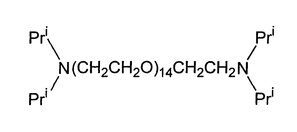 R = CO2H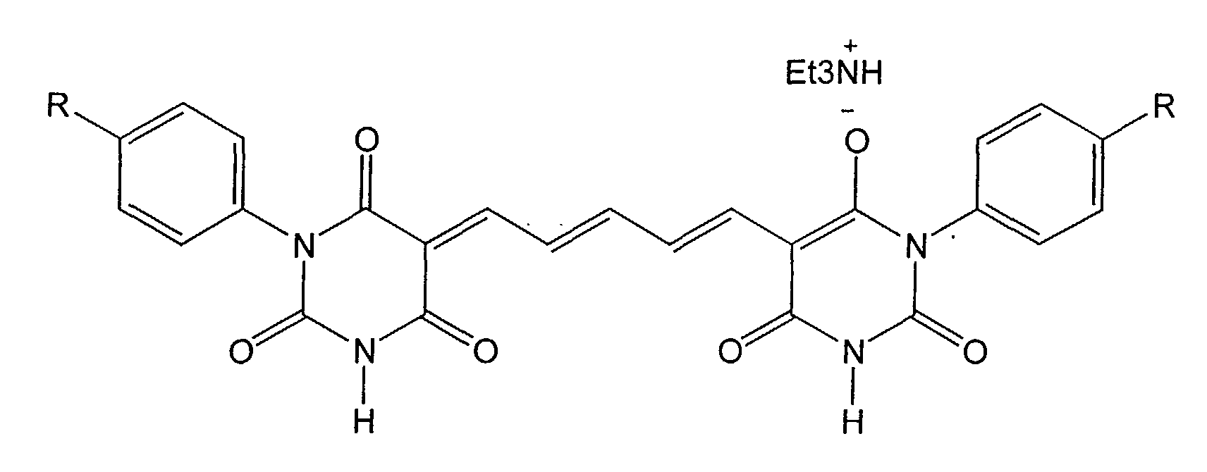
at 220 mg/sq.m. - The protective gelatin overcoat contained surfactants and was coated at a gelatin laydown of 1.465 g/sq.m. The layer also contained hydroquinone at 162.2 mg/sq.m and a solid particle safelight protection dye of structureat 140 mg/sq.m.

- The latent image forming emulsion layer consisted of a 70:30 chlorobromide cubic monodispersed emulsion (0.215 µm mean edge length) doped with a rhodium salt, chemically sensitized with sulphur and gold and spectrally sensitized with 190 mg/Ag mole of a trinuclear merocyanine sensitizing dye of structureR1 = CH2CO2H

- The emulsion was coated at silver coverages as described in Table 1 below in a matrix of 1.85 g/sq.m gelatin and a blend of latex copolymer of methyl acrylate, the sodium salt of 2-acrylamido-2-methylpropane sulphonic acid and 2-(methacryloyloxy)-ethylacetoacetate (88:5:7 by weight), (POL "A"), as shown in Table 1 below. Other addenda included 2-mercaptomethyl-5-carboxy-4-hydroxy-6-methyl-1,3,3a,7-tetraazaindene, 1-(3-acetamidophenyl)-5-mercaptotetrazole and 2,3-dihydro-2-thioxo-4-thiazoleacetic acid. The layer also contained 6.32 mg/sq.m of a nucleator compound of structure
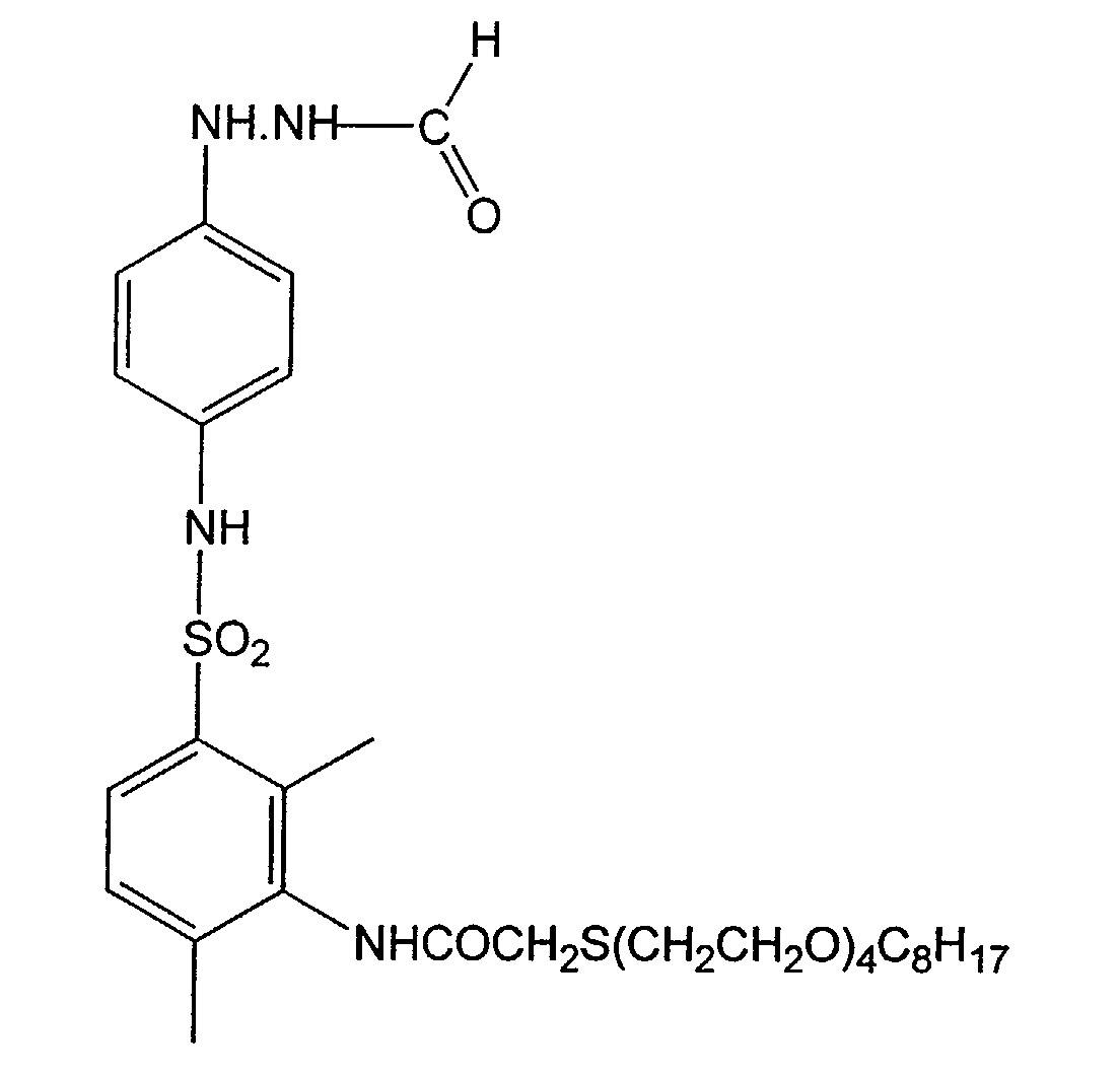
Coating Ag (g/sq.m) POL "A"
(g/sq.m)Ag/Total E-pol Ag/Total
E-MatrixAg/Total
film matrixA1 3.6 0.550 6.55 1.50 0.61 A2 3.6 1.650 2.18 1.03 0.52 A3 3.0 1.650 1.82 0.86 0.43 - Table 1 above also shows the ratio values for silver:total emulsion layer polymer, silver:total emulsion layer matrix, and silver:total film matrix.
- A line tint pattern was formed on the films as follows. The samples were exposed to WRATTEN™ 29 filtered light on a sensitometer which had been modified such that a line tint original (40µmlines and 40µmspaces) was placed over the conventional step tablet. The experimental film samples were placed in intimate contact with the tint original before the exposure was made, followed by development in KODAK ™ ACCUMAX ™ 2000RA developer (diluted 1+2) at 35 deg C for 45 seconds, followed by conventional fixing, washing and drying.
- The resultant line tint patterns were evaluated on an X-RITE ™ densitometer in "dot%" mode, such that a patch on each experimental film was found and accurately measured corresponding to a reading of approximately 35%. The area was carefully marked, and the films placed on the glass of a KODAK ™ CONTACT 2000 ™ "2800" contact frame. The films were then covered with a sheet of 25µmthick polyethylene terephthalate film support to exaggerate the effect of contact gain, and then with a sheet of KODAK ™ CONTACT 2000 ™ CA4 general purpose contact film. UV exposures were made corresponding to either 308 units exposure, or 715 units exposure. The CA4 film was processed in KODAK ™ RA2000 developer (diluted 1+4) at 35 deg C for 30 seconds, followed by conventional fixing, washing and drying.
- The "marked" areas from the originals were measured on the contact film, again using the X-RITE™ densitometer in "dot%" mode. From these measurements the difference (dot gain) from the theoretical value (approximately 65%) could be measured. In addition, the actual line width gain was calculated from the dot gain figures, Table 2.
Coating 308 units exp
dot gain (%)308 units exp
line gain (µm)715 units exp
dot gain (%)715 units exp
line gain (µm)A1 11.4 9.1 16.9 13.5 A2 9.2 7.4 14.0 11.2 A3 8.4 6.7 13.3 10.6 - It will be seen from the data in Table 2 that effect of line width gain on contacting, exaggerated using the spacer sheet between the film (photomask) and the photosensitive receiver, can be minimised by coating the minimum amount of silver, and the maximum amount of polymer, in the emulsion layer of the original photomask film material. In addition, and by reference to Table 1, it will be seen that the minimum line width gain can be obtained when the silver:emulsion layer polymer ratio is <2.0.
- Coatings B1, B2 and B3 were prepared in exactly the same way as coatings A1, A2 and A3, respectively, except that an emulsion with grains 0.185 µmin mean edge length was used, and that spectral sensitization was carried out with 240 mg/Ag mole of trinuclear merocyanine sensitizing dye.
- The samples for contacting were prepared in the same way as in Example 1, as were the subsequent evaluations. Table 3 shows the dot gain and line width gain results.
Coating 308 units exp
dot gain (%)308 units exp
line gain (µm)715 units exp
dot gain (%)715 units exp
line gain (µm)B1 10.8 8.6 16.7 13.4 B2 10.0 8.0 15.1 12.1 B3 8.0 6.4 12.6 10.1 - Again, it will be seen from the data in Table 3 that the effect of line width gain on contacting, exaggerated using a spacer sheet between the film (photomask) and the photosensitive receiver, can be minimised by coating the minimum amount of silver, and the maximum amount of polymer, in the emulsion layer of the original photomask film material. In addition, and by reference to Table 1, it will be seen that the minimum line width gain can be obtained when the silver:emulsion layer polymer ratio is <2.0.
Claims (5)
- A black and white silver halide material for optical contact copying, comprising:at least one photographic emulsion layer including a silver-halide-containing matrix in which the matrix includes a polymer and a hydrophilic binder, wherein the ratio of the weight of silver in the emulsion layer to the weight of polymer in the emulsion layer per unit area is less than 2.0.
- A material according to claim 1, in which the hydrophilic binder is gelatin.
- A material according to claim 1 or 2, in which the polymer is a polymer derived from the polymerization of one or more ethylenically unsaturated monomers.
- A material according to claim 3, in which the polymer is selected from a group consisting of acrylates, methacrylates, acrylamides and methacrylamides.
- A method of optical contact copying comprising the step of irradiating a substrate onto which a pattern is to be copied with radiation through an optical mask of the pattern, such that regions of the substrate are selectively exposed or hidden from the radiation, wherein the mask is formed of a black and white photographic material according to claim 1.
Applications Claiming Priority (2)
| Application Number | Priority Date | Filing Date | Title |
|---|---|---|---|
| GB0116682 | 2001-07-07 | ||
| GBGB0116682.6A GB0116682D0 (en) | 2001-07-07 | 2001-07-07 | Black and white photographic material |
Publications (2)
| Publication Number | Publication Date |
|---|---|
| EP1273966A1 true EP1273966A1 (en) | 2003-01-08 |
| EP1273966B1 EP1273966B1 (en) | 2008-03-12 |
Family
ID=9918134
Family Applications (1)
| Application Number | Title | Priority Date | Filing Date |
|---|---|---|---|
| EP02012607A Expired - Lifetime EP1273966B1 (en) | 2001-07-07 | 2002-06-06 | Black and white photographic material |
Country Status (5)
| Country | Link |
|---|---|
| US (1) | US6770412B2 (en) |
| EP (1) | EP1273966B1 (en) |
| JP (1) | JP2003043622A (en) |
| DE (1) | DE60225506T2 (en) |
| GB (1) | GB0116682D0 (en) |
Cited By (1)
| Publication number | Priority date | Publication date | Assignee | Title |
|---|---|---|---|---|
| WO2005054946A1 (en) * | 2003-12-04 | 2005-06-16 | Eastman Kodak Company | Photographic materials having improved keeping properties |
Families Citing this family (1)
| Publication number | Priority date | Publication date | Assignee | Title |
|---|---|---|---|---|
| WO2006033402A1 (en) * | 2004-09-24 | 2006-03-30 | Nihon University | Method for manufacturing ceramic electronic component |
Citations (5)
| Publication number | Priority date | Publication date | Assignee | Title |
|---|---|---|---|---|
| US3734616A (en) * | 1970-05-20 | 1973-05-22 | Marconi Co Ltd | Apparatus for the manufacture of printed circuits |
| EP0643326A1 (en) * | 1993-09-09 | 1995-03-15 | Agfa-Gevaert N.V. | New type of polymer latex and its use as plasticizer in a photographic material |
| EP0716338A2 (en) * | 1994-12-09 | 1996-06-12 | Fuji Photo Film Co., Ltd. | Fine polymer particles having heterogeneous phase structure, silver halide photographic light- sensitive material containing the fine polymer particles and image-forming method |
| US5691107A (en) * | 1994-12-07 | 1997-11-25 | Mitsubishi Paper Mills Limited | Silver halide photographic photosensitive material |
| EP0928987A2 (en) * | 1997-12-09 | 1999-07-14 | Eastman Kodak Company | Photographic silver halide material |
Family Cites Families (4)
| Publication number | Priority date | Publication date | Assignee | Title |
|---|---|---|---|---|
| US3647459A (en) * | 1967-06-28 | 1972-03-07 | Eastman Kodak Co | Novel photographic elements and means for rapid processing of photographic elements |
| JP2530828B2 (en) | 1987-01-09 | 1996-09-04 | コニカ株式会社 | Silver halide photographic light-sensitive material for semiconductor laser light source |
| DE69123113T2 (en) * | 1990-09-14 | 1997-04-10 | Konishiroku Photo Ind | Syllable halide photographic light-sensitive material |
| EP0735416A1 (en) | 1995-03-31 | 1996-10-02 | Eastman Kodak Company | Photographic elements with particular sensitized silver halide emulsions |
-
2001
- 2001-07-07 GB GBGB0116682.6A patent/GB0116682D0/en not_active Ceased
-
2002
- 2002-06-06 DE DE60225506T patent/DE60225506T2/en not_active Expired - Lifetime
- 2002-06-06 EP EP02012607A patent/EP1273966B1/en not_active Expired - Lifetime
- 2002-06-24 US US10/178,265 patent/US6770412B2/en not_active Expired - Lifetime
- 2002-07-01 JP JP2002191703A patent/JP2003043622A/en active Pending
Patent Citations (5)
| Publication number | Priority date | Publication date | Assignee | Title |
|---|---|---|---|---|
| US3734616A (en) * | 1970-05-20 | 1973-05-22 | Marconi Co Ltd | Apparatus for the manufacture of printed circuits |
| EP0643326A1 (en) * | 1993-09-09 | 1995-03-15 | Agfa-Gevaert N.V. | New type of polymer latex and its use as plasticizer in a photographic material |
| US5691107A (en) * | 1994-12-07 | 1997-11-25 | Mitsubishi Paper Mills Limited | Silver halide photographic photosensitive material |
| EP0716338A2 (en) * | 1994-12-09 | 1996-06-12 | Fuji Photo Film Co., Ltd. | Fine polymer particles having heterogeneous phase structure, silver halide photographic light- sensitive material containing the fine polymer particles and image-forming method |
| EP0928987A2 (en) * | 1997-12-09 | 1999-07-14 | Eastman Kodak Company | Photographic silver halide material |
Cited By (1)
| Publication number | Priority date | Publication date | Assignee | Title |
|---|---|---|---|---|
| WO2005054946A1 (en) * | 2003-12-04 | 2005-06-16 | Eastman Kodak Company | Photographic materials having improved keeping properties |
Also Published As
| Publication number | Publication date |
|---|---|
| JP2003043622A (en) | 2003-02-13 |
| US6770412B2 (en) | 2004-08-03 |
| EP1273966B1 (en) | 2008-03-12 |
| GB0116682D0 (en) | 2001-08-29 |
| DE60225506D1 (en) | 2008-04-24 |
| DE60225506T2 (en) | 2009-04-23 |
| US20030036026A1 (en) | 2003-02-20 |
Similar Documents
| Publication | Publication Date | Title |
|---|---|---|
| US4183990A (en) | Step tablet | |
| GB1577492A (en) | Photohardenable elements | |
| JPS59121327A (en) | Photographic sensitive silver halide material for photomechanical process and method for reducing it | |
| US3985561A (en) | Diffusion transfer process using silver halide emulsions with 90% chloride and high binder to silver halide ratios | |
| US6770412B2 (en) | Black and white photographic material | |
| US3249436A (en) | Process for preparing printing plates from photopolymerizable materials by the use of a masking technique | |
| CA1055759A (en) | Production of planographic printing patterns | |
| US3747525A (en) | Treating a developed gelatin silver halide emulsion layer element with acetic acid and dischromate ions | |
| JPH02306237A (en) | Image forming method | |
| EP0298158A1 (en) | Silver complex diffusion transfer processing | |
| JPH08194315A (en) | Diffusion-transfer printing plate | |
| US3976487A (en) | Photosensitive printing plate | |
| US5330875A (en) | Process for producing negative and positive original images on a bilevel printing plate utilizing non-silver halide layer and silver halide overlayer | |
| GB1569109A (en) | Lippmann-emulsions and reversal processing thereof | |
| EP1482362B1 (en) | Planographic printing plate material, printing plate and printing method | |
| JPS59101646A (en) | Photosensitive silver halide material for daylight room | |
| US4357407A (en) | Production of reverse reading positive images of a straight reading original | |
| US5348846A (en) | Silver halide photographic photosensitive material | |
| EP0558555B1 (en) | Diffusion transfer receiver | |
| JPH03238446A (en) | Silver halide photographic sensitive material | |
| JP3305488B2 (en) | Lithographic printing plate | |
| JPS6075838A (en) | Lithographic printing plate | |
| Mizuki | Sensitive Materials For Image Instrumentation | |
| JP3473816B2 (en) | Silver halide photographic materials | |
| JP2651241B2 (en) | Manufacturing method of lithographic printing plate for scanning exposure |
Legal Events
| Date | Code | Title | Description |
|---|---|---|---|
| PUAI | Public reference made under article 153(3) epc to a published international application that has entered the european phase |
Free format text: ORIGINAL CODE: 0009012 |
|
| AK | Designated contracting states |
Kind code of ref document: A1 Designated state(s): AT BE CH CY DE DK ES FI FR GB GR IE IT LI LU MC NL PT SE TR |
|
| AX | Request for extension of the european patent |
Free format text: AL;LT;LV;MK;RO;SI |
|
| 17P | Request for examination filed |
Effective date: 20030528 |
|
| AKX | Designation fees paid |
Designated state(s): DE FR GB |
|
| 17Q | First examination report despatched |
Effective date: 20050407 |
|
| GRAP | Despatch of communication of intention to grant a patent |
Free format text: ORIGINAL CODE: EPIDOSNIGR1 |
|
| GRAS | Grant fee paid |
Free format text: ORIGINAL CODE: EPIDOSNIGR3 |
|
| GRAA | (expected) grant |
Free format text: ORIGINAL CODE: 0009210 |
|
| AK | Designated contracting states |
Kind code of ref document: B1 Designated state(s): DE |
|
| RBV | Designated contracting states (corrected) |
Designated state(s): DE |
|
| REF | Corresponds to: |
Ref document number: 60225506 Country of ref document: DE Date of ref document: 20080424 Kind code of ref document: P |
|
| PLBE | No opposition filed within time limit |
Free format text: ORIGINAL CODE: 0009261 |
|
| STAA | Information on the status of an ep patent application or granted ep patent |
Free format text: STATUS: NO OPPOSITION FILED WITHIN TIME LIMIT |
|
| 26N | No opposition filed |
Effective date: 20081215 |
|
| PGFP | Annual fee paid to national office [announced via postgrant information from national office to epo] |
Ref country code: DE Payment date: 20190515 Year of fee payment: 18 |
|
| REG | Reference to a national code |
Ref country code: DE Ref legal event code: R119 Ref document number: 60225506 Country of ref document: DE |
|
| PG25 | Lapsed in a contracting state [announced via postgrant information from national office to epo] |
Ref country code: DE Free format text: LAPSE BECAUSE OF NON-PAYMENT OF DUE FEES Effective date: 20210101 |