EP1271634A2 - Methods for forming low-K dielectric films - Google Patents
Methods for forming low-K dielectric films Download PDFInfo
- Publication number
- EP1271634A2 EP1271634A2 EP02254247A EP02254247A EP1271634A2 EP 1271634 A2 EP1271634 A2 EP 1271634A2 EP 02254247 A EP02254247 A EP 02254247A EP 02254247 A EP02254247 A EP 02254247A EP 1271634 A2 EP1271634 A2 EP 1271634A2
- Authority
- EP
- European Patent Office
- Prior art keywords
- linking agent
- low
- polyhedral oligomeric
- oligomeric silsesquioxane
- peroxide
- Prior art date
- Legal status (The legal status is an assumption and is not a legal conclusion. Google has not performed a legal analysis and makes no representation as to the accuracy of the status listed.)
- Withdrawn
Links
Classifications
-
- H—ELECTRICITY
- H10—SEMICONDUCTOR DEVICES; ELECTRIC SOLID-STATE DEVICES NOT OTHERWISE PROVIDED FOR
- H10P—GENERIC PROCESSES OR APPARATUS FOR THE MANUFACTURE OR TREATMENT OF DEVICES COVERED BY CLASS H10
- H10P14/00—Formation of materials, e.g. in the shape of layers or pillars
- H10P14/60—Formation of materials, e.g. in the shape of layers or pillars of insulating materials
- H10P14/69—Inorganic materials
- H10P14/692—Inorganic materials composed of oxides, glassy oxides or oxide-based glasses
- H10P14/6921—Inorganic materials composed of oxides, glassy oxides or oxide-based glasses containing silicon
- H10P14/6922—Inorganic materials composed of oxides, glassy oxides or oxide-based glasses containing silicon the material containing Si, O and at least one of H, N, C, F or other non-metal elements, e.g. SiOC, SiOC:H or SiONC
-
- C—CHEMISTRY; METALLURGY
- C23—COATING METALLIC MATERIAL; COATING MATERIAL WITH METALLIC MATERIAL; CHEMICAL SURFACE TREATMENT; DIFFUSION TREATMENT OF METALLIC MATERIAL; COATING BY VACUUM EVAPORATION, BY SPUTTERING, BY ION IMPLANTATION OR BY CHEMICAL VAPOUR DEPOSITION, IN GENERAL; INHIBITING CORROSION OF METALLIC MATERIAL OR INCRUSTATION IN GENERAL
- C23C—COATING METALLIC MATERIAL; COATING MATERIAL WITH METALLIC MATERIAL; SURFACE TREATMENT OF METALLIC MATERIAL BY DIFFUSION INTO THE SURFACE, BY CHEMICAL CONVERSION OR SUBSTITUTION; COATING BY VACUUM EVAPORATION, BY SPUTTERING, BY ION IMPLANTATION OR BY CHEMICAL VAPOUR DEPOSITION, IN GENERAL
- C23C16/00—Chemical coating by decomposition of gaseous compounds, without leaving reaction products of surface material in the coating, i.e. chemical vapour deposition [CVD] processes
- C23C16/22—Chemical coating by decomposition of gaseous compounds, without leaving reaction products of surface material in the coating, i.e. chemical vapour deposition [CVD] processes characterised by the deposition of inorganic material, other than metallic material
- C23C16/30—Deposition of compounds, mixtures or solid solutions, e.g. borides, carbides, nitrides
- C23C16/40—Oxides
- C23C16/401—Oxides containing silicon
-
- H—ELECTRICITY
- H10—SEMICONDUCTOR DEVICES; ELECTRIC SOLID-STATE DEVICES NOT OTHERWISE PROVIDED FOR
- H10P—GENERIC PROCESSES OR APPARATUS FOR THE MANUFACTURE OR TREATMENT OF DEVICES COVERED BY CLASS H10
- H10P14/00—Formation of materials, e.g. in the shape of layers or pillars
- H10P14/60—Formation of materials, e.g. in the shape of layers or pillars of insulating materials
- H10P14/63—Formation of materials, e.g. in the shape of layers or pillars of insulating materials characterised by the formation processes
- H10P14/6326—Deposition processes
- H10P14/6328—Deposition from the gas or vapour phase
- H10P14/6334—Deposition from the gas or vapour phase using decomposition or reaction of gaseous or vapour phase compounds, i.e. chemical vapour deposition
-
- H—ELECTRICITY
- H10—SEMICONDUCTOR DEVICES; ELECTRIC SOLID-STATE DEVICES NOT OTHERWISE PROVIDED FOR
- H10P—GENERIC PROCESSES OR APPARATUS FOR THE MANUFACTURE OR TREATMENT OF DEVICES COVERED BY CLASS H10
- H10P14/00—Formation of materials, e.g. in the shape of layers or pillars
- H10P14/60—Formation of materials, e.g. in the shape of layers or pillars of insulating materials
- H10P14/66—Formation of materials, e.g. in the shape of layers or pillars of insulating materials characterised by the type of materials
- H10P14/668—Formation of materials, e.g. in the shape of layers or pillars of insulating materials characterised by the type of materials the materials being characterised by the deposition precursor materials
- H10P14/6681—Formation of materials, e.g. in the shape of layers or pillars of insulating materials characterised by the type of materials the materials being characterised by the deposition precursor materials the precursor containing a compound comprising Si
- H10P14/6682—Formation of materials, e.g. in the shape of layers or pillars of insulating materials characterised by the type of materials the materials being characterised by the deposition precursor materials the precursor containing a compound comprising Si the compound being a silane, e.g. disilane, methylsilane or chlorosilane
-
- H—ELECTRICITY
- H10—SEMICONDUCTOR DEVICES; ELECTRIC SOLID-STATE DEVICES NOT OTHERWISE PROVIDED FOR
- H10P—GENERIC PROCESSES OR APPARATUS FOR THE MANUFACTURE OR TREATMENT OF DEVICES COVERED BY CLASS H10
- H10P14/00—Formation of materials, e.g. in the shape of layers or pillars
- H10P14/60—Formation of materials, e.g. in the shape of layers or pillars of insulating materials
- H10P14/63—Formation of materials, e.g. in the shape of layers or pillars of insulating materials characterised by the formation processes
- H10P14/6326—Deposition processes
- H10P14/6328—Deposition from the gas or vapour phase
- H10P14/6334—Deposition from the gas or vapour phase using decomposition or reaction of gaseous or vapour phase compounds, i.e. chemical vapour deposition
- H10P14/6336—Deposition from the gas or vapour phase using decomposition or reaction of gaseous or vapour phase compounds, i.e. chemical vapour deposition in the presence of a plasma [PECVD]
-
- H—ELECTRICITY
- H10—SEMICONDUCTOR DEVICES; ELECTRIC SOLID-STATE DEVICES NOT OTHERWISE PROVIDED FOR
- H10P—GENERIC PROCESSES OR APPARATUS FOR THE MANUFACTURE OR TREATMENT OF DEVICES COVERED BY CLASS H10
- H10P14/00—Formation of materials, e.g. in the shape of layers or pillars
- H10P14/60—Formation of materials, e.g. in the shape of layers or pillars of insulating materials
- H10P14/66—Formation of materials, e.g. in the shape of layers or pillars of insulating materials characterised by the type of materials
- H10P14/665—Porous materials
-
- H—ELECTRICITY
- H10—SEMICONDUCTOR DEVICES; ELECTRIC SOLID-STATE DEVICES NOT OTHERWISE PROVIDED FOR
- H10P—GENERIC PROCESSES OR APPARATUS FOR THE MANUFACTURE OR TREATMENT OF DEVICES COVERED BY CLASS H10
- H10P14/00—Formation of materials, e.g. in the shape of layers or pillars
- H10P14/60—Formation of materials, e.g. in the shape of layers or pillars of insulating materials
- H10P14/66—Formation of materials, e.g. in the shape of layers or pillars of insulating materials characterised by the type of materials
- H10P14/668—Formation of materials, e.g. in the shape of layers or pillars of insulating materials characterised by the type of materials the materials being characterised by the deposition precursor materials
- H10P14/6681—Formation of materials, e.g. in the shape of layers or pillars of insulating materials characterised by the type of materials the materials being characterised by the deposition precursor materials the precursor containing a compound comprising Si
- H10P14/6684—Formation of materials, e.g. in the shape of layers or pillars of insulating materials characterised by the type of materials the materials being characterised by the deposition precursor materials the precursor containing a compound comprising Si the compound comprising silicon and oxygen
- H10P14/6686—Formation of materials, e.g. in the shape of layers or pillars of insulating materials characterised by the type of materials the materials being characterised by the deposition precursor materials the precursor containing a compound comprising Si the compound comprising silicon and oxygen the compound being a molecule comprising at least one silicon-oxygen bond and the compound having hydrogen or an organic group attached to the silicon or oxygen, e.g. a siloxane
Definitions
- the present invention provides for methods for forming a low-k dielectric film on semiconductor or integrated circuits employing a polyhedral oligomeric silsesquioxane. More particularly, the present invention provides for using the polyhedral oligomeric silsesquioxane and a polymer linking agent to form a structure that when applied as a film will have an ultra low-k dielectric constant less than or equal to 2.6.
- the increase in semiconductor design integration by feature size reduction has resulted in increased levels of interconnect and increased utilization of dielectric low-k thin films.
- the dielectric film is used as insulation around metal lines of a device and contributes to the RC time constant that controls the device speed.
- R resistance
- C capacitance
- Reducing capacitance by lowering the dielectric constant k to the inter and intra level dielectric (ILD) film can improve device performance by reducing the RC time delay, decreasing the cross talk between adjacent metal lines and lowering the power dissipation.
- the material of choice for the ILD is silicon dioxide (SiO 2 ) which can be prepared using silane, disilane or siloxane precursors in an oxidizing environment.
- the most popular deposition techniques for depositing ILD are chemical vapor deposition (CVD), low temperature plasma-enhanced CVD (PECVD), or high density plasma CVD (HDPCVD).
- CVD chemical vapor deposition
- PECVD low temperature plasma-enhanced CVD
- HDPCVD high density plasma CVD
- the dielectric constant of the deposited SiO 2 is relatively high at 4.0.
- low-k materials must have smaller dielectric constants. Industry publications have indicated that low-k materials with k values from 2.7 to 3.5 would be needed for 150 and 130 nm technology modes. When the industry moves to 100 nm technology and dimensions below that in the future, extra low-k (ELK) materials having a k value from 2.2 to 2.6 and ultra low-k (ULK) materials with a k value less than 2.2 will be necessary.
- ELK extra low-k
- ULK ultra low-k
- the semiconductor industry has developed several low-k materials to replace silicon dioxide that are inorganic, organic or hybrid materials. These materials can be deposited by either chemical vapor deposition (CVD) or spin-on deposition (SOD) methods.
- CVD chemical vapor deposition
- SOD spin-on deposition
- the CVD technique utilizes existing vacuum tools for depositing SiO 2 that include lower temperature plasma enhanced CVD (PECVD) and high density plasma CVD (HDP-CVD).
- PECVD lower temperature plasma enhanced CVD
- HDP-CVD high density plasma CVD
- the SOD method uses spin coaters that have shown better extendibility to ELK or ULK by introducing pores in nanometer sizes.
- Newer materials such as fluorosilicate glass (FSG), carbon or carbon fluorine based films and carbon-doped SiO 2 utilize CVD techniques.
- Materials such as polyimide, hydrogen silsesquioxane (HSQ) and polyarylene ethers can be deposited using SOD techniques.
- the present invention provides for new materials for use as extra low dielectric CVD precursors in extra low-k CVD materials for the semiconductor industry.
- the present invention provides a novel class of compounds useful for forming a film on a semiconductor or integrated circuit by acting as a precursor for the film formed when the compound is applied.
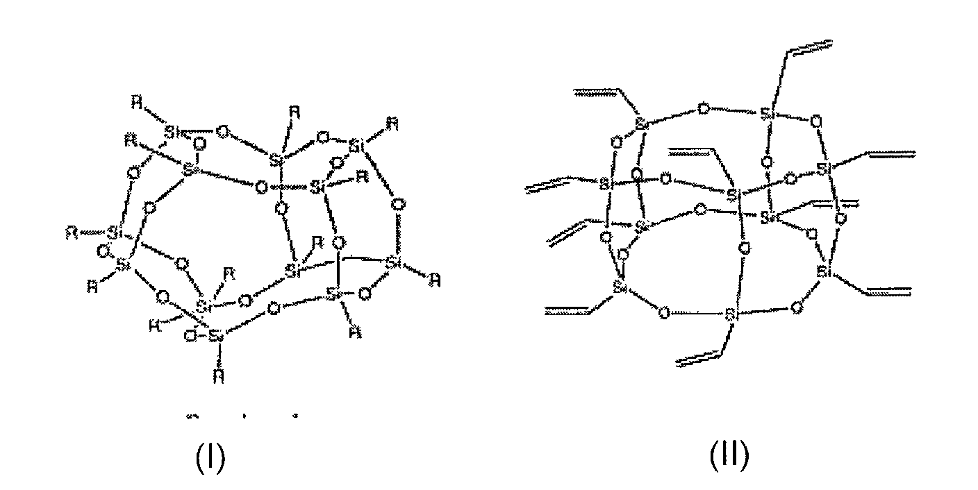
- Polyhedral oligomeric silsesquioxane having a variety of functional groups attached to a silicon oxide cage structure of the molecule, are employed in either a thermal chemical vapor deposition chamber or a plasma enhanced chemical vapor deposition chamber to form an ultra low-k dielectric film on the surface of semiconductors and integrated circuits.
- the POSS molecule when combined with a linking agent in the CVD chambers, will react and polymerize to form the low-k dielectric film.
- the present invention relates to a method of forming a low-k dielectric film on the surface of a semiconductor or an integrated circuit comprising reacting in a chemical vapor deposition chamber a polyhedral oligomeric silsesquioxane (POSS) with a polymeric linking agent thereby depositing on the semiconductor or integrated circuit surface and forming an extra or ultra low-k dielectric where K is less than or equal to 2.6.
- PES polyhedral oligomeric silsesquioxane
- R 1 , R 2 , and R 3 are preferably selected from the group consisting of vinyl, oxymethyl, oxyethyl, phenyl, cyclopentyl, cyclohexyl, isobutyl, norborenal, norborenoethyl, norbornenyl, chlorosilane, silanol, alcohol, acrylates, particularly methacrylate, esters and epoxides.
- siloxanes having the general formula (-OSiH X (CH 3 ) 3-X ) where x is 1 to 3.
- the linking agents are employed to react with the POSS molecule thereby polymerizing forming a polymerized molecular POSS structure into a continuous film formed on the semiconductor or integrated circuit surface. This reaction will occur via radical polymerization.
- the linking agents may be selected from the group comprising, but not limited to, methylsilane, dimethylsilane, silane, disilane, vinylmethyldimethylcyclotrisiloxane, dimethylsila-oxocyclopentane, cyclohexylsilane, cyclohexyldisilane, silacyclobutane, tetramethyldisiloxane, cyclooctylsilane, vinylmethylsilane, cyclopentylsilane, (mono- or di-)tert-butyl silane, tert-butylphenylsilane, methyldisilane, tetraethyl-ethylsilicate, tetramethyle
- the R and R' groups in the disiloxane may be selected from the group consisting of hydrogen, methyl, ethyl, tert-butyl, vinyl, ethoxy, methoxy, phenyl and halogens.
- Other linking agents may also include straight chain siloxanes such as Si n O (n-1) (CH3) 2n H 2 where n is 3 to 8.
- organic peroxides such as benzoyl peroxide, acetyl-benzoyl peroxide, diacetyl peroxide, ditert-butyl peroxide, dimethyl peroxide and other alkyl peroxides having C 1 to C 5 (i.e. from 1 to 5 carbon atoms) are effective as linking agents in the present invention.
- the compounds containing the silyl groups are particularly suitable for formation of radicals to link one POSS functional group to another POSS functional group by stabilizing radical formation.
- Cyclotrisiloxane and cyclooctasilane contain large ring structures which can further increase the space between the POSS group as they link to one another during the polymerization.
- These large linking agents in the radical polymerization CVD can further reduce the dielectric constant using the POSS molecules and the linking agents.
- Silicon compounds with tert-butyl groups will also help stabilize the silyl radicals and the t-butyl groups may act as "leaving groups" that will increase porosity of the film during subsequent anneals at 250-400 C in a hydrogen environment.
- Partial oxidation to remove hydrogen atoms can be employed by forming silyl radicals by the following example. 2 R-SiH 3 + O 2 ⁇ 2 R-SiH 2 + 2 H 2 O
- silane When there is a deficit of oxygen, silane has been known to form silyl radicals which stay in a metastable state (which can be stabilized by appropriate choice of functional groups such as t-butyl or cyclo-organics). This metastable state is maintained until the silyl radical combines with another functional group sometimes in an explosive manner. This tendency to form silyl radicals can be exploited by putting a small quantity of oxygen, ozone or peroxide compound in contact with the silyl groups on several of the linking agents described above and forming the silyl radicals. Methyl radicals may also be formed in a similar manner, but they are even less stable. The less stable methyl radicals may also participate in this reaction.
- the silicon oxide cages of the POSS molecule may also be open such that the functional materials from the polymeric linking agent attach to the open side of the silicon oxide cage.
- Plasmas are known to create radicals by electronic bombardment in a plasma field.
- Methylsilane radicals can be formed by creating plasma with or without the presence of a small quantity of oxygen that activates the methylsilane. These radicals can then subsequently react with the functional groups on the vaporized POSS material.
- the other linking agents may be treated in a manner similar to that of the methylsilane to create radicals that are then employed to polymerize with the gas phase POSS delivered into the CVD chamber.
- the POSS compound is a solid, generally a white crystalline powder.
- materials having the POSS formula are volatile under typical CVD conditions.
- the POSS material will be dissolved in an appropriate solvent of moderate volatility such as cyclohexane, benzene, normal and cyclo-siloxanes, volatile silicone solvents, tetrahydrofuran and certain of the linking agents suggested earlier, particularly the volatile silanes, siloxanes and organosiloxanes.
- an appropriate solvent of moderate volatility such as cyclohexane, benzene, normal and cyclo-siloxanes, volatile silicone solvents, tetrahydrofuran and certain of the linking agents suggested earlier, particularly the volatile silanes, siloxanes and organosiloxanes.
- the solvent interferes with the plasma formation, the POSS material can be delivered as a sublimed solid in a pure form to the CVD chamber.
- the solution is injected into a region of the reactor where the pressure is between 0.1 and 10 torr and the solution is heated above the vaporization point as measured at 1 torr for the selected POSS material. Typically, this is around 100
- the radicals are generated by partial reaction with oxygen in the thermal reactor chamber or by passing through a plasma region which will create linking agent radicals that will also combine with the POSS and solvent materials. This combined flow will then pass over the heated wafer which is heated from 200 to 450°C depending upon the appropriate combined POSS material and linking agent's properties.
- the semiconductor substrate or integrated circuit is typically a silicon wafer and can be up to 300 mm in diameter.
- POSS film Some advantages of using POSS film include: (1) internal free space can be selected at the precursor level. Comparison can be made to the density with SiO 2 film to see the reduction; (2) free space between POSS cages can be engineered using different types of linkage precursor; and (3) thermal-mechanical strength, hardness, modulus, thermal stability, surface roughness, etc. can be engineered by selection of the appropriate linkage precursor and deposition conditions.
- the solution was sprayed into the chamber using an ultrasonic nebulizer designed to deliver the solution in 20 ⁇ L droplets allowing for the complete vaporization before coming in contact with a 100 mm (4 inch) wafer, which is heated to 250°C.
- methylsilane (MMS) was flowing at 100 sccm and oxygen was flowing at 20 sccm entering into the chamber via a manifold directly above the MMS manifold. Reaction occurred on the wafer creating a 30 micron localized deposition. In comparing this to deposition on a wafer which is generated by the reaction of methylsilane, oxygen and cyclohexane in the absence of a POSS material, one fifth of the thickness of deposition occurred. This demonstrates the polymerization reaction takes place on the wafer due to the interaction of the methylsilane linking agent and the POSS material.
- POSS may be delivered without a solvent by using a PECVD chamber with a sublimation chamber. Either AC or DC plasma is struck between the methylsilane, oxygen showerhead and the hotplate.
- the vinyl POSS material is heated in an outboard chamber that is about 0.1 to 5 torr chamber pressure.
- the POSS chamber is heated above the 200-300°C temperatures necessary to volatize the POSS at the pressures of the chamber.
- the POSS vapor is carried to the chamber using an inert gas flow, typically argon, the hotplate holding the wafer is heated to 200-300°C.
- the monomethylsilane radicals from the plasma react with the POSS functional groups and form the low-k dielectric material on the wafer.
- POSS C 16 H 56 O 20 Si 16
- 8 siloxane groups with 2 methyl and one hydrogen group on each silicon in each functional group is dissolved (4% by weight) in cyclohexane.
- Four ml/min of liquid is injected into the thermal CVD chamber.
- the solution is heated in the chamber to 250 C in a heated metal mesh at 1-5 torr chamber pressure.
- the vaporized gases then passes through two ring manifolds.
- the first manifold supplies 100 sccm of hexamethyl dihydro trisiloxane (vapor from a vessel of the liquid heated to 128C) and the second supplies 40 sccm of oxygen.
- the siloxane functional groups on the POSS and trisiloxane react with O2 in a partial oxidation reaction that reacts with some of the hydrogen atoms on the compounds, forming radicals. These radicals polymerize on the 250 C substrate wafer to form a low-k deposit.
- the monomethylsilane and trisiloxane compounds bridge between the siloxane functional groups on the POSS forming additional cage structure.
Landscapes
- Chemical & Material Sciences (AREA)
- Inorganic Chemistry (AREA)
- General Chemical & Material Sciences (AREA)
- Chemical Kinetics & Catalysis (AREA)
- Engineering & Computer Science (AREA)
- Materials Engineering (AREA)
- Mechanical Engineering (AREA)
- Metallurgy (AREA)
- Organic Chemistry (AREA)
- Formation Of Insulating Films (AREA)
Abstract
Description

Claims (13)
- A method of depositing a low-k dielectric film on a semiconductor or integrated circuit surface comprising reacting a polyhedral oligomeric silsesquioxane and a linking agent in a chemical vapor deposition process thereby forming said low-k dielectric film.
- A method of depositing a low-k dielectric film on a semiconductor or integrated circuit surface comprising reacting a polyhedral oligomeric silsesquioxane and a linking agent in the presence of a plasma in a chemical vapor deposition process thereby forming said low-k dielectric film.
- A method as claimed in claim 1 or claim 2, wherein said polyhedral oligomeric silsesquioxane compound has the formula SinO1.5n (R1)i(R2)j(R3)k, wherein n=i+j+k and is from 6 to 20, wherein R1, R2, and R3 are organic or silicon functional groups or a combination of both groups.
- A method as claimed in claim 3, wherein n is 8, 10 or 12.
- A method as claimed in claim 3 or claim 4, wherein said R1, R2, and R3 are selected from the group consisting of vinyl, oxymethyl, oxyethyl, pentyl, cyclopentyl, cyclohexyl, isobutyl, norborenal, norborenoethyl, norbornenyl, chlorosilane, silanol, alcohol, methacrylate, esters, hydromethylsiloxyl and epoxide functional groups
- A method as claimed in claim 3, wherein said linking agent is a straight chain (acyclic) or cyclic siloxane.
- A method as claimed in claim 6, wherein said straight chain (acyclic) siloxane isa) a disiloxane of the formula Rn(R1)6-nOSi2, wherein n is 1 to 6 and R and R1 are both selected from hydrogen, halogens, and methyl, ethyl, tert-butyl, vinyl, ethoxy, methoxy, and phenyl groups; orb) has the formula SinO(n-1)(CH3)2nH2, where n is 3 to 8,
or said cyclic siloxane has the formula OxSix(Hi)(CH3)j , where i+j=2x - A method as claimed in claim 1 or claim 2, wherein said linking agent is selected from the group consisting of methylsilane, dimethylsilane, silane, disilane, vinylmethyldimethylcyclotrisiloxane, dimethylsila-oxocyclopentane, cyclohexylsilane, cyclohexyldisilane, silacyclobutane, tetramethyldisiloxane, cyclooctylsilane, vinylmethylsilane, cyclopentylsilane, tert-butylphenylsilane, methyldisilane, tetraethyl-ethylsilicate, tetramethylethylsilicate, dimethyldioxymethylsilane, silylbenzene, disilylbenzene, trisilylbenzene, disilylcyclohexane and disiloxanes having the formula Rn(R')6-nOSi2 wherein R and R' are individually selected from the groups consisting of hydrogen, methyl, ethyl, tert-butyl, vinyl, ethoxy, methoxy, phenyl and halogen and n is 0 to 5.
- A method as claimed in claim 1, wherein said linking agent is an organic peroxide selected from the group consisting of benzoyl peroxide, acetyl-benzoyl peroxide, diacetyl peroxide, ditert-butyl peroxide, dimethyl peroxide and other alkyl peroxides having from one to five carbon atoms.
- A method as claimed in any one of the preceding claims, wherein said polyhedral oligomeric silsesquioxane is dissolved in a solvent prior to addition to said chemical vapor deposition system.
- A method as claimed in claim 10, wherein said solvent is selected from the group consisting of cyclohexane, benzene, normal and cyclo-siloxanes, volatile silicone solvents, straight chain and cylo-siloxanes with methyl and hydro functional groups and tetrahydofuran.
- A method as claimed in any one of claims 1 to 9, wherein said polyhedral oligomeric silsesquioxane is sublimed in a vacuum chamber by a direct sublimation heater in the chemical vapor deposition system.
- The use of a polyhedral oligomeric silsesquioxane to react with a linking agent in a chemical vapour deposition process to form a low dielectric constant (k) film on the surface of a semiconductor or integrated circuit.
Applications Claiming Priority (4)
| Application Number | Priority Date | Filing Date | Title |
|---|---|---|---|
| US121270 | 1987-11-16 | ||
| US29940901P | 2001-06-19 | 2001-06-19 | |
| US299409P | 2001-06-19 | ||
| US10/121,270 US6936537B2 (en) | 2001-06-19 | 2002-04-12 | Methods for forming low-k dielectric films |
Publications (2)
| Publication Number | Publication Date |
|---|---|
| EP1271634A2 true EP1271634A2 (en) | 2003-01-02 |
| EP1271634A3 EP1271634A3 (en) | 2006-04-19 |
Family
ID=26819296
Family Applications (1)
| Application Number | Title | Priority Date | Filing Date |
|---|---|---|---|
| EP02254247A Withdrawn EP1271634A3 (en) | 2001-06-19 | 2002-06-18 | Methods for forming low-K dielectric films |
Country Status (6)
| Country | Link |
|---|---|
| US (1) | US6936537B2 (en) |
| EP (1) | EP1271634A3 (en) |
| JP (1) | JP2003045870A (en) |
| KR (1) | KR20020096963A (en) |
| SG (1) | SG108850A1 (en) |
| TW (1) | TW548783B (en) |
Cited By (5)
| Publication number | Priority date | Publication date | Assignee | Title |
|---|---|---|---|---|
| WO2004114732A1 (en) * | 2003-06-19 | 2004-12-29 | World Properties, Inc. | Material including a liquid crystalline polymer and a polyhedral oligomeric silsesquioxane (poss) filler |
| WO2005004220A1 (en) * | 2003-07-03 | 2005-01-13 | Degussa Ag | Process for producing low-k dielectric films |
| US7223517B2 (en) | 2003-08-05 | 2007-05-29 | International Business Machines Corporation | Lithographic antireflective hardmask compositions and uses thereof |
| EP2242730A1 (en) * | 2008-02-15 | 2010-10-27 | Guardian Industries Corp. | Organosiloxane inclusive precursors having ring and/or cage-like structures for use in combustion deposition |
| EP4369062A1 (en) | 2022-11-14 | 2024-05-15 | Essilor International | Article coated with a low refractive index layer based on organic silsesquioxane compounds |
Families Citing this family (51)
| Publication number | Priority date | Publication date | Assignee | Title |
|---|---|---|---|---|
| US7820761B2 (en) | 1999-08-04 | 2010-10-26 | Hybrid Plastics, Inc. | Metallized nanostructured chemicals as cure promoters |
| US20060127583A1 (en) * | 2003-12-18 | 2006-06-15 | Lichtenhan Joseph D | Polyhedral oligomeric silsesquioxanes and polyhedral oligomeric silicates barrier materials for packaging |
| US20060263531A1 (en) * | 2003-12-18 | 2006-11-23 | Lichtenhan Joseph D | Polyhedral oligomeric silsesquioxanes as glass forming coatings |
| US6576345B1 (en) * | 2000-11-30 | 2003-06-10 | Novellus Systems Inc | Dielectric films with low dielectric constants |
| JP3505520B2 (en) * | 2001-05-11 | 2004-03-08 | 松下電器産業株式会社 | Interlayer insulating film |
| US7541200B1 (en) | 2002-01-24 | 2009-06-02 | Novellus Systems, Inc. | Treatment of low k films with a silylating agent for damage repair |
| KR101227664B1 (en) | 2002-01-31 | 2013-01-29 | 도소 가부시키가이샤 | Material for insulation film comprising organosilane compound, its manufacturing method and semiconductor device |
| US6873026B1 (en) * | 2002-03-04 | 2005-03-29 | Novellus Systems, Inc. | Inhomogeneous materials having physical properties decoupled from desired functions |
| US20040033371A1 (en) * | 2002-05-16 | 2004-02-19 | Hacker Nigel P. | Deposition of organosilsesquioxane films |
| TWI282124B (en) * | 2002-11-28 | 2007-06-01 | Tosoh Corp | Insulating film material containing an organic silane compound, its production method and semiconductor device |
| US7176144B1 (en) * | 2003-03-31 | 2007-02-13 | Novellus Systems, Inc. | Plasma detemplating and silanol capping of porous dielectric films |
| US7241704B1 (en) | 2003-03-31 | 2007-07-10 | Novellus Systems, Inc. | Methods for producing low stress porous low-k dielectric materials using precursors with organic functional groups |
| US7208389B1 (en) | 2003-03-31 | 2007-04-24 | Novellus Systems, Inc. | Method of porogen removal from porous low-k films using UV radiation |
| US7265061B1 (en) | 2003-05-09 | 2007-09-04 | Novellus Systems, Inc. | Method and apparatus for UV exposure of low dielectric constant materials for porogen removal and improved mechanical properties |
| US20040266184A1 (en) * | 2003-06-30 | 2004-12-30 | Ramachandrarao Vijayakumar S | Post-deposition modification of interlayer dielectrics |
| US6958291B2 (en) * | 2003-09-04 | 2005-10-25 | Taiwan Semiconductor Manufacturing Co., Ltd. | Interconnect with composite barrier layers and method for fabricating the same |
| DE10343411B4 (en) * | 2003-09-19 | 2009-07-23 | Gallus Druckmaschinen Gmbh | Rotary printing machine and method for making freely accessible a printing cylinder or a linear guide cylinder |
| US7390537B1 (en) | 2003-11-20 | 2008-06-24 | Novellus Systems, Inc. | Methods for producing low-k CDO films with low residual stress |
| JP4434146B2 (en) * | 2003-11-28 | 2010-03-17 | 日本電気株式会社 | Porous insulating film, method of manufacturing the same, and semiconductor device using the porous insulating film |
| RU2006125722A (en) * | 2003-12-18 | 2008-01-27 | Хайбрид Плэстикс, Инк. (Us) | POLYEDRIC OLIGOMERIC SILESESQUIOXANES AND METALLIZED POLYEDRIC OLIGOMERIC SILESESQUIOXANES AS COATINGS, COMPOSITES AND ADDITIVES |
| US20090085011A1 (en) * | 2003-12-18 | 2009-04-02 | Lichtenhan Joseph D | Neutron shielding composition |
| US20080249275A1 (en) * | 2003-12-18 | 2008-10-09 | Lichtenhan Joseph D | Radiation shielding with polyhedral oligomeric silsesquioxanes and metallized additives |
| US7572515B2 (en) * | 2004-01-20 | 2009-08-11 | World Properties, Inc. | Circuit materials, circuits, multi-layer circuits, and methods of manufacture thereof |
| US7341761B1 (en) | 2004-03-11 | 2008-03-11 | Novellus Systems, Inc. | Methods for producing low-k CDO films |
| US7381662B1 (en) | 2004-03-11 | 2008-06-03 | Novellus Systems, Inc. | Methods for improving the cracking resistance of low-k dielectric materials |
| US7094713B1 (en) | 2004-03-11 | 2006-08-22 | Novellus Systems, Inc. | Methods for improving the cracking resistance of low-k dielectric materials |
| US7781351B1 (en) | 2004-04-07 | 2010-08-24 | Novellus Systems, Inc. | Methods for producing low-k carbon doped oxide films with low residual stress |
| US7253125B1 (en) | 2004-04-16 | 2007-08-07 | Novellus Systems, Inc. | Method to improve mechanical strength of low-k dielectric film using modulated UV exposure |
| US7622400B1 (en) | 2004-05-18 | 2009-11-24 | Novellus Systems, Inc. | Method for improving mechanical properties of low dielectric constant materials |
| US7326444B1 (en) | 2004-09-14 | 2008-02-05 | Novellus Systems, Inc. | Methods for improving integration performance of low stress CDO films |
| US9659769B1 (en) | 2004-10-22 | 2017-05-23 | Novellus Systems, Inc. | Tensile dielectric films using UV curing |
| US7695765B1 (en) | 2004-11-12 | 2010-04-13 | Novellus Systems, Inc. | Methods for producing low-stress carbon-doped oxide films with improved integration properties |
| US7510982B1 (en) | 2005-01-31 | 2009-03-31 | Novellus Systems, Inc. | Creation of porosity in low-k films by photo-disassociation of imbedded nanoparticles |
| US7166531B1 (en) | 2005-01-31 | 2007-01-23 | Novellus Systems, Inc. | VLSI fabrication processes for introducing pores into dielectric materials |
| US8889233B1 (en) | 2005-04-26 | 2014-11-18 | Novellus Systems, Inc. | Method for reducing stress in porous dielectric films |
| TW200714636A (en) * | 2005-09-05 | 2007-04-16 | Fuji Photo Film Co Ltd | Composition, film and producing method therefor |
| US7892985B1 (en) | 2005-11-15 | 2011-02-22 | Novellus Systems, Inc. | Method for porogen removal and mechanical strength enhancement of low-k carbon doped silicon oxide using low thermal budget microwave curing |
| US8110493B1 (en) | 2005-12-23 | 2012-02-07 | Novellus Systems, Inc. | Pulsed PECVD method for modulating hydrogen content in hard mask |
| US7381644B1 (en) | 2005-12-23 | 2008-06-03 | Novellus Systems, Inc. | Pulsed PECVD method for modulating hydrogen content in hard mask |
| US7923376B1 (en) | 2006-03-30 | 2011-04-12 | Novellus Systems, Inc. | Method of reducing defects in PECVD TEOS films |
| US7468330B2 (en) | 2006-04-05 | 2008-12-23 | International Business Machines Corporation | Imprint process using polyhedral oligomeric silsesquioxane based imprint materials |
| JP2008214454A (en) * | 2007-03-02 | 2008-09-18 | Fujifilm Corp | Insulating film forming composition |
| JP2009070722A (en) * | 2007-09-14 | 2009-04-02 | Fujifilm Corp | Composition for forming insulating film and electronic device |
| US20110068332A1 (en) * | 2008-08-04 | 2011-03-24 | The Trustees Of Princeton University | Hybrid Dielectric Material for Thin Film Transistors |
| KR101880838B1 (en) * | 2008-08-04 | 2018-08-16 | 더 트러스티즈 오브 프린스턴 유니버시티 | Hybrid dielectric material for thin film transistors |
| US8703624B2 (en) * | 2009-03-13 | 2014-04-22 | Air Products And Chemicals, Inc. | Dielectric films comprising silicon and methods for making same |
| US8431670B2 (en) | 2009-08-31 | 2013-04-30 | International Business Machines Corporation | Photo-patternable dielectric materials and formulations and methods of use |
| JP5864095B2 (en) * | 2010-02-18 | 2016-02-17 | ルネサスエレクトロニクス株式会社 | Manufacturing method of semiconductor device |
| KR101401419B1 (en) | 2012-11-30 | 2014-05-30 | 한국과학기술연구원 | Low dielectric interlayer material and method for preparing the same |
| US10325979B1 (en) * | 2018-01-02 | 2019-06-18 | Qualcomm Incorporated | High density and reliable vertical natural capacitors |
| CN113943933B (en) * | 2020-07-16 | 2023-09-29 | 江苏菲沃泰纳米科技股份有限公司 | Composite film with multilayer structure, preparation method and product thereof |
Family Cites Families (8)
| Publication number | Priority date | Publication date | Assignee | Title |
|---|---|---|---|---|
| US5165955A (en) | 1991-05-28 | 1992-11-24 | Dow Corning Corporation | Method of depositing a coating containing silicon and oxygen |
| JP3688726B2 (en) * | 1992-07-17 | 2005-08-31 | 株式会社東芝 | Manufacturing method of semiconductor device |
| US5310583A (en) | 1992-11-02 | 1994-05-10 | Dow Corning Corporation | Vapor phase deposition of hydrogen silsesquioxane resin in the presence of nitrous oxide |
| US5376409B1 (en) | 1992-12-21 | 1997-06-03 | Univ New York State Res Found | Process and apparatus for the use of solid precursor sources in liquid form for vapor deposition of materials |
| US6440550B1 (en) * | 1999-10-18 | 2002-08-27 | Honeywell International Inc. | Deposition of fluorosilsesquioxane films |
| US6472076B1 (en) | 1999-10-18 | 2002-10-29 | Honeywell International Inc. | Deposition of organosilsesquioxane films |
| US6572974B1 (en) * | 1999-12-06 | 2003-06-03 | The Regents Of The University Of Michigan | Modification of infrared reflectivity using silicon dioxide thin films derived from silsesquioxane resins |
| US6440876B1 (en) * | 2000-10-10 | 2002-08-27 | The Boc Group, Inc. | Low-K dielectric constant CVD precursors formed of cyclic siloxanes having in-ring SI—O—C, and uses thereof |
-
2002
- 2002-04-12 US US10/121,270 patent/US6936537B2/en not_active Expired - Fee Related
- 2002-05-23 SG SG200203106A patent/SG108850A1/en unknown
- 2002-06-05 TW TW091112120A patent/TW548783B/en not_active IP Right Cessation
- 2002-06-18 KR KR1020020033907A patent/KR20020096963A/en not_active Withdrawn
- 2002-06-18 EP EP02254247A patent/EP1271634A3/en not_active Withdrawn
- 2002-06-18 JP JP2002176835A patent/JP2003045870A/en active Pending
Cited By (9)
| Publication number | Priority date | Publication date | Assignee | Title |
|---|---|---|---|---|
| WO2004114732A1 (en) * | 2003-06-19 | 2004-12-29 | World Properties, Inc. | Material including a liquid crystalline polymer and a polyhedral oligomeric silsesquioxane (poss) filler |
| US7180172B2 (en) | 2003-06-19 | 2007-02-20 | World Properties, Inc. | Circuits, multi-layer circuits, and methods of manufacture thereof |
| WO2005004220A1 (en) * | 2003-07-03 | 2005-01-13 | Degussa Ag | Process for producing low-k dielectric films |
| US7410914B2 (en) | 2003-07-03 | 2008-08-12 | Degussa Ag | Process for producing low-k dielectric films |
| US7223517B2 (en) | 2003-08-05 | 2007-05-29 | International Business Machines Corporation | Lithographic antireflective hardmask compositions and uses thereof |
| CN1321352C (en) * | 2003-08-05 | 2007-06-13 | 国际商业机器公司 | Photolithographic antireflective hardmask compositions and uses thereof |
| EP2242730A1 (en) * | 2008-02-15 | 2010-10-27 | Guardian Industries Corp. | Organosiloxane inclusive precursors having ring and/or cage-like structures for use in combustion deposition |
| EP4369062A1 (en) | 2022-11-14 | 2024-05-15 | Essilor International | Article coated with a low refractive index layer based on organic silsesquioxane compounds |
| WO2024104972A1 (en) | 2022-11-14 | 2024-05-23 | Essilor International | Article coated with a low refractive index layer based on organic silsesquioxane compounds |
Also Published As
| Publication number | Publication date |
|---|---|
| EP1271634A3 (en) | 2006-04-19 |
| SG108850A1 (en) | 2005-02-28 |
| TW548783B (en) | 2003-08-21 |
| US6936537B2 (en) | 2005-08-30 |
| US20020192980A1 (en) | 2002-12-19 |
| KR20020096963A (en) | 2002-12-31 |
| JP2003045870A (en) | 2003-02-14 |
Similar Documents
| Publication | Publication Date | Title |
|---|---|---|
| US6936537B2 (en) | Methods for forming low-k dielectric films | |
| US6649540B2 (en) | Organosilane CVD precursors and their use for making organosilane polymer low-k dielectric film | |
| JP4216768B2 (en) | Organosilicate glass film, method for producing the same, and mixture for producing organosilicate glass film | |
| US6572923B2 (en) | Asymmetric organocyclosiloxanes and their use for making organosilicon polymer low-k dielectric film | |
| KR100489758B1 (en) | Low dielectric constant material and method of processing by cvd | |
| US7354873B2 (en) | Method for forming insulation film | |
| US6440876B1 (en) | Low-K dielectric constant CVD precursors formed of cyclic siloxanes having in-ring SI—O—C, and uses thereof | |
| US6559520B2 (en) | Siloxan polymer film on semiconductor substrate | |
| US20040038514A1 (en) | Method for forming low-k hard film | |
| US20030162408A1 (en) | Insulation film on semiconductor substrate and method for forming same | |
| US20060110931A1 (en) | Method for forming insulation film | |
| US20010021590A1 (en) | Silicone polymer insulation film on semiconductor substrate and method for forming the film | |
| JP7323511B2 (en) | Compositions containing alkoxysilacyclic or acyloxysilacyclic compounds and methods for using them to deposit films | |
| TWI729417B (en) | Silicon compounds and methods for depositing films using same | |
| CN101743247A (en) | Novel silicon precursors for fabrication of extremely low-K films with high mechanical properties using plasma-enhanced chemical vapor deposition | |
| CN1489610A (en) | Method for producing copolymer film, copolymer film produced by the forming method, and semiconductor device using copolymer film | |
| US20060258176A1 (en) | Method for forming insulation film | |
| CN101316945B (en) | A method to improve the ashing/wet etch damage resistance and integration stability of low dielectric constant films | |
| JP2010067810A (en) | Method for forming si-containing film, insulator film, and semiconductor device | |
| KR20260010471A (en) | Silicon compounds and methods for depositing films using same | |
| KR100494194B1 (en) | Porogens, porogenated precursors and methods for using the same to provide porous organosilica glass films with low dielectric constants | |
| TWI772883B (en) | Monoalkoxysilanes and dense organosilica films made therefrom | |
| KR102409869B1 (en) | Silicon compounds and methods for depositing films using same | |
| JP2006019377A (en) | Insulating film raw material composition for CVD containing cyclic siloxane and method for forming insulating film using the same | |
| US20070077778A1 (en) | Method of forming low dielectric constant layer |
Legal Events
| Date | Code | Title | Description |
|---|---|---|---|
| PUAI | Public reference made under article 153(3) epc to a published international application that has entered the european phase |
Free format text: ORIGINAL CODE: 0009012 |
|
| AK | Designated contracting states |
Kind code of ref document: A2 Designated state(s): AT BE CH CY DE DK ES FI FR GB GR IE IT LI LU MC NL PT SE TR |
|
| AX | Request for extension of the european patent |
Free format text: AL;LT;LV;MK;RO;SI |
|
| PUAL | Search report despatched |
Free format text: ORIGINAL CODE: 0009013 |
|
| AK | Designated contracting states |
Kind code of ref document: A3 Designated state(s): AT BE CH CY DE DK ES FI FR GB GR IE IT LI LU MC NL PT SE TR |
|
| AX | Request for extension of the european patent |
Extension state: AL LT LV MK RO SI |
|
| STAA | Information on the status of an ep patent application or granted ep patent |
Free format text: STATUS: THE APPLICATION IS DEEMED TO BE WITHDRAWN |
|
| 18D | Application deemed to be withdrawn |
Effective date: 20051231 |