EP1270204A1 - Surface treating of polymer - Google Patents
Surface treating of polymer Download PDFInfo
- Publication number
- EP1270204A1 EP1270204A1 EP01981002A EP01981002A EP1270204A1 EP 1270204 A1 EP1270204 A1 EP 1270204A1 EP 01981002 A EP01981002 A EP 01981002A EP 01981002 A EP01981002 A EP 01981002A EP 1270204 A1 EP1270204 A1 EP 1270204A1
- Authority
- EP
- European Patent Office
- Prior art keywords
- substrate
- polymer
- layer
- solution
- pet
- Prior art date
- Legal status (The legal status is an assumption and is not a legal conclusion. Google has not performed a legal analysis and makes no representation as to the accuracy of the status listed.)
- Granted
Links
Images

Classifications
-
- C—CHEMISTRY; METALLURGY
- C08—ORGANIC MACROMOLECULAR COMPOUNDS; THEIR PREPARATION OR CHEMICAL WORKING-UP; COMPOSITIONS BASED THEREON
- C08J—WORKING-UP; GENERAL PROCESSES OF COMPOUNDING; AFTER-TREATMENT NOT COVERED BY SUBCLASSES C08B, C08C, C08F, C08G or C08H
- C08J7/00—Chemical treatment or coating of shaped articles made of macromolecular substances
- C08J7/04—Coating
- C08J7/0427—Coating with only one layer of a composition containing a polymer binder
-
- C—CHEMISTRY; METALLURGY
- C08—ORGANIC MACROMOLECULAR COMPOUNDS; THEIR PREPARATION OR CHEMICAL WORKING-UP; COMPOSITIONS BASED THEREON
- C08J—WORKING-UP; GENERAL PROCESSES OF COMPOUNDING; AFTER-TREATMENT NOT COVERED BY SUBCLASSES C08B, C08C, C08F, C08G or C08H
- C08J7/00—Chemical treatment or coating of shaped articles made of macromolecular substances
- C08J7/04—Coating
- C08J7/043—Improving the adhesiveness of the coatings per se, e.g. forming primers
-
- C—CHEMISTRY; METALLURGY
- C08—ORGANIC MACROMOLECULAR COMPOUNDS; THEIR PREPARATION OR CHEMICAL WORKING-UP; COMPOSITIONS BASED THEREON
- C08J—WORKING-UP; GENERAL PROCESSES OF COMPOUNDING; AFTER-TREATMENT NOT COVERED BY SUBCLASSES C08B, C08C, C08F, C08G or C08H
- C08J2367/00—Characterised by the use of polyesters obtained by reactions forming a carboxylic ester link in the main chain; Derivatives of such polymers
- C08J2367/02—Polyesters derived from dicarboxylic acids and dihydroxy compounds
-
- Y—GENERAL TAGGING OF NEW TECHNOLOGICAL DEVELOPMENTS; GENERAL TAGGING OF CROSS-SECTIONAL TECHNOLOGIES SPANNING OVER SEVERAL SECTIONS OF THE IPC; TECHNICAL SUBJECTS COVERED BY FORMER USPC CROSS-REFERENCE ART COLLECTIONS [XRACs] AND DIGESTS
- Y10—TECHNICAL SUBJECTS COVERED BY FORMER USPC
- Y10T—TECHNICAL SUBJECTS COVERED BY FORMER US CLASSIFICATION
- Y10T428/00—Stock material or miscellaneous articles
- Y10T428/26—Web or sheet containing structurally defined element or component, the element or component having a specified physical dimension
- Y10T428/263—Coating layer not in excess of 5 mils thick or equivalent
- Y10T428/264—Up to 3 mils
- Y10T428/265—1 mil or less
-
- Y—GENERAL TAGGING OF NEW TECHNOLOGICAL DEVELOPMENTS; GENERAL TAGGING OF CROSS-SECTIONAL TECHNOLOGIES SPANNING OVER SEVERAL SECTIONS OF THE IPC; TECHNICAL SUBJECTS COVERED BY FORMER USPC CROSS-REFERENCE ART COLLECTIONS [XRACs] AND DIGESTS
- Y10—TECHNICAL SUBJECTS COVERED BY FORMER USPC
- Y10T—TECHNICAL SUBJECTS COVERED BY FORMER US CLASSIFICATION
- Y10T428/00—Stock material or miscellaneous articles
- Y10T428/31504—Composite [nonstructural laminate]
- Y10T428/31551—Of polyamidoester [polyurethane, polyisocyanate, polycarbamate, etc.]
- Y10T428/31616—Next to polyester [e.g., alkyd]
-
- Y—GENERAL TAGGING OF NEW TECHNOLOGICAL DEVELOPMENTS; GENERAL TAGGING OF CROSS-SECTIONAL TECHNOLOGIES SPANNING OVER SEVERAL SECTIONS OF THE IPC; TECHNICAL SUBJECTS COVERED BY FORMER USPC CROSS-REFERENCE ART COLLECTIONS [XRACs] AND DIGESTS
- Y10—TECHNICAL SUBJECTS COVERED BY FORMER USPC
- Y10T—TECHNICAL SUBJECTS COVERED BY FORMER US CLASSIFICATION
- Y10T428/00—Stock material or miscellaneous articles
- Y10T428/31504—Composite [nonstructural laminate]
- Y10T428/31786—Of polyester [e.g., alkyd, etc.]
Definitions
- the present invention relates to a treatment of a surface of a substrate of a polymer to change its surface properties.
- Polymers have an inordinate number of practical uses. However, in many cases, the polymer has surface properties that are not ideal. For example, in the case of polyethylene terphthalate (herein referred to as PET for brevity) and other polymers, commercially available products possess a roughness associated with surface crystallinity. This roughness causes a number of problems. It is thought to play a negative role when the film is used as substrate for the deposition of further layers, for example of inorganic glass coatings, by causing defects and stresses in the further layer during its growth. Similarly, for many polymers such as PET it is difficult to diffuse substances into the polymer through its surface.
- a substrate comprising a first polymer having, disposed on a surface thereof, a layer comprising a second polymer in an amorphous form.
- the second polymer of the layer can improve the surface properties of the substrate.
- the amorphous layer spreads over the rough crystalline surface and provides a flatter outer surface, thereby effectively reducing the surface roughness of the substrate.
- the amorphous layer is softer and more adhesive than the crystalline surface of the substrate. The amorphous layer improves the surface properties of the substrate by assisting in the deposition of further layers. It also assists in the diffusion of substances into the substrate.
- PET is particularly suitable as the second polymer of the layer, because PET in its amorphous form can provide useful improvements in the surface properties of a substrate.
- the present invention is particularly advantageous when the first and second polymers are the same, because then the advantages of the amorphous layer improving the surface properties of the substrate are obtained without any substantial change to the chemical and physical properties of the substrate itself.
- a method of depositing, on a substrate comprising a first polymer, a layer comprising a second polymer in an amorphous form comprising preparing a solution of the second polymer in a solvent; depositing an amount of the solution on a surface of the substrate; and moving the substrate at a speed sufficient both to spread the solution over the surface of the substrate and to evaporate the solvent, thereby leaving the layer of second polymer in an amorphous form on the substrate.
- This method is advantageous because it is simple and convenient, and yet allows the formation of an amorphous layer of a sufficiently low thickness.
- the thickness is easily controlled by the amount of solution used, the solution concentration, and the speed of movement.
- PET is a polymer that has many practical uses.
- the surface of PET possesses a roughness associated with surface crystallinity. This is illustrated in FIG. 1 that shows an image of a commercially available, optical grade PET film of 25- ⁇ m thickness taken using Atomic Force Microscopy (AFM). It is immediately apparent that the PET film has a relatively high degree of surface roughness. This roughness is associated with the surface crystallinity of the PET as follows.
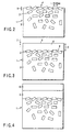
- FIG. 2 is a diagrammatic cross-sectional view of a substrate 1 having a semi-crystalline structure, such as PET.
- This structure may be understood as comprising numerous crystals 2 dispersed in random orientations within an amorphous bed 3.
- the crystals 2 have dimensions typically of the order of 10 to 20 nm.
- the degree of crystallinity depends on the polymer of the substrate 1.
- a typical value for PET and other polymers is around 30%, but may vary strongly depending on depth from the surface 4 and thermal and mechanical history approaching higher values at the surface, say, up to 70% and above.
- the crystals 2 embedded in the amorphous bed 3 protrude, creating roughness in the surface 4.
- the degree of roughness may be characterized by the Root Mean Square (RMS) roughness illustrated by the arrow 5.
- RMS roughness measured from AFM image for 1 ⁇ 1 ⁇ m 2 regions is about 1 to 2 nm.
- the surface roughness causes undesirable surface properties.
- the surface roughness is thought to play a negative roll when the substrate 1 is used for the deposition of further layers, for example of an inorganic glass coating, by causing defects and stresses in the further layer during its growth.
- the surface crystallinity hinders the diffusion of substances into the substrate.
- a layer 6 of polymer in an amorphous form is disposed on the surface of the substrate 1 to improve the surface properties, as illustrated in FIG. 3.
- the layer 6 covers the original surface 4 of the substrate, burying the crystals 2 protruding from the amorphous bed 3.
- the outer surface 8 of the layer is far flatter than the original surface 4 of the substrate 1 due to the uniform nature of amorphous material.
- the lower RMS roughness of the outer surface 8 is shown diagrammatically in FIG. 3 by the arrow 7.
- RMS roughness measured from AFM images for 1 ⁇ 1 ⁇ m 2 regions is about 0.2 to 0.4 nm (without annealing, as described below).
- the layer 6 improves the surface properties of the substrate 1. As the outer surface 8 is flatter, this assists in the deposition of further layers on top of the amorphous layer 6.
- the amorphous layer 6 is also softer and more adhesive. The amorphous nature of the material in the layer 6 assists in the diffusion of substances into the substrate 1.
- the crystalline structure of the crystals 2 protruding from the original surface 4 of the substrate 1 strengthens the amorphous layer 6 by providing a supportive framework.
- FIG. 4 is a diagrammatic cross-sectional view illustrating the treated substrate 1 shown in FIG. 3 with a further layer 10 deposited on the outer surface of the amorphous layer 6.
- the further layer 10 may comprise any material which it is desired to deposit on the substrate 1, for example an inorganic material such as metal, metal oxide, metalnitride, silicon oxide, silicon nitride, and the mixture thereof.
- the inorganic material may comprise SiO x (0 ⁇ x ⁇ 2), ITO (indium-tin oxide), TiO x (0 ⁇ x ⁇ 2), AlO x (0 ⁇ x ⁇ 1.5), MgO x (0 ⁇ x ⁇ 1), SnO x (0 ⁇ x ⁇ 1), ZrO x (0 ⁇ x ⁇ 2), and InO x (0 ⁇ x ⁇ 1).
- FIG. 4 is schematic.
- the further layer 10 may have any thickness whatsoever and is not restricted to having a thickness comparable with the amorphous layer 6.
- the layer 6 is desirably PET because this provides particularly advantageous surface properties.
- the layer 6 may be formed of any polymer selected to provide desired surface properties for the substrate 1, preferably a polyester, more preferably a polyalkylene terphthalate.
- the molecular weight of the layer 6 may take any value, although a molecular weight of at least around 15,000 is desirable.
- the present invention may be applied to a substrate of any polymer. Whilst the present invention is illustrated in FIG. 3 as applied to a substrate 1 having a semi-crystalline structure, in general the present invention may be applied to any substrate of polymer to improve its surface properties, preferably a polyester, more preferably a polyalkylene terphthalate.
- the substrate 1 may have any molecular weight suitable for good quality film formation (depending strongly on the polymer selected). For PET, a typical molecular weight would be in the range from around 15,000 to 60,000.
- the substrate 1 and the amorphous layer 6 are formed of substantially the same material to allow the surface properties of the substrate 1 to be improved without substantially changing the chemical and physical properties of the substrate 1 itself.
- the thickness of the layer 6 illustrate in FIG. 3 by the arrow 9 may have a wide range of values. At the lowermost end of the range, the thickness must simply be sufficient to improve the surface properties. Therefore, the thickness of the layer 6 must be sufficient to cover the crystals 2 protruding from the original surface 4 of the substrate 1. Therefore, in the case of a substrate 1 having a semi-crystalline structure including crystals 2 having dimensions of the order of 10 to 20 nm, it is desirable for the thickness of the layer 6 to be at least around 10 nm or more preferably around 20 nm.
- the thickness of the layer 6 As far as improving the surface properties of the substrate 1 is concerned, there is no absolute maximum limit on the thickness of the layer 6. However, there are other practical reasons why it is desirable to limit the thickness of the layer 6. For example, the mechanical strength of the layer 6 places a practical maximum on the thickness of the layer 6. The amorphous nature of the layer 6 causes it to have a relatively low mechanical strength, as compared to a substrate 1 have a semi-crystalline structure. For this reason, the maximum thickness of the layer 6 will be around 100 or 200 nm.
- a method of depositing the amorphous layer 6 on the substrate 1 will now be described.
- the method is principally to deposit a solution of the polymer of which the layer is to be formed onto the surface 4 of the substrate 1, accompanied by movement of the substrate 1 at a speed sufficient both to spread the solution over the substrate 1 and to evaporate the solvent, leaving a layer of the polymer in an amorphous form on the substrate 1.
- the method is performed as follows.
- a solution of the polymer that is to form the layer is prepared.
- Any solvent in which the polymer is soluble may be used, for example 2-chlorophenole.
- an amount of the solution is deposited on the surface 4 of the substrate 1.
- the substrate 1 is moved, preferably simultaneously with the deposition, at a speed sufficiently high as to spread the solution over the surface 4 of the substrate 1 and to evaporate the solvent.
- the method is based on an abrupt increase in the viscosity and solidification of the solution during the spreading and forced evaporation of the solvent under the influence of shear force applied to the solution as a result of the movement of the substrate 1.
- the viscosity of the solution depends on the solvent, the concentration of the solution.
- a typical concentration will be in the range from around 5 mg/ml to around 100 mg/ml, preferably from around 20 mg/ml to 50 mg/ml, depending on the molecular mass and chemical nature of the polymer in question and the molecular mass of the polymer.
- the speed of movement controls the rate of spreading, depending also on the viscosity of the solution.
- the speed of movement also controls the degree of evaporation, which depends also on the concentration of the solution.
- the amount of solution deposited and the speed of movement are then selected to spread the solution over a desired area, balanced against the concentration of the solution and its viscosity.
- the thickness of the deposited polymer can be controlled through the deposition speed and the solution concentration.
- the solution may be deposited on the surface 4 of the substrate 1 in discrete amounts or in a continuous process.
- One method is for the movement to be a rotation of the substrate 1.
- spreading of the solution is caused by the centrifugal force applied by the rotation of the substrate 1.
- a typical rotation speed range is from around 500 rpm to around 5,000 rmp. Best quality layers are formed with a speed range from around 1,000 rpm to around 3,000 rpm.
- the substrate 1 is moved linearly.
- a typical speed range is from around 2 m/s to around 20 m/s. Best quality layers are formed in the range from around 5 m/s to 10 m/s.
- the substrate 1 may be moved in a continuous process on an elongate substrate 1 with the solution being continuously deposited by injection onto the substrate 1.
- the present method is particularly suited to PET as a substrate 1 because of its low solubility in cold solvents in general.
- the method is performed at a temperature above around 10°C. Below that, there may be problems with adhesion and delamination due to mismatch of the elastic characteristics of the layer 6 and substrate 1 (at least during deposition due to the temperature gradient).
- the temperature is below the surface glass transition temperature of the layer (from around 50°C to 80°C for PET depending on the thickness of the layer 6), so a suggested temperature would be lower than around 45°C or 30°C.
- the layer 6 may be annealed with the purpose of increasing the crystallinity of the amorphous polymer.
- This is advantageous to increase the mechanical strength of the amorphous layer 6, although it is of course desirable to restrict the degree of crystallinity in the layer 6 to less than that of the substrate 1 so as to maintain the improvement in surface properties.
- the annealing occurs at a temperature above the glass transition temperature of the amorphous phase, for example, above 80°C for PET.
- the degree of crystallinity is controlled principally by the annealing temperature.
- the crystallinity may be controlled to have any value whatsoever, allowing variation from 0% when the layer 6 is initially formed up to, say, 70%. Crystallinity can also be controlled by thickness of the layer 6 and thermal history.
- the RMS roughness for a layer 6 of PET may be controlled up to, say, 3 nm as measured from an AFM image on a 1 ⁇ 1 ⁇ m 2 region.
- the method has been performed to deposit a layer of PET onto silicon and glass substrates.
- the method has been performed using an amount of 50 ⁇ l of a 1% wt. solution of PET in two-chlorophenole as a solvent.
- the substrate was moved by rotation at a spin rate in the range from 1000 to 3000 rpm. In this way, layers of thickness in the range from 180 nm and to 20 nm have been formed.
- the samples have been annealed at elevated temperatures, typically around 100 or 150°C.
- the resultant layers have been studied using AFM spectroscopy and Fourier transform infra-red (FTIR) spectroscopy.
- FTIR Fourier transform infra-red
- FIG. 5 an AFM image of an actual resultant PET layer is shown in FIG. 5, which has approximately the same scales as the AFM image of FIG. 1 and in which the PET layer has a thickness of about 80 nm.
- Analysis of such AFM images shows that the RMS roughness of the outer surface of the PET layer is significantly reduced below that of the PET film. This is clear, for example, from a comparison of the AFM images of FIGS. 1 and 5.
- AFM images show the layer as possessing an amorphous featureless structure.
Landscapes
- Chemical & Material Sciences (AREA)
- Health & Medical Sciences (AREA)
- Chemical Kinetics & Catalysis (AREA)
- Medicinal Chemistry (AREA)
- Polymers & Plastics (AREA)
- Organic Chemistry (AREA)
- Laminated Bodies (AREA)
- Treatments Of Macromolecular Shaped Articles (AREA)
- Graft Or Block Polymers (AREA)
- Coating Of Shaped Articles Made Of Macromolecular Substances (AREA)
- Physical Vapour Deposition (AREA)
Abstract
Description
The inorganic material may comprise SiOx (0 ≦ x ≦ 2), ITO (indium-tin oxide), TiOx (0 ≦ x ≦ 2), AlOx (0 ≦ x ≦ 1.5), MgOx (0 ≦ x ≦ 1), SnOx (0 ≦ x ≦ 1), ZrOx (0 ≦ x ≦ 2), and InOx (0 ≦ x ≦ 1). As regards the thickness of the
Claims (26)
- A substrate comprising:a first polymer; anda layer comprising a second polymer in an amorphous form disposed on a surface of the first polymer.
- The substrate according to claim 1, wherein the second polymer comprises polyethylene terphthalate.
- The substrate according to claim 1, wherein the first polymer has a semi-crystalline structure.
- The substrate according to claim 1, wherein the first and second polymers are the same material.
- The substrate according to claim 3, wherein the second polymer comprises polyethylene terphthalate.
- The substrate according to claim 3, wherein the first polymer comprises polyethylene terphathalate.
- The substrate according to claim 1, wherein the second polymer has a degree of crystallinity less than that of the first polymer.
- The substrate according to claim 1, wherein the layer is solution-cast.
- The substrate according to claim 1, wherein the thickness of the layer is around 200 nm or below.
- The substrate according to claim 1, wherein the thickness of the layer is around 10 nm or above.
- The substrate according to claim 1, further comprising at least one further layer disposed on the layer of the second polymer.
- The substrate according to claim 1, further comprising a further layer disposed on the layer comprising the second polymer.
- The substrate according to claim 12, wherein the further layer comprises an inorganic material.
- The substrate according to claim 13, wherein the further layer comprises glass.
- A method of depositing, on a substrate comprising a first polymer, a layer comprising a second polymer in an amorphous form, comprising:preparing a solution of the second polymer in a solvent;depositing an amount of the solution on a surface of the substrate; andmoving the substrate at a speed sufficient both to spread the solution over the surface of the substrate and to evaporate the solvent, thereby leaving the layer of the second polymer in an amorphous form on the substrate.
- The method according to claim 15, wherein the steps of depositing and moving are performed simultaneously.
- The method according to claim 15, wherein the steps of depositing and moving comprise rotating the substrate.
- The method according to claim 17, wherein the substrate is rotated at a speed in the range from around 500 rpm to 5000 rpm.
- The method according to claim 15, further comprising the step of annealing the layer at a temperature sufficient to increase the crystallinity of the second polymer.
- The method according to claim 15, wherein the step of moving the substrate comprises rotating the substrate.
- The method according to claim 15, wherein the first polymer has a semi-crystalline structure.
- The method according to claim 15, wherein the second polymer comprises polyethylene terphathalate.
- The method according to claim 15, wherein the substrate comprises polyethylene terphathalate.
- The method according to claim 15, wherein the first and second polymers are of the same material.
- The substrate having, disposed on a surface thereof, a layer comprising a polymer substantially as hereinbefore described with reference to FIGS. 3 to 5 of the accompanying drawings.
- The method of depositing a layer comprising a polymer on a substrate, substantially as hereinbefore described with reference of FIGS. 3 to 5 of the accompanying drawings.
Applications Claiming Priority (3)
| Application Number | Priority Date | Filing Date | Title |
|---|---|---|---|
| GB0027432 | 2000-11-09 | ||
| GB0027432A GB2368810A (en) | 2000-11-09 | 2000-11-09 | Treatment of a surface of a polymer |
| PCT/JP2001/009726 WO2002038380A1 (en) | 2000-11-09 | 2001-11-07 | Surface treating of polymer |
Publications (3)
| Publication Number | Publication Date |
|---|---|
| EP1270204A1 true EP1270204A1 (en) | 2003-01-02 |
| EP1270204A4 EP1270204A4 (en) | 2003-03-26 |
| EP1270204B1 EP1270204B1 (en) | 2006-05-17 |
Family
ID=9902908
Family Applications (1)
| Application Number | Title | Priority Date | Filing Date |
|---|---|---|---|
| EP01981002A Expired - Lifetime EP1270204B1 (en) | 2000-11-09 | 2001-11-07 | Surface treating of polymer |
Country Status (7)
| Country | Link |
|---|---|
| US (1) | US20030008136A1 (en) |
| EP (1) | EP1270204B1 (en) |
| JP (1) | JP4036095B2 (en) |
| AT (1) | ATE326336T1 (en) |
| DE (1) | DE60119712T2 (en) |
| GB (1) | GB2368810A (en) |
| WO (1) | WO2002038380A1 (en) |
Families Citing this family (9)
| Publication number | Priority date | Publication date | Assignee | Title |
|---|---|---|---|---|
| JP3692096B2 (en) * | 2002-06-28 | 2005-09-07 | ニスカ株式会社 | ND filter, manufacturing method thereof, and diaphragm device incorporating the ND filter |
| US20110200844A1 (en) * | 2010-02-17 | 2011-08-18 | Frito-Lay North America, Inc. | Composition for facilitating environmental degradation of a film |
| US9040120B2 (en) | 2011-08-05 | 2015-05-26 | Frito-Lay North America, Inc. | Inorganic nanocoating primed organic film |
| US20130101831A1 (en) * | 2011-10-20 | 2013-04-25 | Frito-Lay North America, Inc. | Metallized paper packaging film and process for its production |
| US9267011B2 (en) | 2012-03-20 | 2016-02-23 | Frito-Lay North America, Inc. | Composition and method for making a cavitated bio-based film |
| US9162421B2 (en) | 2012-04-25 | 2015-10-20 | Frito-Lay North America, Inc. | Film with compostable heat seal layer |
| US9284104B2 (en) | 2012-06-23 | 2016-03-15 | Frito-Lay North America, Inc. | Deposition of ultra-thin inorganic oxide coatings on packaging |
| US9090021B2 (en) | 2012-08-02 | 2015-07-28 | Frito-Lay North America, Inc. | Ultrasonic sealing of packages |
| US9149980B2 (en) | 2012-08-02 | 2015-10-06 | Frito-Lay North America, Inc. | Ultrasonic sealing of packages |
Family Cites Families (26)
| Publication number | Priority date | Publication date | Assignee | Title |
|---|---|---|---|---|
| JPS5028118B2 (en) * | 1971-08-14 | 1975-09-12 | ||
| US3871947A (en) * | 1973-01-15 | 1975-03-18 | Minnesota Mining & Mfg | Biaxially oriented polyethylene terephthalate film having a surface suitable for writing thereon |
| US4275113A (en) * | 1978-10-17 | 1981-06-23 | Hitachi Maxell, Ltd. | Magnetic recording medium |
| JPS58147353A (en) * | 1982-02-26 | 1983-09-02 | 日本板硝子株式会社 | Laminated panel |
| JPS5919230A (en) * | 1982-07-21 | 1984-01-31 | Fuji Photo Film Co Ltd | Magnetic recording medium |
| GB8925785D0 (en) * | 1989-11-15 | 1990-01-04 | Ici Plc | Multilayer film |
| US5405663A (en) * | 1991-11-12 | 1995-04-11 | Hunt-Wesson, Inc. | Microwave package laminate with extrusion bonded susceptor |
| JPH05212840A (en) * | 1992-02-04 | 1993-08-24 | Ajinomoto Co Inc | Heat-sealable polyester sheet |
| US5626942A (en) * | 1993-05-05 | 1997-05-06 | Toray Industries, Inc. | Polyester film and process for producing the same |
| JPH07268189A (en) * | 1994-03-30 | 1995-10-17 | Teijin Ltd | Polyester water dispersion and polyester film |
| MY113596A (en) * | 1995-04-11 | 2002-04-30 | Daicel Chem | Barrier composite films and method of producing the same |
| WO1997037053A1 (en) * | 1996-04-01 | 1997-10-09 | Mobil Oil Corporation | Barrier films having vapor coated high energy surfaces |
| JPH1076593A (en) * | 1996-09-03 | 1998-03-24 | Daicel Chem Ind Ltd | Barrier composite film and its manufacture |
| US5919878A (en) * | 1996-09-13 | 1999-07-06 | E. I. Du Pont De Nemours And Company | Amorphous fluoropolymer containing perfluoro(ethyl vinyl ether) |
| JPH10250015A (en) * | 1997-03-13 | 1998-09-22 | Toyobo Co Ltd | Polyester laminated sheet and molded article thereof |
| JP3589833B2 (en) * | 1997-06-30 | 2004-11-17 | 三菱樹脂株式会社 | Silicone rubber composite |
| JPH1160756A (en) * | 1997-08-12 | 1999-03-05 | Toray Ind Inc | Liquid crystalline polyester film and method for producing the same |
| DE19741878A1 (en) * | 1997-09-23 | 1999-03-25 | Hoechst Diafoil Gmbh | Multi-layer, biaxially oriented polyester film, process for its production and its use |
| DE19813269A1 (en) * | 1998-03-25 | 1999-09-30 | Hoechst Diafoil Gmbh | Sealable polyester film with high oxygen barrier, process for its production and its use |
| DE19834603A1 (en) * | 1998-07-31 | 2000-02-03 | Hoechst Diafoil Gmbh | Matte, co-extruded polyester film, process for its production and its use |
| JP2000153594A (en) * | 1998-11-20 | 2000-06-06 | Unitika Ltd | Two-layered polyester resin sheet, polyester resin laminate using the same, and production thereof |
| DE10002150A1 (en) * | 2000-01-20 | 2001-07-26 | Mitsubishi Polyester Film Gmbh | Amorphous white sealable polyester film, useful for labels and protective screens, comprises a base layer having layers coated either side containing a UV-stabilizer and a flame retardant. |
| DE10002149A1 (en) * | 2000-01-20 | 2001-07-26 | Mitsubishi Polyester Film Gmbh | Amorphous transparent sealable polyester film, useful for labels and protective screens, comprises a base layer having layers coated either side containing a UV-stabilizer and a flame retardant |
| DE10002170A1 (en) * | 2000-01-20 | 2001-07-26 | Mitsubishi Polyester Film Gmbh | Amorphous, thermoformable, UV-stabilized, flame retardant polyester film, useful in interior or exterior applications, comprising base layer with sealable and matt covering layers |
| JP2001260152A (en) * | 2000-03-21 | 2001-09-25 | Kanegafuchi Chem Ind Co Ltd | Optical film manufacturing method |
| JP2001307945A (en) * | 2000-04-21 | 2001-11-02 | Toyobo Co Ltd | Polyester film for condenser and roll-up condenser using the same |
-
2000
- 2000-11-09 GB GB0027432A patent/GB2368810A/en not_active Withdrawn
-
2001
- 2001-11-07 AT AT01981002T patent/ATE326336T1/en not_active IP Right Cessation
- 2001-11-07 DE DE60119712T patent/DE60119712T2/en not_active Expired - Lifetime
- 2001-11-07 WO PCT/JP2001/009726 patent/WO2002038380A1/en not_active Ceased
- 2001-11-07 EP EP01981002A patent/EP1270204B1/en not_active Expired - Lifetime
- 2001-11-07 JP JP2002540936A patent/JP4036095B2/en not_active Expired - Fee Related
-
2002
- 2002-08-20 US US10/223,469 patent/US20030008136A1/en not_active Abandoned
Also Published As
| Publication number | Publication date |
|---|---|
| JPWO2002038380A1 (en) | 2004-03-11 |
| GB0027432D0 (en) | 2000-12-27 |
| ATE326336T1 (en) | 2006-06-15 |
| DE60119712T2 (en) | 2006-10-19 |
| GB2368810A (en) | 2002-05-15 |
| JP4036095B2 (en) | 2008-01-23 |
| EP1270204A4 (en) | 2003-03-26 |
| WO2002038380A1 (en) | 2002-05-16 |
| EP1270204B1 (en) | 2006-05-17 |
| US20030008136A1 (en) | 2003-01-09 |
| DE60119712D1 (en) | 2006-06-22 |
Similar Documents
| Publication | Publication Date | Title |
|---|---|---|
| Teshima et al. | Transparent ultra water-repellent poly (ethylene terephthalate) substrates fabricated by oxygen plasma treatment and subsequent hydrophobic coating | |
| EP1270204B1 (en) | Surface treating of polymer | |
| Semaltianos | Thermally evaporated aluminium thin films | |
| FR2800731A1 (en) | TRANSPARENT SUBSTRATE WITH SILICON DERIVED LAYER | |
| CN103290394B (en) | A kind of surface treatment method of the metal base band for the preparation of s-generation high temperature superconducting materia | |
| Seveno et al. | Preparation of multi-coating PZT thick films by sol–gel method onto stainless steel substrates | |
| US6821338B2 (en) | Particle beam biaxial orientation of a substrate for epitaxial crystal growth | |
| Gao et al. | Preparation of SrTiO3 thin films by the liquid phase deposition method | |
| Fu et al. | Preparation and characterization of MgO thin films by a novel sol-gel method | |
| US20030019668A1 (en) | Particle beam biaxial orientation of a substrate for epitaxial crystal growth | |
| Mandal et al. | Control of Ferroelectricity in Solution‐Processed Hafnia Films Through Annealing Atmosphere | |
| Chu et al. | Surface engineering of the flexible metallic substrate by SDP‐Gd‐Zr‐O layer for IBAD‐MgO templates | |
| Zhang et al. | Partial dewetting of polyethylene thin films on rough silicon dioxide surfaces | |
| Bouquet et al. | Structural and surface morphology characterizations of oriented LiNbO3 thin films grown by polymeric precursor method | |
| Rai et al. | Wet oxidation of amorphous Si‐Ge layer deposited on Si (001) at 800 and 900° C | |
| Zhu et al. | Orientation of MgO thin films grown by pulsed laser deposition | |
| Zhu et al. | Growth of SrTiO3 thin films on BaxSr1− xTiO3 (x= 0.3, 0.5) seed layers on Ni (2 0 0) substrates using spin coating technique | |
| Sukjit et al. | Size-dependent and spatial variations in the structural properties of spin-coated poly (Vinylidene Fluoride) films | |
| CN1741253A (en) | Preparation method of single-oriented ferroelectric thin film with biaxially textured MgO as buffer layer | |
| CN118621448B (en) | A method for preparing large-area single-layer single-crystal domain organic semiconductor single crystal | |
| Kondo et al. | Nanoscale polydiacetylene wire structures prepared by molecular beam deposition on semiconductor substrates | |
| Nakamura et al. | Preparation of titanium dioxide thin films by means of a hot wall technique | |
| Oh et al. | Direct deposition of silica films using silicon alkoxide solution | |
| Khairuddin | Investigation of crystal growth observed in crystallization in thin polyethtlene therethalate film | |
| Rousseau et al. | CeO2 epitaxial films by spray MOD |
Legal Events
| Date | Code | Title | Description |
|---|---|---|---|
| PUAI | Public reference made under article 153(3) epc to a published international application that has entered the european phase |
Free format text: ORIGINAL CODE: 0009012 |
|
| 17P | Request for examination filed |
Effective date: 20020807 |
|
| AK | Designated contracting states |
Kind code of ref document: A1 Designated state(s): AT BE CH CY DE DK ES FI FR GB GR IE IT LI LU MC NL PT SE TR |
|
| A4 | Supplementary search report drawn up and despatched |
Effective date: 20030210 |
|
| RIC1 | Information provided on ipc code assigned before grant |
Ipc: 7B 32B 27/36 B Ipc: 7B 32B 5/14 B Ipc: 7B 32B 27/00 A Ipc: 7C 08J 7/04 B Ipc: 7B 32B 7/02 B |
|
| 17Q | First examination report despatched |
Effective date: 20050317 |
|
| GRAP | Despatch of communication of intention to grant a patent |
Free format text: ORIGINAL CODE: EPIDOSNIGR1 |
|
| GRAS | Grant fee paid |
Free format text: ORIGINAL CODE: EPIDOSNIGR3 |
|
| GRAA | (expected) grant |
Free format text: ORIGINAL CODE: 0009210 |
|
| AK | Designated contracting states |
Kind code of ref document: B1 Designated state(s): AT BE CH CY DE DK ES FI FR GB GR IE IT LI LU MC NL PT SE TR |
|
| PG25 | Lapsed in a contracting state [announced via postgrant information from national office to epo] |
Ref country code: IT Free format text: LAPSE BECAUSE OF FAILURE TO SUBMIT A TRANSLATION OF THE DESCRIPTION OR TO PAY THE FEE WITHIN THE PRESCRIBED TIME-LIMIT;WARNING: LAPSES OF ITALIAN PATENTS WITH EFFECTIVE DATE BEFORE 2007 MAY HAVE OCCURRED AT ANY TIME BEFORE 2007. THE CORRECT EFFECTIVE DATE MAY BE DIFFERENT FROM THE ONE RECORDED. Effective date: 20060517 Ref country code: LI Free format text: LAPSE BECAUSE OF FAILURE TO SUBMIT A TRANSLATION OF THE DESCRIPTION OR TO PAY THE FEE WITHIN THE PRESCRIBED TIME-LIMIT Effective date: 20060517 Ref country code: CH Free format text: LAPSE BECAUSE OF FAILURE TO SUBMIT A TRANSLATION OF THE DESCRIPTION OR TO PAY THE FEE WITHIN THE PRESCRIBED TIME-LIMIT Effective date: 20060517 Ref country code: BE Free format text: LAPSE BECAUSE OF FAILURE TO SUBMIT A TRANSLATION OF THE DESCRIPTION OR TO PAY THE FEE WITHIN THE PRESCRIBED TIME-LIMIT Effective date: 20060517 Ref country code: AT Free format text: LAPSE BECAUSE OF FAILURE TO SUBMIT A TRANSLATION OF THE DESCRIPTION OR TO PAY THE FEE WITHIN THE PRESCRIBED TIME-LIMIT Effective date: 20060517 Ref country code: NL Free format text: LAPSE BECAUSE OF FAILURE TO SUBMIT A TRANSLATION OF THE DESCRIPTION OR TO PAY THE FEE WITHIN THE PRESCRIBED TIME-LIMIT Effective date: 20060517 Ref country code: FI Free format text: LAPSE BECAUSE OF FAILURE TO SUBMIT A TRANSLATION OF THE DESCRIPTION OR TO PAY THE FEE WITHIN THE PRESCRIBED TIME-LIMIT Effective date: 20060517 |
|
| REG | Reference to a national code |
Ref country code: GB Ref legal event code: FG4D |
|
| REG | Reference to a national code |
Ref country code: CH Ref legal event code: EP |
|
| REG | Reference to a national code |
Ref country code: IE Ref legal event code: FG4D |
|
| REF | Corresponds to: |
Ref document number: 60119712 Country of ref document: DE Date of ref document: 20060622 Kind code of ref document: P |
|
| PG25 | Lapsed in a contracting state [announced via postgrant information from national office to epo] |
Ref country code: SE Free format text: LAPSE BECAUSE OF FAILURE TO SUBMIT A TRANSLATION OF THE DESCRIPTION OR TO PAY THE FEE WITHIN THE PRESCRIBED TIME-LIMIT Effective date: 20060817 Ref country code: DK Free format text: LAPSE BECAUSE OF FAILURE TO SUBMIT A TRANSLATION OF THE DESCRIPTION OR TO PAY THE FEE WITHIN THE PRESCRIBED TIME-LIMIT Effective date: 20060817 |
|
| PG25 | Lapsed in a contracting state [announced via postgrant information from national office to epo] |
Ref country code: ES Free format text: LAPSE BECAUSE OF FAILURE TO SUBMIT A TRANSLATION OF THE DESCRIPTION OR TO PAY THE FEE WITHIN THE PRESCRIBED TIME-LIMIT Effective date: 20060828 |
|
| PG25 | Lapsed in a contracting state [announced via postgrant information from national office to epo] |
Ref country code: PT Free format text: LAPSE BECAUSE OF FAILURE TO SUBMIT A TRANSLATION OF THE DESCRIPTION OR TO PAY THE FEE WITHIN THE PRESCRIBED TIME-LIMIT Effective date: 20061017 |
|
| NLV1 | Nl: lapsed or annulled due to failure to fulfill the requirements of art. 29p and 29m of the patents act | ||
| PG25 | Lapsed in a contracting state [announced via postgrant information from national office to epo] |
Ref country code: IE Free format text: LAPSE BECAUSE OF NON-PAYMENT OF DUE FEES Effective date: 20061107 |
|
| PG25 | Lapsed in a contracting state [announced via postgrant information from national office to epo] |
Ref country code: MC Free format text: LAPSE BECAUSE OF NON-PAYMENT OF DUE FEES Effective date: 20061130 |
|
| REG | Reference to a national code |
Ref country code: CH Ref legal event code: PL |
|
| ET | Fr: translation filed | ||
| PLBE | No opposition filed within time limit |
Free format text: ORIGINAL CODE: 0009261 |
|
| STAA | Information on the status of an ep patent application or granted ep patent |
Free format text: STATUS: NO OPPOSITION FILED WITHIN TIME LIMIT |
|
| 26N | No opposition filed |
Effective date: 20070220 |
|
| PG25 | Lapsed in a contracting state [announced via postgrant information from national office to epo] |
Ref country code: GR Free format text: LAPSE BECAUSE OF FAILURE TO SUBMIT A TRANSLATION OF THE DESCRIPTION OR TO PAY THE FEE WITHIN THE PRESCRIBED TIME-LIMIT Effective date: 20060818 |
|
| PG25 | Lapsed in a contracting state [announced via postgrant information from national office to epo] |
Ref country code: TR Free format text: LAPSE BECAUSE OF FAILURE TO SUBMIT A TRANSLATION OF THE DESCRIPTION OR TO PAY THE FEE WITHIN THE PRESCRIBED TIME-LIMIT Effective date: 20060517 Ref country code: LU Free format text: LAPSE BECAUSE OF NON-PAYMENT OF DUE FEES Effective date: 20061107 |
|
| PG25 | Lapsed in a contracting state [announced via postgrant information from national office to epo] |
Ref country code: CY Free format text: LAPSE BECAUSE OF FAILURE TO SUBMIT A TRANSLATION OF THE DESCRIPTION OR TO PAY THE FEE WITHIN THE PRESCRIBED TIME-LIMIT Effective date: 20060517 |
|
| PGFP | Annual fee paid to national office [announced via postgrant information from national office to epo] |
Ref country code: GB Payment date: 20131125 Year of fee payment: 13 Ref country code: DE Payment date: 20131126 Year of fee payment: 13 |
|
| PGFP | Annual fee paid to national office [announced via postgrant information from national office to epo] |
Ref country code: FR Payment date: 20131202 Year of fee payment: 13 |
|
| REG | Reference to a national code |
Ref country code: DE Ref legal event code: R119 Ref document number: 60119712 Country of ref document: DE |
|
| GBPC | Gb: european patent ceased through non-payment of renewal fee |
Effective date: 20141107 |
|
| REG | Reference to a national code |
Ref country code: FR Ref legal event code: ST Effective date: 20150731 |
|
| PG25 | Lapsed in a contracting state [announced via postgrant information from national office to epo] |
Ref country code: GB Free format text: LAPSE BECAUSE OF NON-PAYMENT OF DUE FEES Effective date: 20141107 Ref country code: DE Free format text: LAPSE BECAUSE OF NON-PAYMENT OF DUE FEES Effective date: 20150602 |
|
| PG25 | Lapsed in a contracting state [announced via postgrant information from national office to epo] |
Ref country code: FR Free format text: LAPSE BECAUSE OF NON-PAYMENT OF DUE FEES Effective date: 20141201 |