EP1267402A2 - Dispositif semi-conducteur et méthode de fabrication associée - Google Patents
Dispositif semi-conducteur et méthode de fabrication associée Download PDFInfo
- Publication number
- EP1267402A2 EP1267402A2 EP02291419A EP02291419A EP1267402A2 EP 1267402 A2 EP1267402 A2 EP 1267402A2 EP 02291419 A EP02291419 A EP 02291419A EP 02291419 A EP02291419 A EP 02291419A EP 1267402 A2 EP1267402 A2 EP 1267402A2
- Authority
- EP
- European Patent Office
- Prior art keywords
- electrode pad
- semiconductor
- hole
- semiconductor device
- opening
- Prior art date
- Legal status (The legal status is an assumption and is not a legal conclusion. Google has not performed a legal analysis and makes no representation as to the accuracy of the status listed.)
- Granted
Links
- 239000004065 semiconductor Substances 0.000 title claims abstract description 184
- 238000000034 method Methods 0.000 title claims description 26
- 238000004519 manufacturing process Methods 0.000 title claims description 14
- 239000000758 substrate Substances 0.000 claims abstract description 111
- 239000004020 conductor Substances 0.000 claims description 23
- 238000010304 firing Methods 0.000 claims description 9
- 238000000059 patterning Methods 0.000 claims description 9
- 238000005498 polishing Methods 0.000 claims description 3
- 229910052710 silicon Inorganic materials 0.000 abstract description 48
- 239000010703 silicon Substances 0.000 abstract description 48
- XUIMIQQOPSSXEZ-UHFFFAOYSA-N Silicon Chemical compound [Si] XUIMIQQOPSSXEZ-UHFFFAOYSA-N 0.000 abstract description 46
- VYPSYNLAJGMNEJ-UHFFFAOYSA-N Silicium dioxide Chemical compound O=[Si]=O VYPSYNLAJGMNEJ-UHFFFAOYSA-N 0.000 abstract description 44
- 229910052681 coesite Inorganic materials 0.000 abstract description 22
- 229910052906 cristobalite Inorganic materials 0.000 abstract description 22
- 239000000377 silicon dioxide Substances 0.000 abstract description 22
- 229910052682 stishovite Inorganic materials 0.000 abstract description 22
- 229910052905 tridymite Inorganic materials 0.000 abstract description 22
- 230000015572 biosynthetic process Effects 0.000 abstract description 17
- 239000010949 copper Substances 0.000 description 15
- RYGMFSIKBFXOCR-UHFFFAOYSA-N Copper Chemical compound [Cu] RYGMFSIKBFXOCR-UHFFFAOYSA-N 0.000 description 14
- 229910052802 copper Inorganic materials 0.000 description 14
- 229910000679 solder Inorganic materials 0.000 description 13
- 238000002161 passivation Methods 0.000 description 9
- 238000009413 insulation Methods 0.000 description 8
- 229920002120 photoresistant polymer Polymers 0.000 description 7
- 229910052782 aluminium Inorganic materials 0.000 description 6
- XAGFODPZIPBFFR-UHFFFAOYSA-N aluminium Chemical compound [Al] XAGFODPZIPBFFR-UHFFFAOYSA-N 0.000 description 6
- VYZAMTAEIAYCRO-UHFFFAOYSA-N Chromium Chemical compound [Cr] VYZAMTAEIAYCRO-UHFFFAOYSA-N 0.000 description 5
- 239000000463 material Substances 0.000 description 5
- 238000004544 sputter deposition Methods 0.000 description 5
- 238000005229 chemical vapour deposition Methods 0.000 description 4
- 238000000151 deposition Methods 0.000 description 4
- 230000008016 vaporization Effects 0.000 description 4
- 238000005530 etching Methods 0.000 description 3
- PXHVJJICTQNCMI-UHFFFAOYSA-N nickel Substances [Ni] PXHVJJICTQNCMI-UHFFFAOYSA-N 0.000 description 3
- 238000007747 plating Methods 0.000 description 3
- 230000001681 protective effect Effects 0.000 description 3
- 238000003486 chemical etching Methods 0.000 description 2
- 238000004140 cleaning Methods 0.000 description 2
- 239000010931 gold Substances 0.000 description 2
- 238000001020 plasma etching Methods 0.000 description 2
- 150000003376 silicon Chemical class 0.000 description 2
- 239000011364 vaporized material Substances 0.000 description 2
- 230000008021 deposition Effects 0.000 description 1
- 230000000694 effects Effects 0.000 description 1
- 238000009713 electroplating Methods 0.000 description 1
- PCHJSUWPFVWCPO-UHFFFAOYSA-N gold Chemical compound [Au] PCHJSUWPFVWCPO-UHFFFAOYSA-N 0.000 description 1
- 229910052737 gold Inorganic materials 0.000 description 1
- 229910052751 metal Inorganic materials 0.000 description 1
- 239000002184 metal Substances 0.000 description 1
- 238000012986 modification Methods 0.000 description 1
- 230000004048 modification Effects 0.000 description 1
- 229910052759 nickel Inorganic materials 0.000 description 1
- 239000000126 substance Substances 0.000 description 1
- 238000009834 vaporization Methods 0.000 description 1
- 238000005406 washing Methods 0.000 description 1
Images


Classifications
-
- H—ELECTRICITY
- H01—ELECTRIC ELEMENTS
- H01L—SEMICONDUCTOR DEVICES NOT COVERED BY CLASS H10
- H01L21/00—Processes or apparatus adapted for the manufacture or treatment of semiconductor or solid state devices or of parts thereof
- H01L21/70—Manufacture or treatment of devices consisting of a plurality of solid state components formed in or on a common substrate or of parts thereof; Manufacture of integrated circuit devices or of parts thereof
- H01L21/71—Manufacture of specific parts of devices defined in group H01L21/70
- H01L21/768—Applying interconnections to be used for carrying current between separate components within a device comprising conductors and dielectrics
- H01L21/76898—Applying interconnections to be used for carrying current between separate components within a device comprising conductors and dielectrics formed through a semiconductor substrate
-
- H—ELECTRICITY
- H01—ELECTRIC ELEMENTS
- H01L—SEMICONDUCTOR DEVICES NOT COVERED BY CLASS H10
- H01L23/00—Details of semiconductor or other solid state devices
- H01L23/48—Arrangements for conducting electric current to or from the solid state body in operation, e.g. leads, terminal arrangements ; Selection of materials therefor
- H01L23/481—Internal lead connections, e.g. via connections, feedthrough structures
-
- H—ELECTRICITY
- H01—ELECTRIC ELEMENTS
- H01L—SEMICONDUCTOR DEVICES NOT COVERED BY CLASS H10
- H01L25/00—Assemblies consisting of a plurality of individual semiconductor or other solid state devices ; Multistep manufacturing processes thereof
- H01L25/03—Assemblies consisting of a plurality of individual semiconductor or other solid state devices ; Multistep manufacturing processes thereof all the devices being of a type provided for in the same subgroup of groups H01L27/00 - H01L33/00, or in a single subclass of H10K, H10N, e.g. assemblies of rectifier diodes
- H01L25/04—Assemblies consisting of a plurality of individual semiconductor or other solid state devices ; Multistep manufacturing processes thereof all the devices being of a type provided for in the same subgroup of groups H01L27/00 - H01L33/00, or in a single subclass of H10K, H10N, e.g. assemblies of rectifier diodes the devices not having separate containers
- H01L25/065—Assemblies consisting of a plurality of individual semiconductor or other solid state devices ; Multistep manufacturing processes thereof all the devices being of a type provided for in the same subgroup of groups H01L27/00 - H01L33/00, or in a single subclass of H10K, H10N, e.g. assemblies of rectifier diodes the devices not having separate containers the devices being of a type provided for in group H01L27/00
- H01L25/0657—Stacked arrangements of devices
-
- H—ELECTRICITY
- H01—ELECTRIC ELEMENTS
- H01L—SEMICONDUCTOR DEVICES NOT COVERED BY CLASS H10
- H01L25/00—Assemblies consisting of a plurality of individual semiconductor or other solid state devices ; Multistep manufacturing processes thereof
- H01L25/50—Multistep manufacturing processes of assemblies consisting of devices, each device being of a type provided for in group H01L27/00 or H01L29/00
-
- H—ELECTRICITY
- H01—ELECTRIC ELEMENTS
- H01L—SEMICONDUCTOR DEVICES NOT COVERED BY CLASS H10
- H01L2224/00—Indexing scheme for arrangements for connecting or disconnecting semiconductor or solid-state bodies and methods related thereto as covered by H01L24/00
- H01L2224/01—Means for bonding being attached to, or being formed on, the surface to be connected, e.g. chip-to-package, die-attach, "first-level" interconnects; Manufacturing methods related thereto
- H01L2224/02—Bonding areas; Manufacturing methods related thereto
- H01L2224/023—Redistribution layers [RDL] for bonding areas
- H01L2224/0237—Disposition of the redistribution layers
- H01L2224/02371—Disposition of the redistribution layers connecting the bonding area on a surface of the semiconductor or solid-state body with another surface of the semiconductor or solid-state body
-
- H—ELECTRICITY
- H01—ELECTRIC ELEMENTS
- H01L—SEMICONDUCTOR DEVICES NOT COVERED BY CLASS H10
- H01L2224/00—Indexing scheme for arrangements for connecting or disconnecting semiconductor or solid-state bodies and methods related thereto as covered by H01L24/00
- H01L2224/01—Means for bonding being attached to, or being formed on, the surface to be connected, e.g. chip-to-package, die-attach, "first-level" interconnects; Manufacturing methods related thereto
- H01L2224/02—Bonding areas; Manufacturing methods related thereto
- H01L2224/023—Redistribution layers [RDL] for bonding areas
- H01L2224/0237—Disposition of the redistribution layers
- H01L2224/02377—Fan-in arrangement
-
- H—ELECTRICITY
- H01—ELECTRIC ELEMENTS
- H01L—SEMICONDUCTOR DEVICES NOT COVERED BY CLASS H10
- H01L2224/00—Indexing scheme for arrangements for connecting or disconnecting semiconductor or solid-state bodies and methods related thereto as covered by H01L24/00
- H01L2224/01—Means for bonding being attached to, or being formed on, the surface to be connected, e.g. chip-to-package, die-attach, "first-level" interconnects; Manufacturing methods related thereto
- H01L2224/02—Bonding areas; Manufacturing methods related thereto
- H01L2224/04—Structure, shape, material or disposition of the bonding areas prior to the connecting process
- H01L2224/05—Structure, shape, material or disposition of the bonding areas prior to the connecting process of an individual bonding area
- H01L2224/05001—Internal layers
- H01L2224/05005—Structure
- H01L2224/05009—Bonding area integrally formed with a via connection of the semiconductor or solid-state body
-
- H—ELECTRICITY
- H01—ELECTRIC ELEMENTS
- H01L—SEMICONDUCTOR DEVICES NOT COVERED BY CLASS H10
- H01L2224/00—Indexing scheme for arrangements for connecting or disconnecting semiconductor or solid-state bodies and methods related thereto as covered by H01L24/00
- H01L2224/01—Means for bonding being attached to, or being formed on, the surface to be connected, e.g. chip-to-package, die-attach, "first-level" interconnects; Manufacturing methods related thereto
- H01L2224/02—Bonding areas; Manufacturing methods related thereto
- H01L2224/04—Structure, shape, material or disposition of the bonding areas prior to the connecting process
- H01L2224/05—Structure, shape, material or disposition of the bonding areas prior to the connecting process of an individual bonding area
- H01L2224/05001—Internal layers
- H01L2224/0502—Disposition
- H01L2224/05023—Disposition the whole internal layer protruding from the surface
-
- H—ELECTRICITY
- H01—ELECTRIC ELEMENTS
- H01L—SEMICONDUCTOR DEVICES NOT COVERED BY CLASS H10
- H01L2224/00—Indexing scheme for arrangements for connecting or disconnecting semiconductor or solid-state bodies and methods related thereto as covered by H01L24/00
- H01L2224/01—Means for bonding being attached to, or being formed on, the surface to be connected, e.g. chip-to-package, die-attach, "first-level" interconnects; Manufacturing methods related thereto
- H01L2224/02—Bonding areas; Manufacturing methods related thereto
- H01L2224/04—Structure, shape, material or disposition of the bonding areas prior to the connecting process
- H01L2224/05—Structure, shape, material or disposition of the bonding areas prior to the connecting process of an individual bonding area
- H01L2224/05001—Internal layers
- H01L2224/0502—Disposition
- H01L2224/05025—Disposition the internal layer being disposed on a via connection of the semiconductor or solid-state body
-
- H—ELECTRICITY
- H01—ELECTRIC ELEMENTS
- H01L—SEMICONDUCTOR DEVICES NOT COVERED BY CLASS H10
- H01L2224/00—Indexing scheme for arrangements for connecting or disconnecting semiconductor or solid-state bodies and methods related thereto as covered by H01L24/00
- H01L2224/01—Means for bonding being attached to, or being formed on, the surface to be connected, e.g. chip-to-package, die-attach, "first-level" interconnects; Manufacturing methods related thereto
- H01L2224/02—Bonding areas; Manufacturing methods related thereto
- H01L2224/04—Structure, shape, material or disposition of the bonding areas prior to the connecting process
- H01L2224/05—Structure, shape, material or disposition of the bonding areas prior to the connecting process of an individual bonding area
- H01L2224/0554—External layer
- H01L2224/0556—Disposition
- H01L2224/0557—Disposition the external layer being disposed on a via connection of the semiconductor or solid-state body
-
- H—ELECTRICITY
- H01—ELECTRIC ELEMENTS
- H01L—SEMICONDUCTOR DEVICES NOT COVERED BY CLASS H10
- H01L2224/00—Indexing scheme for arrangements for connecting or disconnecting semiconductor or solid-state bodies and methods related thereto as covered by H01L24/00
- H01L2224/01—Means for bonding being attached to, or being formed on, the surface to be connected, e.g. chip-to-package, die-attach, "first-level" interconnects; Manufacturing methods related thereto
- H01L2224/02—Bonding areas; Manufacturing methods related thereto
- H01L2224/04—Structure, shape, material or disposition of the bonding areas prior to the connecting process
- H01L2224/06—Structure, shape, material or disposition of the bonding areas prior to the connecting process of a plurality of bonding areas
- H01L2224/061—Disposition
- H01L2224/0618—Disposition being disposed on at least two different sides of the body, e.g. dual array
- H01L2224/06181—On opposite sides of the body
-
- H—ELECTRICITY
- H01—ELECTRIC ELEMENTS
- H01L—SEMICONDUCTOR DEVICES NOT COVERED BY CLASS H10
- H01L2224/00—Indexing scheme for arrangements for connecting or disconnecting semiconductor or solid-state bodies and methods related thereto as covered by H01L24/00
- H01L2224/01—Means for bonding being attached to, or being formed on, the surface to be connected, e.g. chip-to-package, die-attach, "first-level" interconnects; Manufacturing methods related thereto
- H01L2224/10—Bump connectors; Manufacturing methods related thereto
- H01L2224/12—Structure, shape, material or disposition of the bump connectors prior to the connecting process
- H01L2224/13—Structure, shape, material or disposition of the bump connectors prior to the connecting process of an individual bump connector
- H01L2224/13001—Core members of the bump connector
- H01L2224/1302—Disposition
- H01L2224/13025—Disposition the bump connector being disposed on a via connection of the semiconductor or solid-state body
-
- H—ELECTRICITY
- H01—ELECTRIC ELEMENTS
- H01L—SEMICONDUCTOR DEVICES NOT COVERED BY CLASS H10
- H01L2224/00—Indexing scheme for arrangements for connecting or disconnecting semiconductor or solid-state bodies and methods related thereto as covered by H01L24/00
- H01L2224/01—Means for bonding being attached to, or being formed on, the surface to be connected, e.g. chip-to-package, die-attach, "first-level" interconnects; Manufacturing methods related thereto
- H01L2224/10—Bump connectors; Manufacturing methods related thereto
- H01L2224/15—Structure, shape, material or disposition of the bump connectors after the connecting process
- H01L2224/16—Structure, shape, material or disposition of the bump connectors after the connecting process of an individual bump connector
- H01L2224/161—Disposition
- H01L2224/16135—Disposition the bump connector connecting between different semiconductor or solid-state bodies, i.e. chip-to-chip
- H01L2224/16145—Disposition the bump connector connecting between different semiconductor or solid-state bodies, i.e. chip-to-chip the bodies being stacked
-
- H—ELECTRICITY
- H01—ELECTRIC ELEMENTS
- H01L—SEMICONDUCTOR DEVICES NOT COVERED BY CLASS H10
- H01L2225/00—Details relating to assemblies covered by the group H01L25/00 but not provided for in its subgroups
- H01L2225/03—All the devices being of a type provided for in the same subgroup of groups H01L27/00 - H01L33/648 and H10K99/00
- H01L2225/04—All the devices being of a type provided for in the same subgroup of groups H01L27/00 - H01L33/648 and H10K99/00 the devices not having separate containers
- H01L2225/065—All the devices being of a type provided for in the same subgroup of groups H01L27/00 - H01L33/648 and H10K99/00 the devices not having separate containers the devices being of a type provided for in group H01L27/00
- H01L2225/06503—Stacked arrangements of devices
- H01L2225/06513—Bump or bump-like direct electrical connections between devices, e.g. flip-chip connection, solder bumps
-
- H—ELECTRICITY
- H01—ELECTRIC ELEMENTS
- H01L—SEMICONDUCTOR DEVICES NOT COVERED BY CLASS H10
- H01L2225/00—Details relating to assemblies covered by the group H01L25/00 but not provided for in its subgroups
- H01L2225/03—All the devices being of a type provided for in the same subgroup of groups H01L27/00 - H01L33/648 and H10K99/00
- H01L2225/04—All the devices being of a type provided for in the same subgroup of groups H01L27/00 - H01L33/648 and H10K99/00 the devices not having separate containers
- H01L2225/065—All the devices being of a type provided for in the same subgroup of groups H01L27/00 - H01L33/648 and H10K99/00 the devices not having separate containers the devices being of a type provided for in group H01L27/00
- H01L2225/06503—Stacked arrangements of devices
- H01L2225/06541—Conductive via connections through the device, e.g. vertical interconnects, through silicon via [TSV]
-
- H—ELECTRICITY
- H01—ELECTRIC ELEMENTS
- H01L—SEMICONDUCTOR DEVICES NOT COVERED BY CLASS H10
- H01L24/00—Arrangements for connecting or disconnecting semiconductor or solid-state bodies; Methods or apparatus related thereto
- H01L24/01—Means for bonding being attached to, or being formed on, the surface to be connected, e.g. chip-to-package, die-attach, "first-level" interconnects; Manufacturing methods related thereto
- H01L24/02—Bonding areas ; Manufacturing methods related thereto
- H01L24/03—Manufacturing methods
-
- H—ELECTRICITY
- H01—ELECTRIC ELEMENTS
- H01L—SEMICONDUCTOR DEVICES NOT COVERED BY CLASS H10
- H01L24/00—Arrangements for connecting or disconnecting semiconductor or solid-state bodies; Methods or apparatus related thereto
- H01L24/01—Means for bonding being attached to, or being formed on, the surface to be connected, e.g. chip-to-package, die-attach, "first-level" interconnects; Manufacturing methods related thereto
- H01L24/02—Bonding areas ; Manufacturing methods related thereto
- H01L24/04—Structure, shape, material or disposition of the bonding areas prior to the connecting process
- H01L24/05—Structure, shape, material or disposition of the bonding areas prior to the connecting process of an individual bonding area
-
- H—ELECTRICITY
- H01—ELECTRIC ELEMENTS
- H01L—SEMICONDUCTOR DEVICES NOT COVERED BY CLASS H10
- H01L2924/00—Indexing scheme for arrangements or methods for connecting or disconnecting semiconductor or solid-state bodies as covered by H01L24/00
- H01L2924/10—Details of semiconductor or other solid state devices to be connected
- H01L2924/102—Material of the semiconductor or solid state bodies
- H01L2924/1025—Semiconducting materials
- H01L2924/10251—Elemental semiconductors, i.e. Group IV
- H01L2924/10253—Silicon [Si]
-
- H—ELECTRICITY
- H01—ELECTRIC ELEMENTS
- H01L—SEMICONDUCTOR DEVICES NOT COVERED BY CLASS H10
- H01L2924/00—Indexing scheme for arrangements or methods for connecting or disconnecting semiconductor or solid-state bodies as covered by H01L24/00
- H01L2924/10—Details of semiconductor or other solid state devices to be connected
- H01L2924/11—Device type
- H01L2924/13—Discrete devices, e.g. 3 terminal devices
- H01L2924/1304—Transistor
- H01L2924/1305—Bipolar Junction Transistor [BJT]
Definitions
- the present invention relates to a semiconductor device and a method of production of the same, more particularly relates to a semiconductor device in which the insulation is secured between an electrode pad and a semiconductor substrate at the side walls of a through hole passing through the electrode pad and the semiconductor substrate, and a method of production of the same.
- a semiconductor device to be mounted on a motherboard has been comprised of a semiconductor chip mounted on a wiring board called an "interposer". This interposer has been considered necessary for aligning the positions of the electrode terminals of the semiconductor chip and motherboard.
- the thickness of the semiconductor device increases by the amount of that thickness, so it is preferable not to use such an interposer as much as possible so as to meet with the recent demands for reducing the size of electronic equipment.
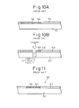
- FIG. 9A A sectional view of such a semiconductor device of the related art is shown in FIG. 9A.
- the semiconductor device 101 of the related art is mainly comprised of a silicon substrate 102 and does not have an interposer.
- One surface 102a of the silicon substrate 102 has formed on it an electronic element formation layer 103 including a transistor or other electronic element. This is electrically connected with a via hole electrode pad 110.
- An insulating film 104 prevents electrical connection of the via hole electrode pad 110 or main electrode pad 105 with the silicon substrate 102.
- the semiconductor element formation layer 103 and via hole electrode pad 110 have stacked over them an SiO 2 film 106 and an interconnection pattern 107.
- the SiO 2 film 106 has a via hole 106a opened in it.
- the interconnection pattern 107 and via hole electrode pad 110 are electrically connected through this opening.
- the via hole electrode pad 110 is provided integrally with the main electrode pad 105. Further, the main electrode pad 105 and the silicon substrate 102 under it have a through hole 111 opened in them.
- the through hole 111 is a characterizing feature of this type of semiconductor device and is provided to lead out the interconnection pattern 107 to the other surface 102b of the silicon substrate 102.
- the interconnection pattern 107 led out to the other surface 102b is provided with solder bumps 108 functioning as external connection terminals to be aligned in position with the terminals of the motherboard (not shown).
- FIG. 9C is a plan view of the semiconductor device 101 seen from the direction of the arrow A of FIG. 9A.
- the interconnection pattern 107 is omitted.
- the via hole 106a is a wide diameter circle at the bottom of which the via hole electrode pad 110 is exposed.
- the semiconductor device 101 is fabricated by building in a structure new to the existing semiconductor device (LSI etc.) 109 shown in section in FIG. 11. As will be explained using FIG. 11, the main electrode pad 105 is provided at the existing semiconductor device 109 as well. This is the location where originally bonding wires, stud bumps, etc. are bonded, signals are input and output, and power is supplied.
- the via hole electrode pad 110 (FIG. 9C) is one of the new structures and is not provided in existing semiconductor devices 109.
- the via hole electrode pad 110 is newly provided to increase the contact area with the interconnection pattern 107 (FIG. 9A) by providing a wide-diameter via hole 106a above it and to prevent peeling with the interconnection pattern 107 due to stress and poor electrical contact arising due to the same.
- a via hole pad 110 is newly provided as a part for electrical connection with the interconnection pattern 107 and, to ensure reliable electrical connection, a wide-diameter circular via hole 106a is opened above the via hole electrode pad 110.
- the through hole 111 is defined by an opening 102c of the silicon substrate 102, an opening 104a of the insulating film 104 and an opening 105a of the main electrode pad 105. Therefore, at the side walls of the through hole 111, the silicon substrate 102 and the main electrode pad 105 are insulated from each other by being distant from each other by a height D2 along the side walls.
- the height D2 is relatively small, so it is difficult to secure sufficient insulation between the silicon substrate 102 and the main electrode pad 105 at the side walls of the through hole 111.
- FIGS. 10A and 10B are sectional views of the semiconductor device 101 of the related art.
- a silicon substrate in the state shown in FIG. 10A is prepared.
- the insulating film 104, the main electrode pad 105 and the electronic element forming layer 103 are formed on the silicon substrate 102.
- a laser beam is fired from the side of the main electrode pad 105 and the portion struck by the laser beam vaporizes, whereby the through hole 111 is formed.
- the materials of the main electrode pad 105 and/or the silicon substrate 102 are vaporized by the laser beam and the vaporized conducting materials (silicon, aluminum, copper, etc.) deposit on the opening 104a of the insulating film 104, so there is the danger of electrically connecting the silicon substrate 102 and the main electrode pad 105.
- An object of the present invention is to provide a semiconductor device having a through hole passing through an electrode pad and a semiconductor substrate, in which sufficient insulation between the electrode pad and the semiconductor substrate at the side walls of the through hole is secured.
- Another object of the present invention is to provide a method of producing a semiconductor device including forming a through hole passing through an electrode pad and a semiconductor substrate, in which the danger of electrically connecting the electrode pad and the silicon substrate is reduced.
- a semiconductor device comprised of a semiconductor substrate; an electronic element formed on one surface of the semiconductor substrate; an electrode pad having an extension, formed on that one surface and electrically connected with the element; a through hole passing through the electrode pad and the semiconductor substrate; an insulating film formed on at least the other surface of the semiconductor substrate, an inner wall of the through hole, and the electrode pad including the extension; a via hole provided in the insulating film on the extension of the electrode pad; and an interconnection pattern electrically leading out the electrode pad to the other surface of the semiconductor substrate through the through hole and the via hole, said through hole having a diameter larger at a portion passing through the electrode pad than a portion passing through the semiconductor substrate.
- the interconnection pattern electrically leads out the electrode pad to the one surface of the semiconductor substrate as well. It is possible to stack a plurality of these semiconductor devices together and electrically connect interconnection patterns of facing surfaces of each bottom semiconductor device and top semiconductor device through external connection terminals.
- the through holes are filled by a conductor electrically connected with the interconnection patterns. It is possible to stack a plurality of these semiconductor devices and electrically connect conductors filled in corresponding through holes of each bottom semiconductor device and top semiconductor device through external connection terminals.
- a method of production of a semiconductor device comprising the steps of forming an electronic element on one surface of a semiconductor substrate; forming an electrode pad electrically connected with the element on the one surface of the semiconductor substrate; forming a first opening in the electrode pad by patterning; forming a second opening in the semiconductor substrate including the electronic element by firing through the first opening a laser beam of a smaller diameter than the diameter of the first opening, thereby defining a through hole by the first opening and the second opening; forming an insulating film on at least the other surface of the semiconductor substrate, an inner wall of the through hole, and the electrode pad including the extension; forming a via hole exposing part of the extension of the electrode pad by patterning the insulating film; forming a conductive film on the insulating film and in the via hole; and forming an interconnection pattern electrically leading the electrode pad to the other surface of the semiconductor substrate through the through hole and the via hole by patterning the conductive film.
- the step of forming the first opening and the step of forming the second opening include between them a step of polishing the other surface of the semiconductor substrate to reduce the thickness of the semiconductor substrate.
- the step of forming the via hole is performed by opening the insulating film by a laser beam.
- the interconnection pattern is formed so that the electrode pad is electrically led out to the one surface of the semiconductor substrate as well. It is possible to provide the steps of preparing a plurality of such semiconductor devices and stacking the semiconductor devices in a plurality of layers by electrically connecting the interconnection patterns of the semiconductor device through external connection terminals.
- the method includes a step of filling the through holes by a conductor electrically connected to the conductive film after the step of forming the conductive film. It is possible to provide the steps of preparing a plurality of such semiconductor devices and stacking the semiconductor devices in a plurality of layers by electrically connecting the conductors exposed from openings of corresponding through holes of the plurality of semiconductor devices through external connection terminals.
- a semiconductor device is provided with a semiconductor substrate and an electronic element formed on one surface of the semiconductor substrate.
- An electrode pad electrically connected with this element is formed on that surface of the semiconductor substrate.
- the electrode pad and the semiconductor substrate have a through hole passing through them.
- An insulating film is formed on the inner wall of that through hole. This insulating film is further formed on the other surface of the semiconductor substrate and on the electrode pad.
- the portion formed on the extension of the electrode pad is provided with a via hole.
- An interconnection pattern electrically leading the electrode pad to the other surface of the semiconductor substrate through the via hole and the through hole is provided in the semiconductor device.
- the diameter of the through hole is preferably made larger at the portion passing through the electrode pad (hereinafter called the "first opening”) than the portion passing through the semiconductor substrate (hereinafter called the "second opening").
- the interconnection pattern may electrically lead out the electrode pad to one surface of the semiconductor substrate.
- a method of production of a semiconductor device according to the present invention comprises the steps of:
- steps (c) and (d) among these steps since a laser beam of a smaller diameter than the diameter of the first opening is fired through the first opening after forming it, the laser beam can be prevented from contacting the first opening and vaporizing the material of the electrode pad, so the danger of the semiconductor substrate and the electrode pad ending up becoming electrically connected by vaporized material is lessened.
- this structure has the advantage that insulation between the electrode pad and semiconductor substrate at the side walls of the through hole is sufficiently secured.
- steps (c) and (d) may include between them a step of polishing the other surface of the semiconductor substrate to reduce the thickness of the semiconductor substrate.
- the semiconductor substrate is reduced in thickness before forming the second opening, it is possible to form the second opening by firing a laser beam for a short time and the heat damage to the semiconductor substrate arising due to the firing of the laser beam is reduced. Further, since the depth of working by the laser beam becomes shallow, the amount of vaporization of the material by the laser beam is reduced and the amount of the material vaporizing and depositing in the through hole is reduced. Due to this, it is possible to cleanly form the through hole.
- step (f) step of forming the via hole in the insulating film
- step (f) may be performed by opening the insulating film by a laser beam.
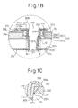
- FIGS. 1A, 1B, and 1C are sectional views of a semiconductor device according to a preferred embodiment of the present invention.
- FIG. 1B is an enlarged view of the area in the circle 1B of FIG. 1A
- FIG. 1C is an enlarged view of the area in the circle 1C of FIG. 1B.
- the semiconductor device 215 is provided with a silicon substrate 201 (semiconductor substrate).
- a silicon substrate 201 semiconductor substrate
- One surface 201a of this silicon substrate 201 is formed with a semiconductor element formation layer 202 in which a transistor or other electronic element is built.
- the semiconductor element formation layer 202 has an electrode pad 211 provided on it. While not shown, the electrode pad 211 is electrically connected with an element in the semiconductor element formation layer 202.
- the electrode pad 211 and silicon substrate 201 have the element formation layer 202 interposed between them.
- Reference numeral 204 indicates a passivation layer provided to protect the semiconductor element formation layer 202.
- the layer is for example comprised of SiO 2 .
- Reference numeral 212 indicates a through hole passing through the electrode pad 211 and silicon substrate 201.
- An SiO 2 film 209 (insulating film) is formed on its inner walls. The SiO 2 film 209 is also formed on the other surface 201b of the silicon substrate 201, on the electrode pad 211 and on the extension 211X of the electrode pad 211.
- the SiO 2 film 209 on the extension 211X of the electrode pad 211 is provided with a via hole 209a.
- the electrode pad 211 and an interconnection pattern 214 on the SiO 2 film are electrically connected through this via hole 209a.
- the through hole 212 is defined by the first opening 208 and the second opening 201c.
- the first opening 208 is the portion passing through the electrode pad 211
- the second opening 201c is the portion passing through the silicon substrate 201.
- the diameter R1 of the first opening 208 is made larger than the diameter R2 of the second opening 201c.
- R1 is about 50 to 70 ⁇ m, while R2 is made smaller than R1 or about 25 to 50 ⁇ m. What is important is that R1>R2.
- the present invention is not limited to the above numerical values.
- the second opening 201c is formed tapered, but as explained later, this is due to the formation of the second opening 201c by a laser beam.
- the shape is not limited to a tapered one.
- the advantages of the present invention can be obtained even if forming the second opening 201c straight in shape.
- the through hole 212 is hollow, but as shown in FIG. 7, it is also possible to fill the through hole 212 with a conductor 217 electrically connected with the interconnection pattern 214.
- the conductor 217 in this case, there is for example copper.
- interconnection pattern 214 is formed over the SiO 2 film 209 and extends to the other surface 201b of the silicon substrate 201 through the through hole 212.
- the interconnection pattern 214 functions to electrically connect the electrode pad 211 to the other surface 201b through the via hole 209a and through hole 212.
- solder bumps 210 functioning as external connection terminals.
- the external connection terminals are not limited to the solder bumps 210. Stud bumps or other known external connection terminals may also be used.
- the semiconductor device 215 is electrically and mechanically connected on the motherboard.
- the semiconductor device 215 may be used alone in this way or may be used stacked as explained above.
- FIG. 2 is a plan view of the semiconductor device 215 seen from the A side of FIG. 1A.
- the interconnection pattern 214 formed on the surface 201a is provided with a terminal part 214a.
- This terminal part 214a is provided to electrically lead out the electrode pad 211 to the surface 201a of the silicon substrate 201.
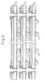
- FIG. 3 A sectional view of semiconductor devices 215 stacked in this way is shown in FIG. 3. As shown in FIG. 3, the interconnection patterns 214 of the facing surfaces of each top and bottom semiconductor device 215 are electrically connected through the solder bumps 210.
- This structure is a three-dimensional mounting structure obtained by stacking a plurality of the semiconductor devices. The planar size of each semiconductor device 215 is smaller than in the related art, so in this three-dimensional structure, it is possible to keep down the lateral spread as compared with the related art. This contributes to the higher density and smaller size of semiconductor packages as sought in recent years.
- the conductors 217a of the portions exposed from the openings 212a of the through holes 212 can be used instead of the terminal parts 214a, so the terminal parts 214a and the interconnection patterns 214 at the portions where solder bumps 210 are provided are unnecessary and the semiconductor devices 215 can be easily stacked.
- a sectional view of the semiconductor devices 215 in the case of stacking in this way is given in FIG. 8.
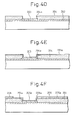
- FIGS. 4A to 4Q are sectional views of the semiconductor device in different steps of production.
- a silicon substrate 201 (semiconductor substrate) is prepared.
- This silicon substrate 201 is a substrate (wafer) for obtaining a large number of semiconductor devices.
- a transistor or other electronic element is formed on one surface 201a of the silicon substrate 201.
- reference numeral 202 shows a semiconductor element formation layer where the semiconductor element is formed.
- a film (not shown) comprised of aluminum (first metal) is formed on the semiconductor element formation layer 202 and this film patterned to form the bottom electrode pad 203.
- the thickness of the bottom electrode pad 203 is about 1 ⁇ m. Note that instead of aluminum, it is also possible to form the bottom electrode pad 203 by copper.
- the bottom electrode pad 203 and the silicon substrate 201 have the semiconductor element formation layer 202 interposed between them, the bottom electrode pad 203 is positioned above the silicon substrate 201 without contacting the silicon substrate 201. Further, while not particularly shown, the bottom electrode pad 203 is formed so as to be electrically connected with an interconnection layer in the semiconductor element formation layer 202.
- the bottom electrode pad 203 and the semiconductor element formation layer 202 have formed on them a passivation layer 204 comprised of SiO 2 etc.
- this passivation layer 204 is patterned to form an opening 204a where the bottom electrode pad 203 is exposed.
- the semiconductor substrate 201 formed with the bottom electrode pad 203 or semiconductor element formation layer 202 and the passivation layer 204 etc. is a general substrate usually produced by semiconductor manufacturers.
- the bottom electrode pad 203 is originally used as an electrode pad for wire bonding or bonding of external connection terminals (bumps etc.) (main electrode pad 110 in the example of the related art).
- a power feed layer 205a comprised of Cr (chrome) is formed on the passivation layer 204 and the exposed surface of the bottom electrode pad 203.
- the power feed layer 205a is formed by for example sputtering.
- a first photoresist 206 is coated on the power feed layer 205a.
- the first photoresist 206 is exposed and developed to form the first resist opening 206a superposed with the opening 204a of the passivation layer 204.
- the first photoresist 206 is removed, then the power feed layer 205a which had been formed under the first photoresist 206 is selectively etched to remove it.
- the top electrode pad 205 comprised of the power feed layer 205a and the electroplated copper layer 205b is completed.
- the thickness of the top electrode pad 205 is about 1 to 25 ⁇ m.
- the bottom electrode pad 203 and the top electrode pad 205 form the electrode pad 211.
- Part of the top electrode pad 205 extends leftwards in FIG. 4H to form an extension 211X of the electrode pad 211.
- a second photoresist 207 is formed on the passivation layer 204 and the exposed surface of the electrode pad 211. Further, the photoresist 207 is exposed and developed to form a second opening 207a exposing the electrode pad 211.
- the photoresist 207 is used as an etching mask to pattern the electrode pad 211 and form a first opening 208 in the electrode pad 211.
- the etching in this case is for example chemical etching or plasma etching.
- the diameter R1 of the first opening is about 50 to 70 ⁇ m, but should be suitably set in accordance with the diameter of the electrode pad 211.
- the other surface 201b of the silicon substrate 201 is polished to reduce the thickness of the silicon substrate 201 to about 50 to 150 ⁇ m.
- a laser beam having a smaller diameter than the diameter R1 of the first opening 208 is fired through the first opening 208.
- the laser there is a UV laser, YAG laser, or excimer laser.
- the portion struck by the laser beam vaporizes, whereby a second opening 201c is formed in the silicon substrate 201.
- the diameter R2 of this second opening 201c is about 25 to 50 ⁇ m.
- the through hole 212 is defined by the first opening 208 and the second opening 201c.
- the laser beam By firing a laser beam of a diameter smaller than the diameter R1 after forming the first opening 208, the laser beam is prevented from contacting the first opening 208 and vaporizing the material of the electrode pad 211 (aluminum or copper), so the danger of vaporized material depositing on the side walls of the through hole 212 and electrically connecting the silicon substrate 201 and electrode pad 211 is reduced.
- the material of the electrode pad 211 aluminum or copper
- this structure has the advantage that the insulation between the electrode pad 211 and the silicon substrate 201 at the side walls of the through hole 212 can be sufficiently secured.
- the silicon substrate 201 is reduced in thickness at the step of FIG. 4K before forming the second opening 201c, it is possible to form the second opening 201c by firing the laser beam for a short time, so heat damage to the silicon substrate 201 arising due to the laser beam can be reduced.
- the depth of working by the laser beam becomes shallow, the amount of the silicon vaporized by the laser beam is reduced and the amount of the silicon which is vaporized and deposits in the through hole 212 is reduced. Due to this, it is possible to cleanly form the through hole 212.
- step of FIG. 4K step of reducing the thickness of the silicon substrate 201 may be omitted.
- the second opening 201c illustrated is tapered, this is because a laser beam focused to a point by a focusing lens (not shown) instead of a laser beam of parallel light is used.
- the second opening 201c does not have to be tapered in shape.
- the advantages of the present invention can be obtained even if the second opening 201c is formed straight in shape.
- the second opening 201c may be formed by firing the laser beam from the other surface 201b of the silicon substrate 201 instead of firing the laser beam through the first opening 208. Even when doing this, it is similarly possible to prevent silicon vaporized by the laser from depositing on the electrode pad 211.
- the step shown in FIG. 6 may be performed between the steps of FIG. 4K and FIG. 4L.
- an SiO 2 film or other protective film 216 is formed by chemical vapor deposition (CVD) on the passivation layer 204, on the electrode pad 211 including the extension 211X, on the side walls of the first opening 208, and on the semiconductor element formation layer 202 exposed from the first opening 208.
- CVD chemical vapor deposition
- the protective film 216 is formed as explained above, it is possible to prevent damage to the electrode pad 211 or passivation layer 204 at the time of cleaning.
- an SiO 2 film 209 (insulating film) is formed at least on the other surface 201b of the semiconductor substrate 201, on the inner walls of the through hole 212, and on the electrode pad 211 including the extension 211X.
- the SiO 2 film 209 is formed by for example chemical vapor deposition (CVD).
- an SiO 2 film 209 may be formed on only the surface 201a of the semiconductor substrate 201 and the side walls of the through hole 212, then the SiO 2 film 209 formed on the other surface 201b.
- the SiO 2 film 209 is patterned to form the via hole 209a exposing part of the extension 211X of the electrode pad 211.
- the method of forming the via hole 209a for example, it is possible to form a resist (not shown) having an opening corresponding to that shape on the SiO 2 film 209 and selectively etch the SiO 2 film through that opening.
- the etching technique used at that time is for example chemical etching or plasma etching.
- a laser beam at the SiO 2 film 209 at the location where the via hole 209a should be formed to cause that portion to vaporize and thereby form the via hole 209a.
- a light-shielding mask (not shown) having a window of a shape corresponding to the via hole 209a against the laser beam and open the via hole 209a by the laser beam passing through that window.
- the step shown in FIG. 40 is performed.
- the conductive film 213 is formed on the SiO 2 film 209 and in the via hole 209a.
- the thickness of the conductive film 213 is about 1 to 20 ⁇ m.
- the conductive film 213, as shown in FIG. 4P, is comprised of a Cr (chrome) film 213a formed by sputtering, a copper film 213b formed over it also by sputtering, and an electroplated copper film 213c formed using the Cr (chrome) film 213a and copper film 213b as power feed layers.
- the structure of the conductive film 213, however, is not limited to this.
- Cr (chrome) film by sputtering, then form a Cu (copper), Ni (nickel), Au (gold), or other film by elecroless plating or electroplating on the Cr (chrome) film for use as the conductive film 213.
- the through hole 212 is hollow, but the present invention is not limited to this.
- the method of filling is not limited to the above method.
- the conductive film 213 does not become thick, so it is possible to finely pattern the conductive layer 213 in a later step. Note that whatever the method, the conductor 217 should electrically connect with the conductive film 213.
- the conductive film 213 is patterned to form interconnection patterns 214.
- the interconnection patterns 214 are formed on the two main surfaces 201a and 201b of the silicon substrate 201.
- the interconnection patterns 214 of the two main surfaces 201a and 201b are electrically connected through the through hole 212.
- solder bumps 210 serving as external connection terminals, then the substrate is diced, whereby semiconductor devices as shown in FIG. 1A are completed.
- the completed semiconductor devices 215 may be mounted alone on a motherboard (not shown) or may be stacked.
- terminal parts 214a are provided at the interconnection patterns 214.
- a plurality of the completed semiconductor devices 215 are prepared.
- the solder bumps 210 are made to reflow in the state with the solder bumps 210 abutting against the terminal parts 214a of the bottom semiconductor devices 215. After reflow, the temperature of the solder bumps 215 falls, whereby a semiconductor module of a three-dimensional mounting structure comprised of a large number of stacked semiconductor devices 215 is completed.
- the conductors 217a of the portions exposed from the openings 212a of the through holes 212 function as the above terminal parts 214a, so the terminal parts 214a and the interconnection patterns 214 of the locations of provision of the solder bumps 210 are unnecessary.
- the diameter of the through hole is made larger at the portion passing through the electrode pad than the portion passing through the semiconductor substrate so that insulation between the electrode pad and the semiconductor substrate can be sufficiently secured at the side walls of the through hole.
Applications Claiming Priority (2)
| Application Number | Priority Date | Filing Date | Title |
|---|---|---|---|
| JP2001180893A JP4053257B2 (ja) | 2001-06-14 | 2001-06-14 | 半導体装置の製造方法 |
| JP2001180893 | 2001-06-14 |
Publications (3)
| Publication Number | Publication Date |
|---|---|
| EP1267402A2 true EP1267402A2 (fr) | 2002-12-18 |
| EP1267402A3 EP1267402A3 (fr) | 2005-09-28 |
| EP1267402B1 EP1267402B1 (fr) | 2013-03-20 |
Family
ID=19021242
Family Applications (1)
| Application Number | Title | Priority Date | Filing Date |
|---|---|---|---|
| EP02291419A Expired - Fee Related EP1267402B1 (fr) | 2001-06-14 | 2002-06-07 | Dispositif semi-conducteur et méthode de fabrication associée |
Country Status (5)
| Country | Link |
|---|---|
| US (1) | US6703310B2 (fr) |
| EP (1) | EP1267402B1 (fr) |
| JP (1) | JP4053257B2 (fr) |
| CN (1) | CN100364092C (fr) |
| TW (1) | TW544904B (fr) |
Cited By (5)
| Publication number | Priority date | Publication date | Assignee | Title |
|---|---|---|---|---|
| EP1439576A2 (fr) | 2003-01-15 | 2004-07-21 | Shinko Electric Industries Co., Ltd. | Procédé de formation d'un trou traversant |
| EP1734576A1 (fr) * | 2005-06-17 | 2006-12-20 | Shinko Electric Industries Co., Ltd. | Composant semi-conducteur à trous métallisés et son procédé de fabrication |
| EP1768177A2 (fr) * | 2005-09-21 | 2007-03-28 | Shinko Electric Industries Co., Ltd. | Procédé pour la fabrication d'une puce semiconductrice |
| WO2007027880A3 (fr) * | 2005-09-01 | 2008-01-17 | Micron Technology Inc | Unites d'imagerie microelectroniques et leurs procedes de production au niveau tranche |
| EP3410470A1 (fr) * | 2005-04-08 | 2018-12-05 | Micron Technology, Inc. | Procédé et système de fabrication de composants semiconducteurs avec des interconnexions de fil traversant |
Families Citing this family (89)
| Publication number | Priority date | Publication date | Assignee | Title |
|---|---|---|---|---|
| JP2002373957A (ja) * | 2001-06-14 | 2002-12-26 | Shinko Electric Ind Co Ltd | 半導体装置及びその製造方法 |
| US7548430B1 (en) | 2002-05-01 | 2009-06-16 | Amkor Technology, Inc. | Buildup dielectric and metallization process and semiconductor package |
| US9691635B1 (en) | 2002-05-01 | 2017-06-27 | Amkor Technology, Inc. | Buildup dielectric layer having metallization pattern semiconductor package fabrication method |
| JP4280907B2 (ja) * | 2003-05-26 | 2009-06-17 | セイコーエプソン株式会社 | 半導体装置及びその製造方法 |
| JP2004349593A (ja) | 2003-05-26 | 2004-12-09 | Sanyo Electric Co Ltd | 半導体装置及びその製造方法 |
| US6934065B2 (en) * | 2003-09-18 | 2005-08-23 | Micron Technology, Inc. | Microelectronic devices and methods for packaging microelectronic devices |
| US8084866B2 (en) | 2003-12-10 | 2011-12-27 | Micron Technology, Inc. | Microelectronic devices and methods for filling vias in microelectronic devices |
| US7091124B2 (en) * | 2003-11-13 | 2006-08-15 | Micron Technology, Inc. | Methods for forming vias in microelectronic devices, and methods for packaging microelectronic devices |
| US7583862B2 (en) * | 2003-11-26 | 2009-09-01 | Aptina Imaging Corporation | Packaged microelectronic imagers and methods of packaging microelectronic imagers |
| JP4258367B2 (ja) * | 2003-12-18 | 2009-04-30 | 株式会社日立製作所 | 光部品搭載用パッケージ及びその製造方法 |
| US7211289B2 (en) * | 2003-12-18 | 2007-05-01 | Endicott Interconnect Technologies, Inc. | Method of making multilayered printed circuit board with filled conductive holes |
| US7253397B2 (en) * | 2004-02-23 | 2007-08-07 | Micron Technology, Inc. | Packaged microelectronic imagers and methods of packaging microelectronic imagers |
| US10811277B2 (en) | 2004-03-23 | 2020-10-20 | Amkor Technology, Inc. | Encapsulated semiconductor package |
| US11081370B2 (en) | 2004-03-23 | 2021-08-03 | Amkor Technology Singapore Holding Pte. Ltd. | Methods of manufacturing an encapsulated semiconductor device |
| US20050247894A1 (en) | 2004-05-05 | 2005-11-10 | Watkins Charles M | Systems and methods for forming apertures in microfeature workpieces |
| US7253957B2 (en) * | 2004-05-13 | 2007-08-07 | Micron Technology, Inc. | Integrated optics units and methods of manufacturing integrated optics units for use with microelectronic imagers |
| US8092734B2 (en) * | 2004-05-13 | 2012-01-10 | Aptina Imaging Corporation | Covers for microelectronic imagers and methods for wafer-level packaging of microelectronics imagers |
| US20050275750A1 (en) * | 2004-06-09 | 2005-12-15 | Salman Akram | Wafer-level packaged microelectronic imagers and processes for wafer-level packaging |
| US7498647B2 (en) * | 2004-06-10 | 2009-03-03 | Micron Technology, Inc. | Packaged microelectronic imagers and methods of packaging microelectronic imagers |
| US7262405B2 (en) * | 2004-06-14 | 2007-08-28 | Micron Technology, Inc. | Prefabricated housings for microelectronic imagers |
| US7199439B2 (en) | 2004-06-14 | 2007-04-03 | Micron Technology, Inc. | Microelectronic imagers and methods of packaging microelectronic imagers |
| US7294897B2 (en) * | 2004-06-29 | 2007-11-13 | Micron Technology, Inc. | Packaged microelectronic imagers and methods of packaging microelectronic imagers |
| US7232754B2 (en) * | 2004-06-29 | 2007-06-19 | Micron Technology, Inc. | Microelectronic devices and methods for forming interconnects in microelectronic devices |
| DE102004031878B3 (de) * | 2004-07-01 | 2005-10-06 | Epcos Ag | Elektrisches Mehrschichtbauelement mit zuverlässigem Lötkontakt |
| US7416913B2 (en) * | 2004-07-16 | 2008-08-26 | Micron Technology, Inc. | Methods of manufacturing microelectronic imaging units with discrete standoffs |
| US7189954B2 (en) * | 2004-07-19 | 2007-03-13 | Micron Technology, Inc. | Microelectronic imagers with optical devices and methods of manufacturing such microelectronic imagers |
| US7402453B2 (en) * | 2004-07-28 | 2008-07-22 | Micron Technology, Inc. | Microelectronic imaging units and methods of manufacturing microelectronic imaging units |
| US20060023107A1 (en) * | 2004-08-02 | 2006-02-02 | Bolken Todd O | Microelectronic imagers with optics supports having threadless interfaces and methods for manufacturing such microelectronic imagers |
| US7364934B2 (en) * | 2004-08-10 | 2008-04-29 | Micron Technology, Inc. | Microelectronic imaging units and methods of manufacturing microelectronic imaging units |
| US7397066B2 (en) * | 2004-08-19 | 2008-07-08 | Micron Technology, Inc. | Microelectronic imagers with curved image sensors and methods for manufacturing microelectronic imagers |
| US7223626B2 (en) * | 2004-08-19 | 2007-05-29 | Micron Technology, Inc. | Spacers for packaged microelectronic imagers and methods of making and using spacers for wafer-level packaging of imagers |
| US7429494B2 (en) | 2004-08-24 | 2008-09-30 | Micron Technology, Inc. | Microelectronic imagers with optical devices having integral reference features and methods for manufacturing such microelectronic imagers |
| US7115961B2 (en) * | 2004-08-24 | 2006-10-03 | Micron Technology, Inc. | Packaged microelectronic imaging devices and methods of packaging microelectronic imaging devices |
| US7425499B2 (en) * | 2004-08-24 | 2008-09-16 | Micron Technology, Inc. | Methods for forming interconnects in vias and microelectronic workpieces including such interconnects |
| US7276393B2 (en) * | 2004-08-26 | 2007-10-02 | Micron Technology, Inc. | Microelectronic imaging units and methods of manufacturing microelectronic imaging units |
| US20060043534A1 (en) * | 2004-08-26 | 2006-03-02 | Kirby Kyle K | Microfeature dies with porous regions, and associated methods and systems |
| SG120200A1 (en) * | 2004-08-27 | 2006-03-28 | Micron Technology Inc | Slanted vias for electrical circuits on circuit boards and other substrates |
| US7511262B2 (en) * | 2004-08-30 | 2009-03-31 | Micron Technology, Inc. | Optical device and assembly for use with imaging dies, and wafer-label imager assembly |
| US20070148807A1 (en) * | 2005-08-22 | 2007-06-28 | Salman Akram | Microelectronic imagers with integrated optical devices and methods for manufacturing such microelectronic imagers |
| US7646075B2 (en) * | 2004-08-31 | 2010-01-12 | Micron Technology, Inc. | Microelectronic imagers having front side contacts |
| US7300857B2 (en) * | 2004-09-02 | 2007-11-27 | Micron Technology, Inc. | Through-wafer interconnects for photoimager and memory wafers |
| US7279407B2 (en) | 2004-09-02 | 2007-10-09 | Micron Technology, Inc. | Selective nickel plating of aluminum, copper, and tungsten structures |
| US7271482B2 (en) * | 2004-12-30 | 2007-09-18 | Micron Technology, Inc. | Methods for forming interconnects in microelectronic workpieces and microelectronic workpieces formed using such methods |
| US7214919B2 (en) * | 2005-02-08 | 2007-05-08 | Micron Technology, Inc. | Microelectronic imaging units and methods of manufacturing microelectronic imaging units |
| US7303931B2 (en) * | 2005-02-10 | 2007-12-04 | Micron Technology, Inc. | Microfeature workpieces having microlenses and methods of forming microlenses on microfeature workpieces |
| US20060177999A1 (en) * | 2005-02-10 | 2006-08-10 | Micron Technology, Inc. | Microelectronic workpieces and methods for forming interconnects in microelectronic workpieces |
| US8278738B2 (en) * | 2005-02-17 | 2012-10-02 | Sharp Kabushiki Kaisha | Method of producing semiconductor device and semiconductor device |
| US7190039B2 (en) * | 2005-02-18 | 2007-03-13 | Micron Technology, Inc. | Microelectronic imagers with shaped image sensors and methods for manufacturing microelectronic imagers |
| US7485967B2 (en) * | 2005-03-10 | 2009-02-03 | Sanyo Electric Co., Ltd. | Semiconductor device with via hole for electric connection |
| DE102005042072A1 (de) * | 2005-06-01 | 2006-12-14 | Forschungsverbund Berlin E.V. | Verfahren zur Erzeugung von vertikalen elektrischen Kontaktverbindungen in Halbleiterwafern |
| US7795134B2 (en) * | 2005-06-28 | 2010-09-14 | Micron Technology, Inc. | Conductive interconnect structures and formation methods using supercritical fluids |
| US20060290001A1 (en) * | 2005-06-28 | 2006-12-28 | Micron Technology, Inc. | Interconnect vias and associated methods of formation |
| JP4758712B2 (ja) | 2005-08-29 | 2011-08-31 | 新光電気工業株式会社 | 半導体装置の製造方法 |
| JP4828182B2 (ja) * | 2005-08-31 | 2011-11-30 | 新光電気工業株式会社 | 半導体装置の製造方法 |
| DE102005042074A1 (de) * | 2005-08-31 | 2007-03-08 | Forschungsverbund Berlin E.V. | Verfahren zur Erzeugung von Durchkontaktierungen in Halbleiterwafern |
| US7288757B2 (en) * | 2005-09-01 | 2007-10-30 | Micron Technology, Inc. | Microelectronic imaging devices and associated methods for attaching transmissive elements |
| US7772115B2 (en) * | 2005-09-01 | 2010-08-10 | Micron Technology, Inc. | Methods for forming through-wafer interconnects, intermediate structures so formed, and devices and systems having at least one solder dam structure |
| US7863187B2 (en) | 2005-09-01 | 2011-01-04 | Micron Technology, Inc. | Microfeature workpieces and methods for forming interconnects in microfeature workpieces |
| US7262134B2 (en) | 2005-09-01 | 2007-08-28 | Micron Technology, Inc. | Microfeature workpieces and methods for forming interconnects in microfeature workpieces |
| US7622377B2 (en) * | 2005-09-01 | 2009-11-24 | Micron Technology, Inc. | Microfeature workpiece substrates having through-substrate vias, and associated methods of formation |
| JP5222459B2 (ja) | 2005-10-18 | 2013-06-26 | 新光電気工業株式会社 | 半導体チップの製造方法、マルチチップパッケージ |
| US7749899B2 (en) | 2006-06-01 | 2010-07-06 | Micron Technology, Inc. | Microelectronic workpieces and methods and systems for forming interconnects in microelectronic workpieces |
| US7629249B2 (en) * | 2006-08-28 | 2009-12-08 | Micron Technology, Inc. | Microfeature workpieces having conductive interconnect structures formed by chemically reactive processes, and associated systems and methods |
| US8021981B2 (en) | 2006-08-30 | 2011-09-20 | Micron Technology, Inc. | Redistribution layers for microfeature workpieces, and associated systems and methods |
| US7902643B2 (en) | 2006-08-31 | 2011-03-08 | Micron Technology, Inc. | Microfeature workpieces having interconnects and conductive backplanes, and associated systems and methods |
| US7812461B2 (en) | 2007-03-27 | 2010-10-12 | Micron Technology, Inc. | Method and apparatus providing integrated circuit having redistribution layer with recessed connectors |
| JP2008305938A (ja) * | 2007-06-07 | 2008-12-18 | Toshiba Corp | 半導体装置および半導体装置の製造方法 |
| JP2009055004A (ja) * | 2007-08-24 | 2009-03-12 | Honda Motor Co Ltd | 貫通配線構造 |
| SG150410A1 (en) | 2007-08-31 | 2009-03-30 | Micron Technology Inc | Partitioned through-layer via and associated systems and methods |
| US7884015B2 (en) | 2007-12-06 | 2011-02-08 | Micron Technology, Inc. | Methods for forming interconnects in microelectronic workpieces and microelectronic workpieces formed using such methods |
| US8084854B2 (en) * | 2007-12-28 | 2011-12-27 | Micron Technology, Inc. | Pass-through 3D interconnect for microelectronic dies and associated systems and methods |
| US8138577B2 (en) * | 2008-03-27 | 2012-03-20 | Hong Kong Applied Science And Technology Research Institute Co., Ltd. | Pulse-laser bonding method for through-silicon-via based stacking of electronic components |
| US7741156B2 (en) * | 2008-05-27 | 2010-06-22 | Stats Chippac, Ltd. | Semiconductor device and method of forming through vias with reflowed conductive material |
| JP2010040862A (ja) * | 2008-08-06 | 2010-02-18 | Fujikura Ltd | 半導体装置 |
| US7872332B2 (en) | 2008-09-11 | 2011-01-18 | Micron Technology, Inc. | Interconnect structures for stacked dies, including penetrating structures for through-silicon vias, and associated systems and methods |
| US8030780B2 (en) * | 2008-10-16 | 2011-10-04 | Micron Technology, Inc. | Semiconductor substrates with unitary vias and via terminals, and associated systems and methods |
| JP5308145B2 (ja) | 2008-12-19 | 2013-10-09 | ルネサスエレクトロニクス株式会社 | 半導体装置 |
| JP5471268B2 (ja) * | 2008-12-26 | 2014-04-16 | 大日本印刷株式会社 | 貫通電極基板及びその製造方法 |
| US20100194465A1 (en) * | 2009-02-02 | 2010-08-05 | Ali Salih | Temperature compensated current source and method therefor |
| JP5330863B2 (ja) * | 2009-03-04 | 2013-10-30 | パナソニック株式会社 | 半導体装置の製造方法 |
| KR20100110613A (ko) * | 2009-04-03 | 2010-10-13 | 삼성전자주식회사 | 반도체 장치 및 그 제조방법 |
| JP5574639B2 (ja) * | 2009-08-21 | 2014-08-20 | 三菱電機株式会社 | 半導体装置およびその製造方法 |
| KR101078740B1 (ko) * | 2009-12-31 | 2011-11-02 | 주식회사 하이닉스반도체 | 스택 패키지 및 그의 제조방법 |
| TWI455271B (zh) * | 2011-05-24 | 2014-10-01 | 矽品精密工業股份有限公司 | 半導體元件結構及其製法 |
| US8796822B2 (en) | 2011-10-07 | 2014-08-05 | Freescale Semiconductor, Inc. | Stacked semiconductor devices |
| US9076664B2 (en) * | 2011-10-07 | 2015-07-07 | Freescale Semiconductor, Inc. | Stacked semiconductor die with continuous conductive vias |
| EP2838114A3 (fr) * | 2013-08-12 | 2015-04-08 | Xintec Inc. | Emballage de puces |
| US9082757B2 (en) | 2013-10-31 | 2015-07-14 | Freescale Semiconductor, Inc. | Stacked semiconductor devices |
| US10002653B2 (en) | 2014-10-28 | 2018-06-19 | Nxp Usa, Inc. | Die stack address bus having a programmable width |
Citations (2)
| Publication number | Priority date | Publication date | Assignee | Title |
|---|---|---|---|---|
| WO1996013062A1 (fr) * | 1994-10-19 | 1996-05-02 | Ceram Incorporated | Dispositif et procede de fabrication d'empilements de series de plaquettes |
| EP1077494A2 (fr) * | 1999-08-19 | 2001-02-21 | Sharp Kabushiki Kaisha | Transistor bipolaire à hétérojonction et procédé pour sa fabrication |
Family Cites Families (10)
| Publication number | Priority date | Publication date | Assignee | Title |
|---|---|---|---|---|
| JPS5710251A (en) * | 1980-06-20 | 1982-01-19 | Toshiba Corp | Semiconductor device |
| JPS59110141A (ja) * | 1982-12-15 | 1984-06-26 | Fuji Electric Co Ltd | 半導体装置の製造方法 |
| US5065228A (en) * | 1989-04-04 | 1991-11-12 | Olin Corporation | G-TAB having particular through hole |
| US5527741A (en) * | 1994-10-11 | 1996-06-18 | Martin Marietta Corporation | Fabrication and structures of circuit modules with flexible interconnect layers |
| US5874770A (en) * | 1996-10-10 | 1999-02-23 | General Electric Company | Flexible interconnect film including resistor and capacitor layers |
| US6054761A (en) * | 1998-12-01 | 2000-04-25 | Fujitsu Limited | Multi-layer circuit substrates and electrical assemblies having conductive composition connectors |
| RU2134466C1 (ru) * | 1998-12-08 | 1999-08-10 | Таран Александр Иванович | Носитель кристалла ис |
| US6039889A (en) * | 1999-01-12 | 2000-03-21 | Fujitsu Limited | Process flows for formation of fine structure layer pairs on flexible films |
| JP2000246475A (ja) * | 1999-02-25 | 2000-09-12 | Seiko Epson Corp | レーザ光による加工方法 |
| IL133453A0 (en) * | 1999-12-10 | 2001-04-30 | Shellcase Ltd | Methods for producing packaged integrated circuit devices and packaged integrated circuit devices produced thereby |
-
2001
- 2001-06-14 JP JP2001180893A patent/JP4053257B2/ja not_active Expired - Fee Related
-
2002
- 2002-06-06 US US10/162,598 patent/US6703310B2/en not_active Expired - Lifetime
- 2002-06-07 EP EP02291419A patent/EP1267402B1/fr not_active Expired - Fee Related
- 2002-06-13 TW TW091112926A patent/TW544904B/zh not_active IP Right Cessation
- 2002-06-14 CN CNB021213445A patent/CN100364092C/zh not_active Expired - Fee Related
Patent Citations (2)
| Publication number | Priority date | Publication date | Assignee | Title |
|---|---|---|---|---|
| WO1996013062A1 (fr) * | 1994-10-19 | 1996-05-02 | Ceram Incorporated | Dispositif et procede de fabrication d'empilements de series de plaquettes |
| EP1077494A2 (fr) * | 1999-08-19 | 2001-02-21 | Sharp Kabushiki Kaisha | Transistor bipolaire à hétérojonction et procédé pour sa fabrication |
Cited By (9)
| Publication number | Priority date | Publication date | Assignee | Title |
|---|---|---|---|---|
| EP1439576A2 (fr) | 2003-01-15 | 2004-07-21 | Shinko Electric Industries Co., Ltd. | Procédé de formation d'un trou traversant |
| EP1439576A3 (fr) * | 2003-01-15 | 2007-04-25 | Shinko Electric Industries Co., Ltd. | Procédé de formation d'un trou traversant |
| EP3410470A1 (fr) * | 2005-04-08 | 2018-12-05 | Micron Technology, Inc. | Procédé et système de fabrication de composants semiconducteurs avec des interconnexions de fil traversant |
| EP1734576A1 (fr) * | 2005-06-17 | 2006-12-20 | Shinko Electric Industries Co., Ltd. | Composant semi-conducteur à trous métallisés et son procédé de fabrication |
| US7524753B2 (en) | 2005-06-17 | 2009-04-28 | Shinko Electric Industries Co., Ltd. | Semiconductor device having through electrode and method of manufacturing the same |
| WO2007027880A3 (fr) * | 2005-09-01 | 2008-01-17 | Micron Technology Inc | Unites d'imagerie microelectroniques et leurs procedes de production au niveau tranche |
| US7452743B2 (en) | 2005-09-01 | 2008-11-18 | Aptina Imaging Corporation | Microelectronic imaging units and methods of manufacturing microelectronic imaging units at the wafer level |
| EP1768177A2 (fr) * | 2005-09-21 | 2007-03-28 | Shinko Electric Industries Co., Ltd. | Procédé pour la fabrication d'une puce semiconductrice |
| EP1768177A3 (fr) * | 2005-09-21 | 2011-06-22 | Shinko Electric Industries Co., Ltd. | Procédé pour la fabrication d'une puce semiconductrice |
Also Published As
| Publication number | Publication date |
|---|---|
| JP4053257B2 (ja) | 2008-02-27 |
| EP1267402A3 (fr) | 2005-09-28 |
| CN1392611A (zh) | 2003-01-22 |
| JP2002373895A (ja) | 2002-12-26 |
| CN100364092C (zh) | 2008-01-23 |
| EP1267402B1 (fr) | 2013-03-20 |
| US6703310B2 (en) | 2004-03-09 |
| TW544904B (en) | 2003-08-01 |
| US20020190371A1 (en) | 2002-12-19 |
Similar Documents
| Publication | Publication Date | Title |
|---|---|---|
| EP1267402B1 (fr) | Dispositif semi-conducteur et méthode de fabrication associée | |
| US6699787B2 (en) | Semiconductor device and method of production of same | |
| JP5222459B2 (ja) | 半導体チップの製造方法、マルチチップパッケージ | |
| US6642615B2 (en) | Semiconductor device and method of manufacturing the same, circuit board and electronic instrument | |
| KR900006511B1 (ko) | 반도체장치를 제조하는 방법 | |
| KR100641696B1 (ko) | 반도체 장치 제조방법 | |
| US7256490B2 (en) | Test carrier for semiconductor components having conductors defined by grooves | |
| KR19990035858A (ko) | 전기 회로상에 영구 결속을 위한 돌출 금속 접촉부 형성 방법 | |
| JP2002513510A (ja) | 電子デバイス用インターフェース構造 | |
| KR20040101924A (ko) | 반도체 장치 및 그 제조 방법 | |
| KR20010018694A (ko) | 3차원 적층 칩 패키지 제조 방법 | |
| US20080142945A1 (en) | Semiconductor package with redistribution layer of semiconductor chip directly contacted with substrate and method of fabricating the same | |
| US7704792B2 (en) | Semiconductor device and method of manufacturing the same | |
| US20050026416A1 (en) | Encapsulated pin structure for improved reliability of wafer | |
| JPH11204678A (ja) | 半導体装置及びその製造方法 | |
| US7193297B2 (en) | Semiconductor device, method for manufacturing the same, circuit substrate and electronic device | |
| US20070102807A1 (en) | Coupling substrate for semiconductor components and method for producing the same | |
| US6646357B2 (en) | Semiconductor device and method of production of same | |
| US11272614B2 (en) | Printed wiring board and method for manufacturing the same | |
| KR20000070491A (ko) | 반도체 웨이퍼상에 일정 구조의 금속을 형성하는 방법 | |
| CN112820711A (zh) | 集成基板结构、重布线结构及其制造方法 | |
| CN113223971A (zh) | 半导体器件及制造该半导体器件的方法 | |
| JP2001053189A (ja) | 配線基板とその製造方法 | |
| KR20010062919A (ko) | 웨이퍼 레벨 패키지 및 그의 제조 방법 |
Legal Events
| Date | Code | Title | Description |
|---|---|---|---|
| PUAI | Public reference made under article 153(3) epc to a published international application that has entered the european phase |
Free format text: ORIGINAL CODE: 0009012 |
|
| AK | Designated contracting states |
Kind code of ref document: A2 Designated state(s): AT BE CH CY DE DK ES FI FR GB GR IE IT LI LU MC NL PT SE TR |
|
| AX | Request for extension of the european patent |
Free format text: AL;LT;LV;MK;RO;SI |
|
| PUAL | Search report despatched |
Free format text: ORIGINAL CODE: 0009013 |
|
| AK | Designated contracting states |
Kind code of ref document: A3 Designated state(s): AT BE CH CY DE DK ES FI FR GB GR IE IT LI LU MC NL PT SE TR |
|
| AX | Request for extension of the european patent |
Extension state: AL LT LV MK RO SI |
|
| 17P | Request for examination filed |
Effective date: 20051012 |
|
| AKX | Designation fees paid |
Designated state(s): FR |
|
| REG | Reference to a national code |
Ref country code: DE Ref legal event code: 8566 |
|
| 17Q | First examination report despatched |
Effective date: 20080814 |
|
| RIC1 | Information provided on ipc code assigned before grant |
Ipc: H01L 25/065 20060101ALI20120814BHEP Ipc: H01L 21/768 20060101ALI20120814BHEP Ipc: H01L 21/98 20060101ALI20120814BHEP Ipc: H01L 23/48 20060101AFI20120814BHEP |
|
| GRAP | Despatch of communication of intention to grant a patent |
Free format text: ORIGINAL CODE: EPIDOSNIGR1 |
|
| GRAS | Grant fee paid |
Free format text: ORIGINAL CODE: EPIDOSNIGR3 |
|
| GRAA | (expected) grant |
Free format text: ORIGINAL CODE: 0009210 |
|
| AK | Designated contracting states |
Kind code of ref document: B1 Designated state(s): FR |
|
| PLBE | No opposition filed within time limit |
Free format text: ORIGINAL CODE: 0009261 |
|
| STAA | Information on the status of an ep patent application or granted ep patent |
Free format text: STATUS: NO OPPOSITION FILED WITHIN TIME LIMIT |
|
| 26N | No opposition filed |
Effective date: 20140102 |
|
| REG | Reference to a national code |
Ref country code: FR Ref legal event code: PLFP Year of fee payment: 15 |
|
| PGFP | Annual fee paid to national office [announced via postgrant information from national office to epo] |
Ref country code: FR Payment date: 20160516 Year of fee payment: 15 |
|
| REG | Reference to a national code |
Ref country code: FR Ref legal event code: ST Effective date: 20180228 |
|
| PG25 | Lapsed in a contracting state [announced via postgrant information from national office to epo] |
Ref country code: FR Free format text: LAPSE BECAUSE OF NON-PAYMENT OF DUE FEES Effective date: 20170630 |