EP1267381A1 - Method for low temeperature sharpening of silicon based field emitter tips - Google Patents
Method for low temeperature sharpening of silicon based field emitter tips Download PDFInfo
- Publication number
- EP1267381A1 EP1267381A1 EP02253772A EP02253772A EP1267381A1 EP 1267381 A1 EP1267381 A1 EP 1267381A1 EP 02253772 A EP02253772 A EP 02253772A EP 02253772 A EP02253772 A EP 02253772A EP 1267381 A1 EP1267381 A1 EP 1267381A1
- Authority
- EP
- European Patent Office
- Prior art keywords
- silicon
- field emitter
- emitter tip
- well
- based field
- Prior art date
- Legal status (The legal status is an assumption and is not a legal conclusion. Google has not performed a legal analysis and makes no representation as to the accuracy of the status listed.)
- Withdrawn
Links
- XUIMIQQOPSSXEZ-UHFFFAOYSA-N Silicon Chemical compound [Si] XUIMIQQOPSSXEZ-UHFFFAOYSA-N 0.000 title claims abstract description 95
- 229910052710 silicon Inorganic materials 0.000 title claims abstract description 95
- 239000010703 silicon Substances 0.000 title claims abstract description 95
- 238000000034 method Methods 0.000 title claims abstract description 40
- 238000005530 etching Methods 0.000 claims abstract description 18
- BLIQUJLAJXRXSG-UHFFFAOYSA-N 1-benzyl-3-(trifluoromethyl)pyrrolidin-1-ium-3-carboxylate Chemical compound C1C(C(=O)O)(C(F)(F)F)CCN1CC1=CC=CC=C1 BLIQUJLAJXRXSG-UHFFFAOYSA-N 0.000 claims abstract description 6
- 229920002120 photoresistant polymer Polymers 0.000 claims description 18
- 239000002184 metal Substances 0.000 claims description 13
- 239000000203 mixture Substances 0.000 claims description 5
- 229910015844 BCl3 Inorganic materials 0.000 claims description 4
- QAOWNCQODCNURD-UHFFFAOYSA-N Sulfuric acid Chemical compound OS(O)(=O)=O QAOWNCQODCNURD-UHFFFAOYSA-N 0.000 claims description 4
- 239000002904 solvent Substances 0.000 claims description 4
- FAQYAMRNWDIXMY-UHFFFAOYSA-N trichloroborane Chemical compound ClB(Cl)Cl FAQYAMRNWDIXMY-UHFFFAOYSA-N 0.000 claims description 4
- LSNNMFCWUKXFEE-UHFFFAOYSA-M Bisulfite Chemical compound OS([O-])=O LSNNMFCWUKXFEE-UHFFFAOYSA-M 0.000 claims description 2
- 229910003910 SiCl4 Inorganic materials 0.000 claims description 2
- RJCQBQGAPKAMLL-UHFFFAOYSA-N bromotrifluoromethane Chemical compound FC(F)(F)Br RJCQBQGAPKAMLL-UHFFFAOYSA-N 0.000 claims description 2
- 150000008280 chlorinated hydrocarbons Chemical class 0.000 claims description 2
- FDNAPBUWERUEDA-UHFFFAOYSA-N silicon tetrachloride Chemical compound Cl[Si](Cl)(Cl)Cl FDNAPBUWERUEDA-UHFFFAOYSA-N 0.000 claims description 2
- KRVSOGSZCMJSLX-UHFFFAOYSA-L chromic acid Substances O[Cr](O)(=O)=O KRVSOGSZCMJSLX-UHFFFAOYSA-L 0.000 claims 1
- AWJWCTOOIBYHON-UHFFFAOYSA-N furo[3,4-b]pyrazine-5,7-dione Chemical compound C1=CN=C2C(=O)OC(=O)C2=N1 AWJWCTOOIBYHON-UHFFFAOYSA-N 0.000 claims 1
- 238000000059 patterning Methods 0.000 claims 1
- 239000010410 layer Substances 0.000 description 15
- 238000003860 storage Methods 0.000 description 12
- IGELFKKMDLGCJO-UHFFFAOYSA-N xenon difluoride Chemical compound F[Xe]F IGELFKKMDLGCJO-UHFFFAOYSA-N 0.000 description 10
- 238000003491 array Methods 0.000 description 8
- 238000004519 manufacturing process Methods 0.000 description 8
- 239000000463 material Substances 0.000 description 8
- 239000000758 substrate Substances 0.000 description 8
- VYPSYNLAJGMNEJ-UHFFFAOYSA-N Silicium dioxide Chemical compound O=[Si]=O VYPSYNLAJGMNEJ-UHFFFAOYSA-N 0.000 description 6
- 230000005684 electric field Effects 0.000 description 6
- 239000007789 gas Substances 0.000 description 6
- 238000010894 electron beam technology Methods 0.000 description 5
- 230000004888 barrier function Effects 0.000 description 3
- 229910052681 coesite Inorganic materials 0.000 description 3
- 229910052906 cristobalite Inorganic materials 0.000 description 3
- 230000007812 deficiency Effects 0.000 description 3
- 238000012986 modification Methods 0.000 description 3
- 230000004048 modification Effects 0.000 description 3
- 238000001020 plasma etching Methods 0.000 description 3
- 238000005381 potential energy Methods 0.000 description 3
- 239000004065 semiconductor Substances 0.000 description 3
- 239000000377 silicon dioxide Substances 0.000 description 3
- 229910052682 stishovite Inorganic materials 0.000 description 3
- 239000002344 surface layer Substances 0.000 description 3
- 229910052905 tridymite Inorganic materials 0.000 description 3
- KRHYYFGTRYWZRS-UHFFFAOYSA-N Fluorane Chemical compound F KRHYYFGTRYWZRS-UHFFFAOYSA-N 0.000 description 2
- 238000013500 data storage Methods 0.000 description 2
- 230000003647 oxidation Effects 0.000 description 2
- 238000007254 oxidation reaction Methods 0.000 description 2
- 235000012431 wafers Nutrition 0.000 description 2
- 238000001039 wet etching Methods 0.000 description 2
- KZBUYRJDOAKODT-UHFFFAOYSA-N Chlorine Chemical compound ClCl KZBUYRJDOAKODT-UHFFFAOYSA-N 0.000 description 1
- YCKRFDGAMUMZLT-UHFFFAOYSA-N Fluorine atom Chemical compound [F] YCKRFDGAMUMZLT-UHFFFAOYSA-N 0.000 description 1
- OAICVXFJPJFONN-UHFFFAOYSA-N Phosphorus Chemical compound [P] OAICVXFJPJFONN-UHFFFAOYSA-N 0.000 description 1
- 230000002411 adverse Effects 0.000 description 1
- 229910021417 amorphous silicon Inorganic materials 0.000 description 1
- 238000006243 chemical reaction Methods 0.000 description 1
- 239000011248 coating agent Substances 0.000 description 1
- 238000000576 coating method Methods 0.000 description 1
- 230000000295 complement effect Effects 0.000 description 1
- 239000004020 conductor Substances 0.000 description 1
- 239000013078 crystal Substances 0.000 description 1
- 230000003247 decreasing effect Effects 0.000 description 1
- 230000001419 dependent effect Effects 0.000 description 1
- 238000000605 extraction Methods 0.000 description 1
- 229910052731 fluorine Inorganic materials 0.000 description 1
- 239000011737 fluorine Substances 0.000 description 1
- 230000003116 impacting effect Effects 0.000 description 1
- 230000008018 melting Effects 0.000 description 1
- 238000002844 melting Methods 0.000 description 1
- 229910044991 metal oxide Inorganic materials 0.000 description 1
- 150000004706 metal oxides Chemical class 0.000 description 1
- 229910021420 polycrystalline silicon Inorganic materials 0.000 description 1
- 238000010791 quenching Methods 0.000 description 1
- 230000000171 quenching effect Effects 0.000 description 1
- ABTOQLMXBSRXSM-UHFFFAOYSA-N silicon tetrafluoride Chemical class F[Si](F)(F)F ABTOQLMXBSRXSM-UHFFFAOYSA-N 0.000 description 1
- 239000007787 solid Substances 0.000 description 1
- 239000000126 substance Substances 0.000 description 1
- 230000005641 tunneling Effects 0.000 description 1
- 230000008016 vaporization Effects 0.000 description 1
Images


Classifications
-
- H—ELECTRICITY
- H01—ELECTRIC ELEMENTS
- H01J—ELECTRIC DISCHARGE TUBES OR DISCHARGE LAMPS
- H01J9/00—Apparatus or processes specially adapted for the manufacture, installation, removal, maintenance of electric discharge tubes, discharge lamps, or parts thereof; Recovery of material from discharge tubes or lamps
- H01J9/02—Manufacture of electrodes or electrode systems
- H01J9/022—Manufacture of electrodes or electrode systems of cold cathodes
- H01J9/025—Manufacture of electrodes or electrode systems of cold cathodes of field emission cathodes
Definitions
- the present invention relates to silicon-based field emitter tips and, in particular, to a method for sharpening silicon-based field emitter tips at low temperatures.
- the present invention relates to design and manufacture of field emitter tips, including silicon-based field emitter tips.
- field emitter tips including silicon-based field emitter tips.
- a brief discussion of field emission and the principles of design and operation of field emitter tips is therefore first provided in the following paragraphs, with reference to Figures1 .
- Figure 1 illustrates principles of design and operation of a silicon-based field emitter tip.
- the field emitter tip 102 rises to a very sharp point 104 from a silicon-substrate cathode 106, or electron source.
- a localized electric field is applied in the vicinity of the tip by a first anode 108, or electron sink, having a disk-shaped aperture 110 above and around the point 104 of the field emitter tip 102.
- a second cathode layer 112 is located above the first anode 108, also with a disk-shaped aperture 114 aligned directly above the disk-shaped aperture 110 of the first anode layer 108.
- This second cathode layer 112 acts as a lens, applying a repulsive electronic field to focus the emitted electrons into a narrow beam.
- the emitted electrons are accelerated towards a target anode 118, impacting in a small region 120 of the target anode defined by the direction and width of the emitted electron beam 116.
- Figure 1 illustrates a single field emitter tip, silicon-based field emitter tips are commonly micro-manufactured by microchip fabrication techniques as regular arrays, or grids, of field emitter tips.
- Silicon-based field emitter tips are commonly located on the surface of complementary metal-oxide semiconductor ("CMOS") wafers.
- CMOS complementary metal-oxide semiconductor
- the current density of emitted electrons from a field emitter tips greatly increases with a decrease in the radius of the tip. Therefore, since it is desirable to achieve high current densities from silicon-based field emitter tips, tip sharpening procedures are normally employed in the final stage or stages of silicon-based field emitter tip array manufacture.
- Figures 2A-C illustrate a currently-available tip-sharpening procedure.
- a blunt silicon-based field emitter tip 202 rises from a flat silicon substrate 204.
- FIG. 2B shows the field emitter tip shown in Figure 2A following thermal oxidation.
- the thin SIO 2 layer 206 is grown inward from the surface of the field emitter tip and silicon substrate to produce a sharp, silicon-based field emitter tip 208 embedded within the thin SiO 2 coating 206.
- the thin SIO 2 layer is removed by hydrofluoric acid, HF, wet etching.
- Figure 2C shows the final sharp field emitter tip following HF wet etching.
- the point 2 10 of the final sharp field emitter tip may have a breadth of between 10 and several hundred Angstroms.
- Thermal-oxide-based tip sharpening is effective and is commonly employed in current silicon-based field emitter tip application methodologies. However, especially when used to sharpen silicon-based field emitter tips fabricated on the surface of CMOS wafers, the thermal oxidation tip sharpening process has clear deficiencies due to the relatively high temperatures, commonly greater than 900 C, necessary to grow the surface layer of SiO 2 .
- a first deficiency is that the underlying CMOS circuitry may employ low-melting-point conductors that can be degraded by high temperature exposure. Thus, extremely precise application of heat must be carried out to grow the surface layer of SIO 2 while not adversely effecting underlying CMOS circuitry.
- One embodiment of the present invention provides an efficient and economical process for sharpening silicon-based field emitter tips at low temperatures.
- a rough field emitter tip is carved out from a silicon well below a photoresist mask by isotropic plasma etching.
- the photoresist mask is removed, and the rough silicon-based field emitter tip that results is sharpened by isotropic xenon difluoride, XeF 2 etching.
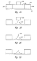
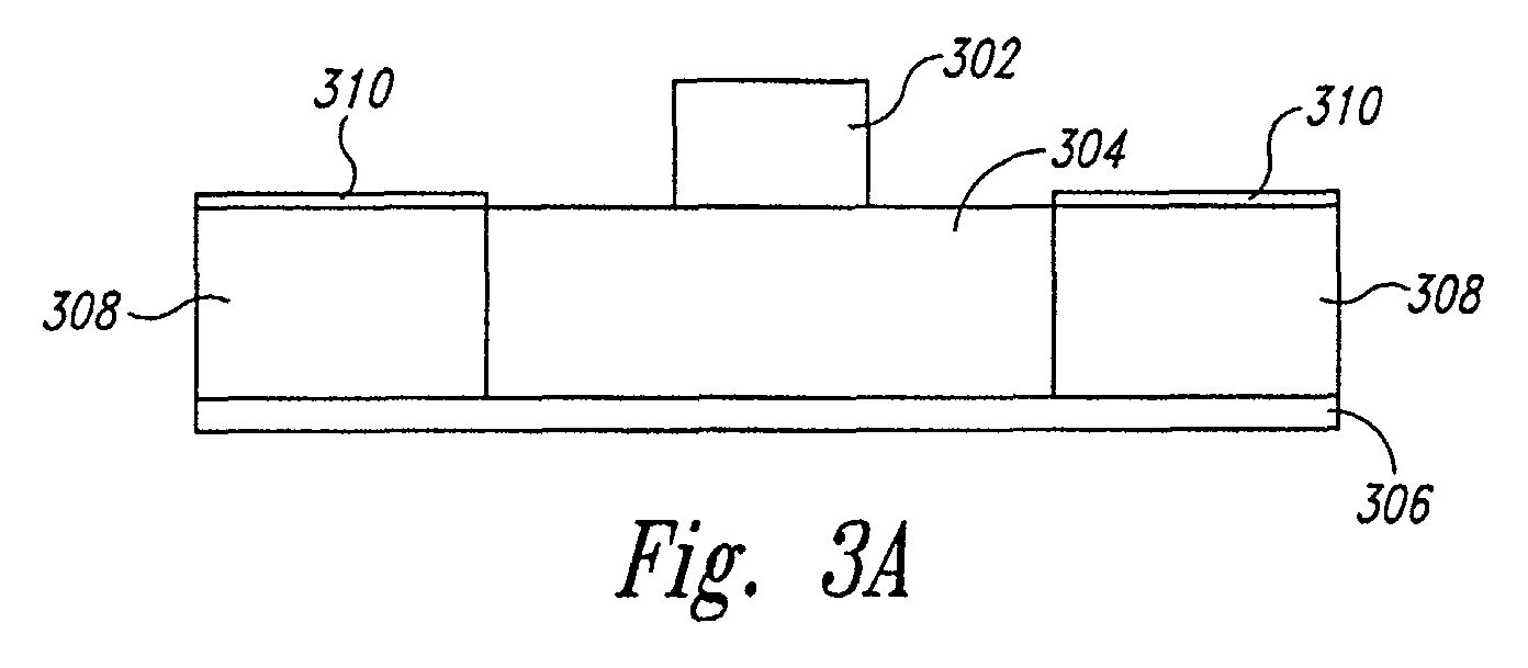
- FIGS. 3A-3D illustrate fabrication of a sharp silicon-based field emitter tip according to one embodiment of the present invention.
- Figure 3A illustrates a CMOS substrate that includes a deep polycrystalline or amorphous silicon well masked by a photoresist layer that represents the starting point for fabrication of a silicon-based field emitter tip.
- the photoresist layer 302 is created on top of the silicon well 304 by well-known photolithographic techniques.
- the silicon well 304 is itself layered on top of a metallic layer 306 that represents the cathode layer for the silicon-based field emitter tip to be fabricated.
- the silicon well 304 is surrounded on all sides by a dielectric layer 308.
- a second metal layer 3 10 serves, in the completed silicon-based field emitter device, as the electronic extraction anode.
- a plasma etch media may be used that employs one of the follow gases or gas mixtures: Cl 2 , BCl 3 , SiCl 4 /Cl 2 , BCl 3 /Cl 2 , HBr/Cl 2 /O 2 , HBr/O 2 , Br 2 /SF 6 , SF 6 , CF 4 , CF 3 Br, or HBr/NF 3 .
- Figure 3B shows the rough silicon-based field emitter tip following fluorine-based plasma etching of the silicon well. Note that a block of photoresist 302 remains above the rough field emitter tip 3 12.
- the photoresist mask is stripped off by well-known photoresist stripping methods, such as plasma O 2 stripping or various types of wet stripping using solvent strippers, sulfonic acid and chlorinated hydrocarbon solvent strippers, or chromic sulfuric acid mixtures.
- Figure 3C shows the rough silicon-based field emitter tip following photoresist stripping. Note that the rough silicon-based field emitter tip 3 12 has a blunt, or mesa-like point 3 14 following photoresist stripping.
- xenon difluoride, XeF 2 , isotropic silicon etching is employed to sharpen the rough silicon-based field emitter tip illustrated in Figure 3C.
- Figure 3D illustrates the sharpened silicon-based field emitter tip following XeF 2 etching.
- XeF 2 etching is carried out by sublimating XeF 2 crystals and introducing the resulting XeF 2 gas into a process chamber.
- XeF2 etching occurs at room temperature without the need for creating a plasma.
- XeF 2 etching provides extremely conformal isotropic etch profiles and reacts with silicon with high specificity. The reaction of the xenon difluoride with silicon produces volatile and easily removed silicon fluoride compounds.
- XeF 2 gas can be obtained by other well-known methods.
- Silicon-based field emitter tips can be micro-manufactured by microchip fabrication techniques as regular arrays, or grids, of field emitter tips. Uses for arrays of field emitter tips include computer display devices.
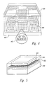
- Figure 4 illustrates a computer display device based on field emitter tip arrays. Arrays of silicon-based field emitter tips 402 are embedded into emitters 404 arrayed on the surface of a cathode base plate 406 and are controlled, by selective application of voltage, to emit electrons which are accelerated towards a face plate anode 408 coated with chemical phosphors. When the emitted electrons impact onto the phosphor, light is produced.
- the individual silicon-based field emitter tips have tip radii on the order of hundreds of Angstroms and emit currents of approximately 10 nanoamperes per tip under applied electrical field strengths of around 50 Volts.
- the method of the present invention may be used to prepare arrays of sharpened field emitter tips for use in such display devices.
- FIG. 5 illustrates an ultra-high density electromechanical memory based on a phase-change storage medium.
- the ultra-high density electromechanical memory comprises an air-tight enclosure 502 in which a silicon-based field emitter tip array 504 is mounted, with the field emitter tips vertically oriented in Figure 5, perpendicular to lower surface (obscured in Figure 5) of the silicon-based field emitter tip array 504.
- a phase-change storage medium 506 is positioned below the field emitter tip array, movably mounted to a micromover 508 which is electronically controlled by externally generated signals to precisely position the phase-change storage medium 506 with respect to the field emitter tip array 504.
- Small, regularly spaced regions of the surface of the phase-change storage medium 506 represent binary bits of memory, with each of two different solid states, or phases, of the phase-change storage medium 506 representing each of two different binary values.
- a relatively intense electron beam emitted from a field emitter tip can be used to briefly heat the area of the surface of the phase-change storage medium 506 corresponding to a bit to melt the phase-change storage medium underlying the surface.
- the melted phase-change storage medium may be allowed to cool relatively slowly, by relatively gradually decreasing the intensity of the electron beam to form a crystalline phase, or may be quickly cooled, quenching the melted phase-change storage medium to produce an amorphous phase.
- the phase of a region of the surface of the phase-change storage medium can be electronically sensed by directing a relatively low intensity electron beam from the field emitter tip onto the region and measuring secondary electron emission or electron backscattering from the region, the degree of secondary electron emission or electron backscattering dependent on the phase of the phase-change storage medium within the region.
- a partial vacuum is maintained within the airtight enclosure 502 so that gas molecules do not interfere with emitted electron beams.
- Dense fields of tiny field emitter tips microfabricated according to the present invention are particularly suitable for application in these ultra high-density electronic data storage devices.
- the method of the present invention may be used to prepare arrays of sharpened field emitter tips for use in such display devices.
- silicon-based field emitter tip sharpening may be employed for the final step of silicon-based field emitter tip sharpening.
- the silicon well from which the silicon-based field emitter tip is replicated may have various shapes and sizes created by well-known microchip fabrication techniques, depending on the final shape and size of the silicon-based field emitter tip desired. It may be possible to use layers other than photoresist layers to mask a portion of the' silicon well prior to the first isotropic etching step.
- the silicon well may be positioned on top of various different types of metallic and semiconductor substrates, or may be the surface portion of a silicon substrate, and the dielectric and metallic layers may have a variety of different compositions.
Landscapes
- Engineering & Computer Science (AREA)
- Manufacturing & Machinery (AREA)
- Cold Cathode And The Manufacture (AREA)
- Cathode-Ray Tubes And Fluorescent Screens For Display (AREA)
Abstract
Description
- The present invention relates to silicon-based field emitter tips and, in particular, to a method for sharpening silicon-based field emitter tips at low temperatures.
- The present invention relates to design and manufacture of field emitter tips, including silicon-based field emitter tips. A brief discussion of field emission and the principles of design and operation of field emitter tips is therefore first provided in the following paragraphs, with reference to Figures1 .
- When a wire, filament, or rod of a metallic or semiconductor material is heated, electrons of the material may gain sufficient thermal energy to escape from the material into a vacuum surrounding the material. The electrons acquire sufficient thermal energy to overcome a potential energy barrier that physically constrains the electrons to quantum states localized within the material. The potential energy barrier that constrains electrons to a material can be significantly reduced by applying an electric field to the material. When the applied electric field is relatively strong, electrons may escape from the material by quantum mechanical tunneling through a lowered potential energy barrier. The greater the magnitude of the electrical field applied to the wire, filament, or rod, the greater the current density of emitted electrons perpendicular to the wire, filament, or rod. The magnitude of the electrical field is inversely related to the radius of curvature of the wire, filament, or rod.
- Figure 1 illustrates principles of design and operation of a silicon-based field emitter tip. The
field emitter tip 102 rises to a verysharp point 104 from a silicon-substrate cathode 106, or electron source. A localized electric field is applied in the vicinity of the tip by afirst anode 108, or electron sink, having a disk-shaped aperture 110 above and around thepoint 104 of thefield emitter tip 102. Asecond cathode layer 112 is located above thefirst anode 108, also with a disk-shaped aperture 114 aligned directly above the disk-shaped aperture 110 of thefirst anode layer 108. Thissecond cathode layer 112 acts as a lens, applying a repulsive electronic field to focus the emitted electrons into a narrow beam. The emitted electrons are accelerated towards atarget anode 118, impacting in asmall region 120 of the target anode defined by the direction and width of the emittedelectron beam 116. Although Figure 1 illustrates a single field emitter tip, silicon-based field emitter tips are commonly micro-manufactured by microchip fabrication techniques as regular arrays, or grids, of field emitter tips. - Silicon-based field emitter tips are commonly located on the surface of complementary metal-oxide semiconductor ("CMOS") wafers. As discussed above, the current density of emitted electrons from a field emitter tips greatly increases with a decrease in the radius of the tip. Therefore, since it is desirable to achieve high current densities from silicon-based field emitter tips, tip sharpening procedures are normally employed in the final stage or stages of silicon-based field emitter tip array manufacture. Figures 2A-C illustrate a currently-available tip-sharpening procedure. In Figure 2A, a blunt silicon-based
field emitter tip 202 rises from aflat silicon substrate 204. In order to sharpen the tip, a thin surface layer of the field emitter tip and silicon substrate is heated to thermally oxidize silicon to SiO2. Figure 2B shows the field emitter tip shown in Figure 2A following thermal oxidation. The thin SIO2 layer 206 is grown inward from the surface of the field emitter tip and silicon substrate to produce a sharp, silicon-basedfield emitter tip 208 embedded within the thin SiO2 coating 206. Finally, the thin SIO2 layer is removed by hydrofluoric acid, HF, wet etching. Figure 2C shows the final sharp field emitter tip following HF wet etching. The point 2 10 of the final sharp field emitter tip may have a breadth of between 10 and several hundred Angstroms. - Thermal-oxide-based tip sharpening is effective and is commonly employed in current silicon-based field emitter tip application methodologies. However, especially when used to sharpen silicon-based field emitter tips fabricated on the surface of CMOS wafers, the thermal oxidation tip sharpening process has clear deficiencies due to the relatively high temperatures, commonly greater than 900 C, necessary to grow the surface layer of SiO2. A first deficiency is that the underlying CMOS circuitry may employ low-melting-point conductors that can be degraded by high temperature exposure. Thus, extremely precise application of heat must be carried out to grow the surface layer of SIO2 while not adversely effecting underlying CMOS circuitry. Often, to increase physical stability of silicon-based field emitter tips, a thin, metallic layer is deposited on the silicon surface of the field emitter tip. A second deficiency of thermal-oxide-based tip sharpening is that, once the metal is deposited, high-temperature sharpening processes can no longer be employed without melting or vaporizing the deposited metal. For these reasons, designers and manufacturers of silicon-based field emitter tips have recognized the need for an economical, low-temperature process for sharpening silicon-based field emitter tips.
- One embodiment of the present invention provides an efficient and economical process for sharpening silicon-based field emitter tips at low temperatures. A rough field emitter tip is carved out from a silicon well below a photoresist mask by isotropic plasma etching. The photoresist mask is removed, and the rough silicon-based field emitter tip that results is sharpened by isotropic xenon difluoride, XeF2 etching.
-
- Figure 1 illustrates principles of design and operation of a silicon-based field emitter tip.
- Figures 2A-C illustrate a currently available tip-sharpening procedure.
- Figures 3A-D illustrate fabrication of a sharp silicon-based field emitter tip according to one embodiment of the present invention.
- Figure 4 illustrates a computer display device based on field emitter tip arrays.
- Figure 5 illustrates an ultra-high density electromechanical memory based on a phase-change storage medium.
-
- One embodiment of the present invention provides a low-temperature method, compatible with CMOS substrates, for sharpening silicon-based field emitter tips. Figures 3A-3D illustrate fabrication of a sharp silicon-based field emitter tip according to one embodiment of the present invention. Figure 3A illustrates a CMOS substrate that includes a deep polycrystalline or amorphous silicon well masked by a photoresist layer that represents the starting point for fabrication of a silicon-based field emitter tip. The
photoresist layer 302 is created on top of thesilicon well 304 by well-known photolithographic techniques. Thesilicon well 304 is itself layered on top of ametallic layer 306 that represents the cathode layer for the silicon-based field emitter tip to be fabricated. Thesilicon well 304 is surrounded on all sides by adielectric layer 308. A second metal layer 3 10 serves, in the completed silicon-based field emitter device, as the electronic extraction anode. - In a first step for creating a silicon-based field emitter tip according to the present invention, one of many well-known isotropic plasma etching techniques is employed to isotropically etch the
silicon well 304 to produce a rough silicon-based field emitter tip below thephotoresist mask 302. For example, a plasma etch media may be used that employs one of the follow gases or gas mixtures: Cl2, BCl3, SiCl4/Cl2, BCl3/Cl2, HBr/Cl2/O2, HBr/O2, Br2/SF6, SF6, CF4, CF3Br, or HBr/NF3. Figure 3B shows the rough silicon-based field emitter tip following fluorine-based plasma etching of the silicon well. Note that a block ofphotoresist 302 remains above the rough field emitter tip 3 12. - In a second step, the photoresist mask is stripped off by well-known photoresist stripping methods, such as plasma O2 stripping or various types of wet stripping using solvent strippers, sulfonic acid and chlorinated hydrocarbon solvent strippers, or chromic sulfuric acid mixtures. Figure 3C shows the rough silicon-based field emitter tip following photoresist stripping. Note that the rough silicon-based field emitter tip 3 12 has a blunt, or mesa-like point 3 14 following photoresist stripping.
- Finally, xenon difluoride, XeF2, isotropic silicon etching is employed to sharpen the rough silicon-based field emitter tip illustrated in Figure 3C. Figure 3D illustrates the sharpened silicon-based field emitter tip following XeF2 etching. In one embodiment, XeF2 etching is carried out by sublimating XeF2 crystals and introducing the resulting XeF2 gas into a process chamber. XeF2 etching occurs at room temperature without the need for creating a plasma. XeF2 etching provides extremely conformal isotropic etch profiles and reacts with silicon with high specificity. The reaction of the xenon difluoride with silicon produces volatile and easily removed silicon fluoride compounds. In alternative embodiments, XeF2 gas can be obtained by other well-known methods.
- Silicon-based field emitter tips can be micro-manufactured by microchip fabrication techniques as regular arrays, or grids, of field emitter tips. Uses for arrays of field emitter tips include computer display devices. Figure 4 illustrates a computer display device based on field emitter tip arrays. Arrays of silicon-based field emitter
tips 402 are embedded intoemitters 404 arrayed on the surface of acathode base plate 406 and are controlled, by selective application of voltage, to emit electrons which are accelerated towards aface plate anode 408 coated with chemical phosphors. When the emitted electrons impact onto the phosphor, light is produced. In such applications, the individual silicon-based field emitter tips have tip radii on the order of hundreds of Angstroms and emit currents of approximately 10 nanoamperes per tip under applied electrical field strengths of around 50 Volts. The method of the present invention may be used to prepare arrays of sharpened field emitter tips for use in such display devices. - Silicon-based field emitter tips are also employed in various types of ultra-high density electronic data storage devices. Figure 5 illustrates an ultra-high density electromechanical memory based on a phase-change storage medium. The ultra-high density electromechanical memory comprises an air-
tight enclosure 502 in which a silicon-based fieldemitter tip array 504 is mounted, with the field emitter tips vertically oriented in Figure 5, perpendicular to lower surface (obscured in Figure 5) of the silicon-based fieldemitter tip array 504. A phase-change storage medium 506 is positioned below the field emitter tip array, movably mounted to amicromover 508 which is electronically controlled by externally generated signals to precisely position the phase-change storage medium 506 with respect to the fieldemitter tip array 504. Small, regularly spaced regions of the surface of the phase-change storage medium 506 represent binary bits of memory, with each of two different solid states, or phases, of the phase-change storage medium 506 representing each of two different binary values. A relatively intense electron beam emitted from a field emitter tip can be used to briefly heat the area of the surface of the phase-change storage medium 506 corresponding to a bit to melt the phase-change storage medium underlying the surface. The melted phase-change storage medium may be allowed to cool relatively slowly, by relatively gradually decreasing the intensity of the electron beam to form a crystalline phase, or may be quickly cooled, quenching the melted phase-change storage medium to produce an amorphous phase. The phase of a region of the surface of the phase-change storage medium can be electronically sensed by directing a relatively low intensity electron beam from the field emitter tip onto the region and measuring secondary electron emission or electron backscattering from the region, the degree of secondary electron emission or electron backscattering dependent on the phase of the phase-change storage medium within the region. A partial vacuum is maintained within theairtight enclosure 502 so that gas molecules do not interfere with emitted electron beams. Dense fields of tiny field emitter tips microfabricated according to the present invention are particularly suitable for application in these ultra high-density electronic data storage devices. The method of the present invention may be used to prepare arrays of sharpened field emitter tips for use in such display devices. - Although the present invention has been described in terms of a particular embodiment, it is not intended that the invention be limited to this embodiment. Modifications within the spirit of the invention will be apparent to those skilled in the art. For example, other low-temperature silicon etching gases, besides XeF2, that produce conformal isotropic etch profiles may be employed for the final step of silicon-based field emitter tip sharpening. The silicon well from which the silicon-based field emitter tip is replicated may have various shapes and sizes created by well-known microchip fabrication techniques, depending on the final shape and size of the silicon-based field emitter tip desired. It may be possible to use layers other than photoresist layers to mask a portion of the' silicon well prior to the first isotropic etching step. The silicon well may be positioned on top of various different types of metallic and semiconductor substrates, or may be the surface portion of a silicon substrate, and the dielectric and metallic layers may have a variety of different compositions.
- The foregoing description, for purposes of explanation, used specific nomenclature to provide a thorough understanding of the invention. However, it will be apparent to one skilled in the art that the specific details are not required in order to practice the invention. The foregoing descriptions of specific embodiments of the present invention are presented for purpose of illustration and description. They are not intended to be exhaustive or to limit the invention to the precise forms disclosed. Obviously many modifications and variations are possible in view of the above teachings. The embodiments are shown and described in order to best explain the principles of the invention and its practical applications, to thereby enable others skilled in the art to best utilize the invention and various embodiments with various modifications as are suited to the particular use contemplated. It is intended that the scope of the invention be defined by the following claims and their equivalents:
Claims (10)
- A method for sharpening a silicon-based field emitter tip, the method comprising:enclosing the silicon-based field emitter tip within a process chamber;producing a room-temperature gas that reacts with silicon with high specificity and that produces a conformal isotropic etch profile; andintroducing the room-temperature gas into the process chamber to isotropically etch the rough field emitter tip (312) to sharpness.
- The method of claim 1 wherein the room-temperature gas is xenon difluoride.
- A method for fabricating a sharp, silicon-based field emitter tip, the method comprising:microfabricating a silicon well (304), surrounded laterally by a dielectric layer (308), above an underlying first metal layer (306) with a second metal layer (310) overlying the dielectric layer leaving a surface area of the silicon well exposed;isotropically etching silicon within the silicon well (304) to create a rough field emitter tip (312) above the first metal layer; andisotropically etching the rough field emitter tip (312) with a room-temperature gas to produce the final, sharp silicon-based field emitter tip.
- The method of claim 3 wherein isotropically etching silicon within the silicon well (304) to create a rough field emitter tip (312) above the first metal layer (306) further comprises:applying a photoresist layer to surface of the second metal layer;photolithographically patterning a photoresist mask (302) on the exposed surface of the silicon well (304), roughly centered within the exposed surface of the silicon well, with a surface area less than the surface area of the silicon well;isotropically etching silicon within the silicon well to create a rough field emitter tip (312) above the first metal layer (306) and below the photoresist mask (302); andremoving the photoresist mask (302) following isotropically etching silicon within the silicon well (304).
- The method of claim 3 wherein isotropically etching silicon within the silicon well (304) to create a rough field emitter tip (312) above the first metal layer (306) and below the photoresist mask (302) further includes exposing the photoresist-masked silicon well to a plasma etch medium.
- The method of claim 3 wherein the plasma etch medium employs a gas or gas mixture selected from various gas or gas mixtures that include:Cl2;BCl3;SiCl4/Cl2;BCl3/Cl2;HBr/Cl2/O2;HBr/O2;Br2/SF6;SF6;CF4;CF3Br;and HBr/NF3.
- The method of claim 3 wherein the photoresist mask (302) is removed following isotropically etching silicon within the silicon well (304) by a removal method selected from among removal methods that include:plasma O2 stripping; andexposing the photoresist mask to a stripping solution selected from among stripping solutions includinga solvent-based stripping solution,a sulfonic acid and chlorinated hydrocarbon solvent stripping solution, anda chromic acid and sulfuric acid stripping solution.
- The method of claim 3 applied to array of silicon-based field emitter tips to produce an array of sharp, silicon-based field emitter tips.
- The method of claim 3 wherein the room-temperature gas is xenon difluoride.
- A method for preparing an array of sharp, silicon-based field emitter tips for use as a component in an electronic device, the method comprising:microfabricating an array of silicon wells (304), each well surrounded laterally by a dielectric layer (308), above an underlying first metal layer (306) with a second metal layer (310) overlying the dielectric layer (308) leaving a surface area of the silicon well exposed;isotropically etching silicon within the silicon wells (304) to create an array of rough field emitter tips (312) above the first metal layer (306);isotropically etching the rough field emitter tips (312) with a room-temperature gas to produce an array of sharp, silicon-based field emitter tips; andincluding the array of sharp, silicon-based field emitter tips in the electronic device.
Applications Claiming Priority (2)
| Application Number | Priority Date | Filing Date | Title |
|---|---|---|---|
| US880160 | 2001-06-12 | ||
| US09/880,160 US6648710B2 (en) | 2001-06-12 | 2001-06-12 | Method for low-temperature sharpening of silicon-based field emitter tips |
Publications (1)
| Publication Number | Publication Date |
|---|---|
| EP1267381A1 true EP1267381A1 (en) | 2002-12-18 |
Family
ID=25375630
Family Applications (1)
| Application Number | Title | Priority Date | Filing Date |
|---|---|---|---|
| EP02253772A Withdrawn EP1267381A1 (en) | 2001-06-12 | 2002-05-29 | Method for low temeperature sharpening of silicon based field emitter tips |
Country Status (3)
| Country | Link |
|---|---|
| US (1) | US6648710B2 (en) |
| EP (1) | EP1267381A1 (en) |
| JP (1) | JP2003007202A (en) |
Families Citing this family (3)
| Publication number | Priority date | Publication date | Assignee | Title |
|---|---|---|---|---|
| TW530423B (en) * | 2001-12-31 | 2003-05-01 | Nanya Technology Corp | Manufacturing method of emitter tips |
| US20070243714A1 (en) * | 2006-04-18 | 2007-10-18 | Applied Materials, Inc. | Method of controlling silicon-containing polymer build up during etching by using a periodic cleaning step |
| US9711392B2 (en) | 2012-07-25 | 2017-07-18 | Infineon Technologies Ag | Field emission devices and methods of making thereof |
Citations (4)
| Publication number | Priority date | Publication date | Assignee | Title |
|---|---|---|---|---|
| EP0379298A2 (en) * | 1989-01-18 | 1990-07-25 | THE GENERAL ELECTRIC COMPANY, p.l.c. | Method of forming an electrode for an electron emitting device |
| EP0731490A2 (en) * | 1995-03-02 | 1996-09-11 | Ebara Corporation | Ultra-fine microfabrication method using an energy beam |
| WO1999062106A2 (en) * | 1998-05-22 | 1999-12-02 | The University Of Birmingham | Method of producing a structured surface |
| US6057172A (en) * | 1997-09-26 | 2000-05-02 | Nec Corporation | Field-emission cathode and method of producing the same |
Family Cites Families (13)
| Publication number | Priority date | Publication date | Assignee | Title |
|---|---|---|---|---|
| NL160425C (en) * | 1971-08-17 | 1979-10-15 | Philips Nv | METHOD OF MANUFACTURING AN ELECTRICAL DISCHARGE TUBE, INCLUDING AN ELECTRON-EMITTING ELECTRODE, CONSISTING OF A SUPPORT, ONTO WHICH A CAESIUM-CONTAINING LAYER HAS BEEN APPLIED, AND ELECTRICAL DISCHARGE TUBE. |
| US5090932A (en) | 1988-03-25 | 1992-02-25 | Thomson-Csf | Method for the fabrication of field emission type sources, and application thereof to the making of arrays of emitters |
| KR970007786B1 (en) * | 1993-11-08 | 1997-05-16 | 이종덕 | Preparation process of silicon field emitter array |
| US5557596A (en) | 1995-03-20 | 1996-09-17 | Gibson; Gary | Ultra-high density storage device |
| JP3171785B2 (en) | 1996-06-20 | 2001-06-04 | 富士通株式会社 | Thin display device and method of manufacturing field emission cathode used therefor |
| US5857885A (en) * | 1996-11-04 | 1999-01-12 | Laou; Philips | Methods of forming field emission devices with self-aligned gate structure |
| KR100279737B1 (en) * | 1997-12-19 | 2001-02-01 | 정선종 | Short-wavelength photoelectric device composed of field emission device and optical device and fabrication method thereof |
| US6010918A (en) * | 1998-02-10 | 2000-01-04 | Fed Corporation | Gate electrode structure for field emission devices and method of making |
| JPH11306957A (en) * | 1998-04-15 | 1999-11-05 | Yamaha Corp | Manufacture of electric field emission element |
| US6137212A (en) | 1998-05-26 | 2000-10-24 | The United States Of America As Represented By The Secretary Of The Army | Field emission flat panel display with improved spacer architecture |
| JP2000011859A (en) | 1998-06-22 | 2000-01-14 | Yamaha Corp | Manufacture of field emission type element |
| US6417016B1 (en) * | 1999-02-26 | 2002-07-09 | Micron Technology, Inc. | Structure and method for field emitter tips |
| US6448100B1 (en) * | 2001-06-12 | 2002-09-10 | Hewlett-Packard Compnay | Method for fabricating self-aligned field emitter tips |
-
2001
- 2001-06-12 US US09/880,160 patent/US6648710B2/en not_active Expired - Lifetime
-
2002
- 2002-05-29 EP EP02253772A patent/EP1267381A1/en not_active Withdrawn
- 2002-06-10 JP JP2002168908A patent/JP2003007202A/en active Pending
Patent Citations (4)
| Publication number | Priority date | Publication date | Assignee | Title |
|---|---|---|---|---|
| EP0379298A2 (en) * | 1989-01-18 | 1990-07-25 | THE GENERAL ELECTRIC COMPANY, p.l.c. | Method of forming an electrode for an electron emitting device |
| EP0731490A2 (en) * | 1995-03-02 | 1996-09-11 | Ebara Corporation | Ultra-fine microfabrication method using an energy beam |
| US6057172A (en) * | 1997-09-26 | 2000-05-02 | Nec Corporation | Field-emission cathode and method of producing the same |
| WO1999062106A2 (en) * | 1998-05-22 | 1999-12-02 | The University Of Birmingham | Method of producing a structured surface |
Non-Patent Citations (2)
| Title |
|---|
| HUQ S E ET AL: "FABRICATION OF SUB-10 NM SILICON TIPS: A NEW APPROACH", JOURNAL OF VACUUM SCIENCE AND TECHNOLOGY: PART B, AMERICAN INSTITUTE OF PHYSICS. NEW YORK, US, VOL. 13, NR. 6, PAGE(S) 2718-2721, ISSN: 0734-211X, XP000558344 * |
| MOREAU D ET AL: "PROCEDES DE FABRICATION DE MICROPOINTES EN SILICIUM", LE VIDE: SCIENCE, TECHNIQUE ET APPLICATIONS, SFV, FR, VOL. 52, NR. 282, PAGE(S) 463-477, ISSN: 1266-0167, XP000637302 * |
Also Published As
| Publication number | Publication date |
|---|---|
| JP2003007202A (en) | 2003-01-10 |
| US20020187714A1 (en) | 2002-12-12 |
| US6648710B2 (en) | 2003-11-18 |
Similar Documents
| Publication | Publication Date | Title |
|---|---|---|
| US5302238A (en) | Plasma dry etch to produce atomically sharp asperities useful as cold cathodes | |
| JP2612153B2 (en) | Method for forming a uniform array having a sharp tip | |
| US4307507A (en) | Method of manufacturing a field-emission cathode structure | |
| US9058954B2 (en) | Carbon nanotube field emission devices and methods of making same | |
| EP1018131B1 (en) | Gated electron emission device and method of fabrication thereof | |
| US5302239A (en) | Method of making atomically sharp tips useful in scanning probe microscopes | |
| US5757344A (en) | Cold cathode emitter element | |
| WO1997047020A9 (en) | Gated electron emission device and method of fabrication thereof | |
| US6448100B1 (en) | Method for fabricating self-aligned field emitter tips | |
| US20040046491A1 (en) | Enhanced electron field emitter spindt tip and method for fabricating enhanced spindt tips | |
| US6607415B2 (en) | Method for fabricating tiny field emitter tips | |
| US8159119B2 (en) | Vacuum channel transistor and manufacturing method thereof | |
| US5857885A (en) | Methods of forming field emission devices with self-aligned gate structure | |
| KR100250458B1 (en) | Method of manufacturing cathode tips of field emission devices | |
| US6648710B2 (en) | Method for low-temperature sharpening of silicon-based field emitter tips | |
| US7259510B1 (en) | On-chip vacuum tube device and process for making device | |
| US20050255613A1 (en) | Manufacturing of field emission display device using carbon nanotubes | |
| US6572425B2 (en) | Methods for forming microtips in a field emission device | |
| Lee et al. | Fabrication and characterization of silicon field emitter arrays with focusing electrode by the chemical mechanical polishing process | |
| WO1996000975A1 (en) | Fabrication of electron-emitting structures using charged-particle tracks and removal of emitter material | |
| Dziuban et al. | Mold-type field-emission array fabrication by the use of fast silicon etching | |
| JPH08129952A (en) | Manufacture of field emission type electron gun | |
| KR100218672B1 (en) | A structure and a fabrication method of vacuum element | |
| JP3649313B2 (en) | Method for producing carbon-based material-coated cold cathode and cold cathode | |
| KR100701750B1 (en) | Emitter Structure of Field Emission Device and Manufacturing Method Thereof |
Legal Events
| Date | Code | Title | Description |
|---|---|---|---|
| PUAI | Public reference made under article 153(3) epc to a published international application that has entered the european phase |
Free format text: ORIGINAL CODE: 0009012 |
|
| AK | Designated contracting states |
Kind code of ref document: A1 Designated state(s): AT BE CH CY DE DK ES FI FR GB GR IE IT LI LU MC NL PT SE TR |
|
| AX | Request for extension of the european patent |
Free format text: AL;LT;LV;MK;RO;SI |
|
| 17P | Request for examination filed |
Effective date: 20030320 |
|
| AKX | Designation fees paid |
Designated state(s): DE FR GB NL |
|
| RTI1 | Title (correction) |
Free format text: METHOD FOR LOW TEMPERATURE SHARPENING OF SILICON BASED FIELD EMITTER TIPS |
|
| GRAP | Despatch of communication of intention to grant a patent |
Free format text: ORIGINAL CODE: EPIDOSNIGR1 |
|
| STAA | Information on the status of an ep patent application or granted ep patent |
Free format text: STATUS: THE APPLICATION IS DEEMED TO BE WITHDRAWN |
|
| 18D | Application deemed to be withdrawn |
Effective date: 20061201 |